 | –≠–ª–µ–∫—Ç—Ä–æ–Ω–Ω—ã–π –∫–æ–º–ø–æ–Ω–µ–Ω—Ç: iC-OC | –°–∫–∞—á–∞—Ç—å:  PDF PDF  ZIP ZIP |

iC-OC
INTEGRATING LIGHT-VOLTAGE CONVERTER
Rev C2, Page 1/8
D1
D2
FEATURES
APPLICATIONS
À
Two photosensors with integrating amplifiers
À
Integration time can be set externally
À
Internal shift register for chain connection
À
Detection of low supply voltage
À
TTL/CMOS-compatible logic inputs and outputs
À
5V supply voltage
À
Low power consumption
À
Photosensors with 1mm pitch; active area
ca. 0.97mm x 0.47mm (0.44mm
2
)
À
Optical row sensors
À
As substitutes for CCDs
PACKAGES
1.7mm x 1.2mm
BLOCK DIAGRAM
© 2001
iC-Haus GmbH
Tel +49-6135-9292-0
Integrated Circuits
Fax +49-6135-9292-192
Am Kuemmerling 18, D-55294 Bodenheim
http://www.ichaus.com
R
Q1
C
C
R
R
Q4
Q3
C
R
Q2
C
AOUT
CLK
DIN
DOUT
GND
VDD
+5V
1k
R1
SHIFT REGISTER
LOW VOLTAGE
INTEGRATOR 1
VDD - 1.2V
SC1
iC-OC
INTEGRATOR 2
SC2
VDD - 1.2V
SOUT1
SOUT2
ANALOG OUTPUT
INPUT
BUFFER
D1
D2
D
D
D
D
VOUT

iC-OC
INTEGRATING LIGHT-VOLTAGE CONVERTER
Rev C2, Page 2/8
DESCRIPTION
iC-OC is an optical sensor with two photodiodes, two integrating amplifiers and a control logic which enables
several iC-OCs to be connected in a chain.
Furthermore, the control logic, consisting of a two-stage shift register, determines when the integration time
starts and ends and switches the integrators in sequence to the analog output. The analog output is a source
follower and in its deactivated state has a high impedance and can thus be used in buses.
The control logic output supplies a CMOS-compatible signal and in chain connection it can be directly linked
to the digital input of the next device. Logic inputs are configured as Schmitt triggers and are TTL/CMOS-
compatible.
All the registers in the device are reset with low voltage (power-down reset).
All pins are protected against ESD.
CHIP LAYOUT
PAD DESCRIPTION
(top view)
Name
Function
DIN
Input
CLK
Clock Input
DOUT
Data Output
VDD
+5V Supply Voltage
AOUT
Analog Output
GND
Ground
iC-OC
INTEGRATING LIGHT-VOLTAGE CONVERTER
Rev C2, Page 3/8
All voltages are referenced to ground unless otherwise noted.
All currents into the device pins are positive; all currents out of the device pins are negative.
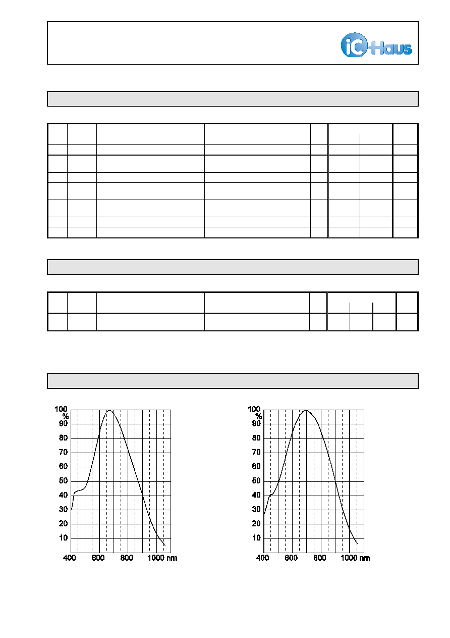
Relative Spectral Sensitivity
Relative Spectral Sensitivity with BMST assembly
ABSOLUTE MAXIMUM RATINGS
Values beyond which damage may occur; device operation is not guaranteed.
Item Symbol
Parameter
Conditions
Fig.
Unit
Min.
Max.
G001 VDD
Supply Voltage
-0.3
6.5
V
G002 Ic()
Clamping Current in DIN, CLK, DOUT,
AOUT
-20
20
mA
G003 I()
Current in DOUT
-10
10
mA
G004 Ilu()
Pulse Current in all Pins
(Latch-up strength)
pulse width
# 10µs
-100
100
mA
E001 Vd()
ESD Susceptibility, at all Pins
MIL-STD-883, Method 3015, HBM
100pF discharged through 1.5k
2
kV
TG1 Tj
Junction Temperature
-40
150
∞C
TG2 Ts
Storage Temperature
see package specification
THERMAL DATA
Operating Conditions: VDD= 5V ±10%
Item Symbol
Parameter
Conditions
Fig.
Unit
Min.
Typ.
Max.
T1
Ta
Operating Ambient Temperature
Range
see package specification
ELECTRICAL CHARACTERISTICS: Diagrams

iC-OC
INTEGRATING LIGHT-VOLTAGE CONVERTER
Rev C2, Page 4/8
ELECTRICAL CHARACTERISTICS
Operating Conditions:
VDD= 5V ±10%, RL(VDD/AOUT)= 1k, Tj= 0..85
EC unless otherwise noted
Item
Symbol
Parameter
Conditions
Tj
Fig.
Unit
∞C
Min.
Typ.
Max.
Total Device
001 VDD
Permissible Supply Voltage
Range
4.5
5.5
V
002 I(VDD)
Supply Current in VDD
100
700
µA
003 Vc()hi
Clamp Voltage hi at
DIN, CLK, DOUT, AOUT
Vc()hi= V() -VDD, I()= 10mA
other pins open
0.3
1.5
V
004 Vc()lo
Clamp Voltage lo at
DIN, CLK, DOUT, AOUT
I()= -10mA, other pins open
-1.5
-0.3
V
005 Aph()
Radiant Sensitive Area
ca. 0.97 x 0.47
mm
2
006 ar
Spectral Application Range
S(ar)= 0.25 x S()max
300
950
nm
Analog Output AOUT
201 V0()
Output Voltage at no Illuminance V0()= VDD -V(AOUT)max,
AOUT active (* see below)
0.8
1.4
V
202 vd()
Variation of Output Voltage at no
Illuminance
Vd()= V(AOUT)t1 -V(AOUT)t2,
t= t2 -t1= 1ms
-10
10
mV
203 Vs()
Saturation Voltage
tenfold illuminance
VDD= 4.5V
VDD= 5V
VDD= 5.5V
1.4
1.45
1.5
V
V
V
204 V()
Repeatability
(Standard deviation at repeated
measurement)
20 measurements at constant
LED Illuminance, Vav(AOUT)
.
2.91V, t= 25µs
15
mV
205 Vlin()
Output Voltage Linearity Range
Vlin()= VDD -V0() -V(AOUT)
1.7
V
206 K
Transfer Factor Output Voltage
vs. Light Power
BMST assembly incl. sealing;
LED
= 628nm, = ±23nm
LED
= 880nm, = ±40nm
0.22
0.13
0.27
0.16
0.32
0.19
V/
pWs
207 klin
Transfer Factor Deviation within
Linearity Range
-5
5
%
208 I()
Leakage Current
V(AOUT)= 0..VDD, AOUT high
impedance (* see below)
-2
2
µA
Shift-Register Inputs DIN, CLK
301 Vt()hi
Threshold Voltage hi at DIN, CLK
2.2
V
302 Vt()lo
Threshold Voltage lo at DIN, CLK
0.8
V
303 Vt()hys
Hysteresis at DIN, CLK
Vt()hys= Vt()hi -Vt()lo
250
1300
mV
304 Ii()
Input Current in DIN, CLK
V()= 0..VDD
-1
1
µA
305 f()
Permissible Frequency at CLK
10
MHz
306 tw()hi
Permis. Pulse Width hi at CLK
20
ns
307 tw()lo
Permis. Pulse Width lo at CLK
20
ns
308 tplh
Propagation Delay:
CLK hi
6lo until DOUT lo6hi
CL(DOUT)= 50pF
2
40
ns
309 tphl
Propagation Delay:
CLK hi
6lo until DOUT hi6lo
CL(DOUT)= 50pF
2
40
ns
310 tpon
Propagation Delay:
CLK lo
6hi until AOUT active
CL(VDD/AOUT)= 1nF
2
800
ns
311 tpoff
Propagation Delay: CLK lo
6hi
until AOUT high impedance
CL(VDD/AOUT)= 1nF
2
100
ns

iC-OC
INTEGRATING LIGHT-VOLTAGE CONVERTER
Rev C2, Page 5/8
ELECTRICAL CHARACTERISTICS
Operating Conditions:
VDD= 5V ±10%, RL(VDD/AOUT)= 1k, Tj= 0..85
EC unless otherwise noted
Item
Symbol
Parameter
Conditions
Tj
Fig.
Unit
∞C
Min.
Typ.
Max.
Buffer DOUT
312 Vs()hi
Saturation Voltage hi
Vs()hi= VDD -V(), I()= -1mA
0.4
V
314 Vs()lo
Saturation Voltage lo
I()= 1mA
0.4
V
Low Voltage Detection
401 VDDon
Turn-on Threshold VDD
increasing voltage at VDD
2.3
3.8
V
402 VDDoff
Undervoltage Threshold VDD
decreasing voltage at VDD
1.0
2.1
V
403 VDDhys Hysteresis VDDhys=
VDDon
-VDDoff
0.5
2
V
(*) AOUT active: SOUT1 or SOUT2 closed; AOUT high impedance: SOUT1 and SOUT2 open.