 | –≠–ª–µ–∫—Ç—Ä–æ–Ω–Ω—ã–π –∫–æ–º–ø–æ–Ω–µ–Ω—Ç: iC-WGBLCC | –°–∫–∞—á–∞—Ç—å:  PDF PDF  ZIP ZIP |
iC-WG
14-BIT DIFFERENTIAL SCANNING OPTO ENCODER
FEATURES
APPLICATIONS
Excellent matching and reliability due to monolithic
construction with integrated photodiodes
Short track pitch (600
µ
m)
Elimination of dark currents due to differential scanning
Photocurrent amplifier with high cut-off frequency
Current comparators with acurately tracked hysteresis
Current-limited push-pull outputs
Adjustable LED current control for constant receive power
Integrated power driver for the transmit LED
LED current monitor with error message output
Integrated test aid1
Low power consumption
Broad operating voltage range, from 4.5V to 20V
Available as 28-pin BLCC or as chip
Options: extended temperature range of -30..110
∞
C,
customized packages, reticle assembly, code disc
Optical position decoding with
14-bit resolution based on the
principle of differential scanning
CHIP
2.97mm
◊
8.71mm
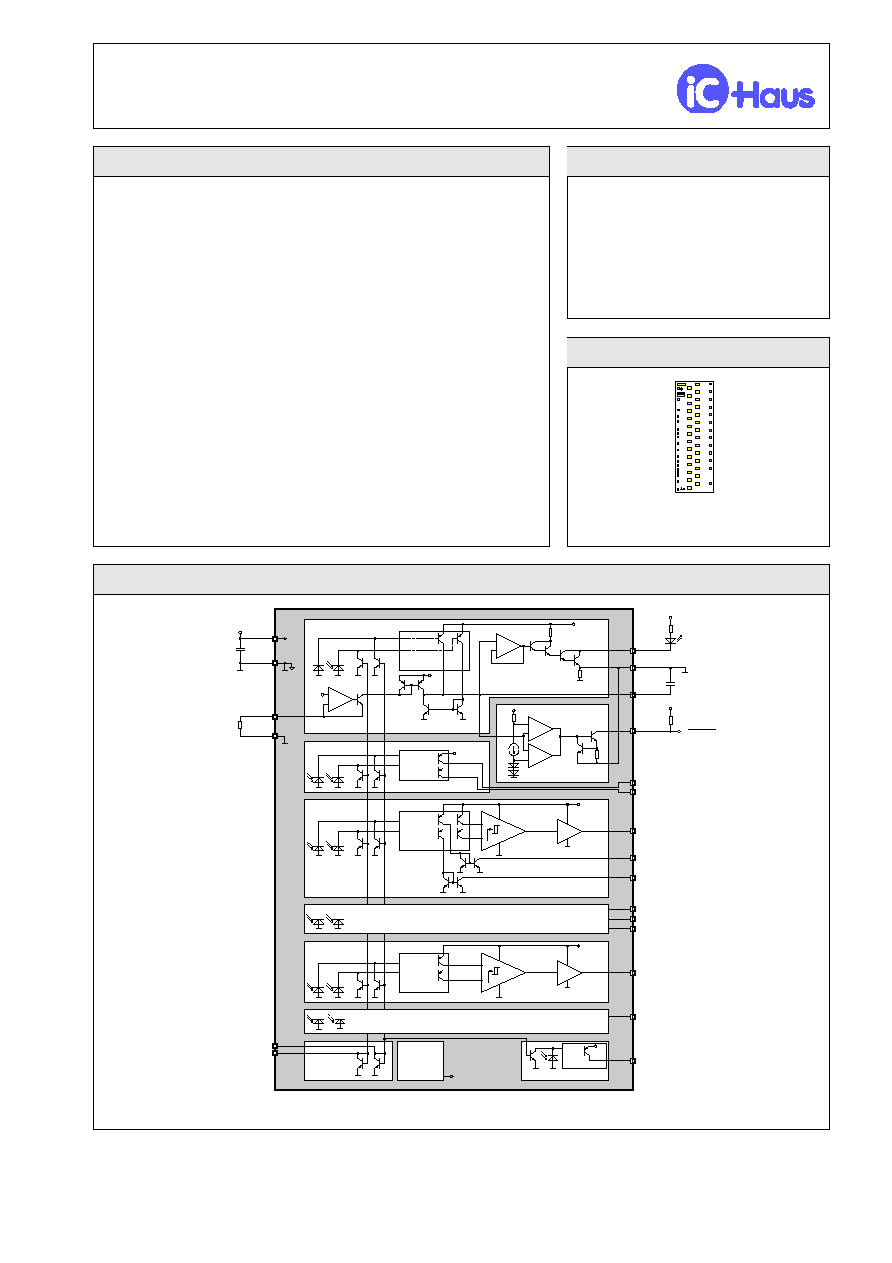
BLOCK DIAGRAM
©1999
Rev B0
COMPARATOR
PUSH-PULL
TEST
TRACK 2
TRACK 3..13
TRACK 1
TRACK 0
AMPLIFIER
BIAS
LED-CURRENT CONTROL
AMPLIFIER
(see TRACK 0)
(see TRACK 2)
AMPLIFIER
TRACK POSITION
AMPLIFIER
CONTROL
MONITOR
COMPARATOR
PUSH-PULL
AMPLIFIER
DSR (REF.)
N
P
P
N
N
P
P
N
P
N
MONITOR
..13
A2
IN1
IP1
A1
RGND
TIP
TIN
VCC
GND
VCC
A0
LED
IP0
IN0
LGND
CSR
RSR
1.2V
1.2V
VCC
VCC
VCC
VCC
IM1
VCC
VCC
VCC
NERR
A3
IMP
IMN
R2
50
100nF
C2
LED
R1
50k
-
+
+
-
-
+
-
+
4.5..20V
C1
100nF
5..25V
ERROR
R3
10k
iC-WG
OUTPUT
OUTPUT
14
1
7
6
12
13
8
9
11
10
n.c.
n.c.
28
3
27
5
4
26
25..15
n.c.
2
BLCC WGC2
DR
iC-Haus GmbH
Tel
+49-6135-9292-0
Integrated Circuits
Fax +49-6135-9292-192
Am Kuemmerling 18, D-55294 Bodenheim
http://www.ichaus.com

iC-WG
14-BIT DIFFERENTIAL SCANNING OPTO ENCODER
Rev B0, Page 2/11
DESCRIPTION
The iC-WG is an optoelectronic detector IC for linear and angle measuring systems, e.g. glass scales or
rotary encoders. Monolithically integrated are photodiodes, amplifiers and comparators as well as
TTL-compatible push-pull output drivers. All 14 tracks are differentially evaluated.
An integrated LED current control with driver stage makes it possible to directly connect a transmit LED
with series resistor and also guarantees a constant optical received power. The setpoint for the receive
current is adjusted via an external resistor. If the LED current control deviates from its working range, this
is indicated at the error message output.
For the adjustment of a reticle the chip features two adjustment crosses and supplies the analog signals
from three monitor photocurrent amplifiers. For exact radial alignment of the iC-WG (with reticle) to the
code disk, two monitor photodiodes are arranged such that the track position can be checked (option, not
available in the standard SMD package).
Two test pins permit a complete electrical functional test of the IC not including the photodiodes.
All push-pull and analog outputs are protected against ESD and short-circuits. The error message output
NERR is also short-circuit-proof and due to it's open-collector design bus capable.
PAD DESCRIPTION
Name
Function
GND
Ground
IN0
Track N0 Analog Output (current sink)
IP0
Track P0 Analog Output (current sink)
IN1
Track N1 Analog Output (current sink)
IP1
Track P1 Analog Output (current sink)
RGND
Reference Ground for RSR circuitry
RSR
LED Current Control Setup
LED
LED Driver Output
LGND
LED Driver Power Ground
NERR
Error Message Output, low active
CSR
External capacitor for LED control
TIP
Positive Test Aid Input
TIN
Negative Test Aid Input
VCC
+5 to +20V Supply Voltage
A13
Track 13 Push-Pull Output
A12
"
..
"
A0
Track 0 Push-Pull Output
iC-WG
14-BIT DIFFERENTIAL SCANNING OPTO ENCODER
Rev B0, Page 3/11
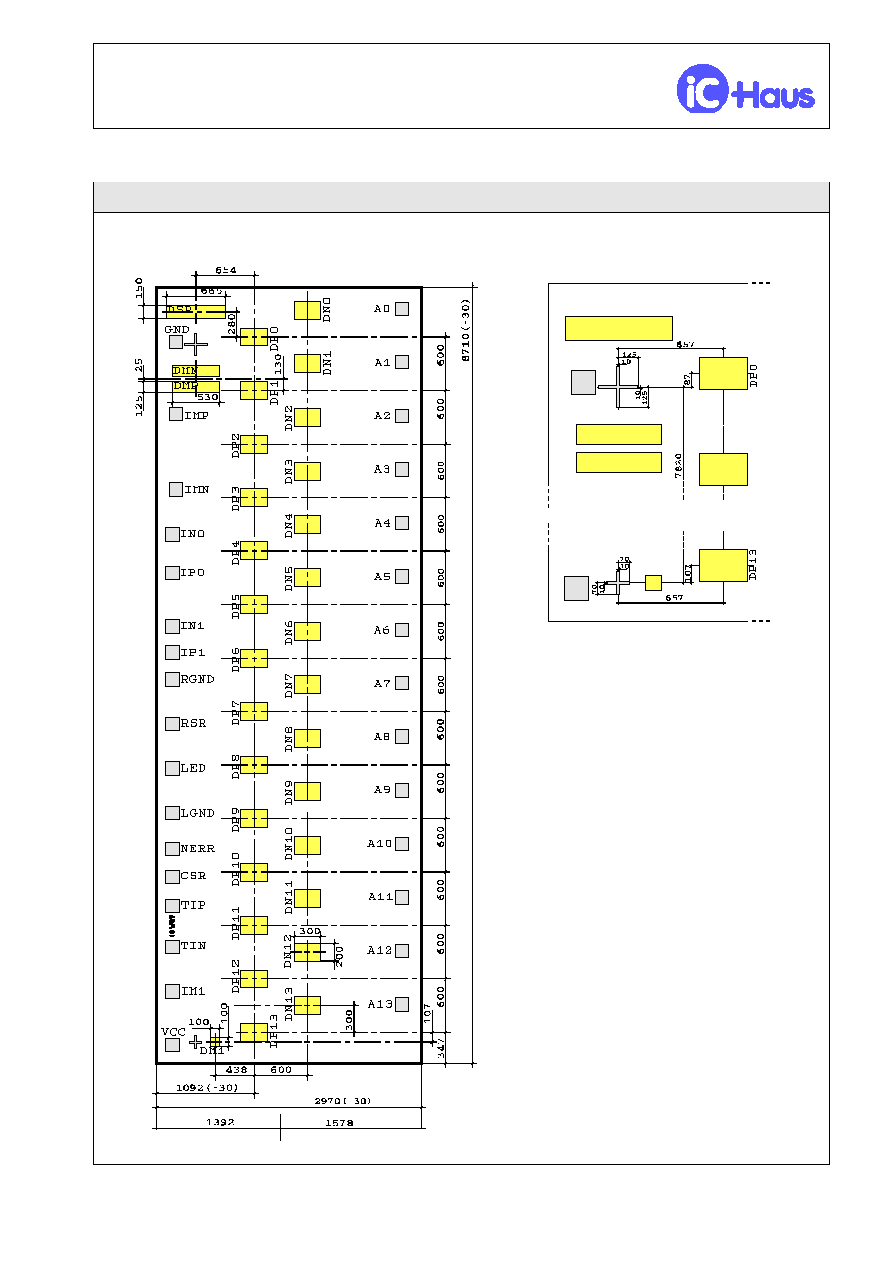
CHIP LAYOUT
dimensions in
µ
m; chip size 2.97mm
◊
8.71mm
iC-WG
14-BIT DIFFERENTIAL SCANNING OPTO ENCODER
Rev B0, Page 4/11
ABSOLUTE MAXIMUM RATINGS
Values beyond which damage may occur; device operation is not guaranteed.
Item
Symbol
Parameter
Conditions
Fig.
Unit
Min.
Max.
G001 VCC
Supply Voltage
0
21
V
G301 V(A)
Voltage at Outputs A0..13
0
VCC
G302 I(A)
Current in Outputs A0..13
V(A)< 0V or V(A)> VCC
-3
3
mA
G501 I(IM1)
Current in Monitor Output IM1
-1
1
mA
G601 I(TIP)
I(TIN)
Current in TIP, TIN
-1
1
mA
G701 I(RSR)
Current in RSR
-1
0.1
mA
G702 I(RGND)
Current in RGND
-5
5
mA
G703 I(LED)
Current in LED
V(LED)> VCC
0
3
mA
G704 I(LED
-LGND)
Current in LED to LGND
0
150
mA
G705 I(LGND)
Current in LGND
LED and NERR open
-3
3
mA
G706 V(CSR)
Voltage at CSR
0
VCC
G707 I(CSR)
Current in CSR
-1
1
mA
G802 I(IPi)
I(INi)
Current in Analog Outputs
IP0, IN0, IP1, IN1
-1
3
mA
G902 I(IMP)
I(IMN)
Current in Monitor Outputs
IMP, IMN
-1
1
mA
GA01 V(NERR) Voltage at NERR
LGND at GND
0
30
V
E001 Vd()
ESD Susceptibility at all Pins
MIL-STD 883, Method 3015, HBM,
100pF discharged through 1.5k
2
kV
TG1 Tj
Junction Temperature
-30
125
∞
C
TG2 Ts
Storage Temperature
see package specification
THERMAL DATA
Operating Conditions: VCC= 4.5..20V
Item
Symbol
Parameter
Conditions
Fig.
Unit
Min.
Typ.
Max.
T1
Ta
Operating Ambient Temperature
Range
see package specification
All voltages are referenced to ground unless otherwise noted.
All currents into the device pins are positive; all currents out of the device pins are negative.

iC-WG
14-BIT DIFFERENTIAL SCANNING OPTO ENCODER
Rev B0, Page 5/11
ELECTRICAL CHARACTERISTICS
Operating Conditions: VCC= 4.5..20V, Tj= -20..125
∞
C, unless otherwise noted
Item
Symbol
Parameter
Conditions
Tj
Fig.
Unit
∞
C
Min.
Typ.
Max.
Total Device
001
VCC
Permissible Supply Voltage
4.5
20
V
002
I(VCC)
Supply Current in VCC,
Outputs A0..13 hi
LED control active:
R(RSR/RGND)= 140k
, NERR=hi
I(LED)
8mA, I(A0..13)= 0;
I(DP0..13)=30nA, I(DN0..13)=3nA,
VCC= 5V
-20
27
85
125
3.0
5.4
5.9
6.2
6.2
10.7
mA
mA
mA
mA
mA
see above, VCC= 20V
-20
27
85
125
3.3
6.4
6.7
7.0
7.4
14.6
mA
mA
mA
mA
mA
003
I(VCC)
Supply Current in VCC,
Outputs A0..13 lo
LED control active:
R(RSR/RGND)= 14k
, NERR=hi
I(LED)
80mA, I(A0..13)= 0;
I(DP0..13)=3nA, I(DN0..13)=30nA,
VCC= 5V
-20
27
85
125
6.0
11.7
12.8
13.6
13.8
25.5
mA
mA
mA
mA
mA
see above, VCC= 20V
-20
27
85
125
6.8
14.6
16.3
17.0
17.4
38.5
mA
mA
mA
mA
mA
004
fo
Cut-off Frequency,
tracks 0..13
sinusoidal waveform,
I(DP0..13)= 3..30nA
I(DN0..13)= 30..3nA
100
kHz
005
tp(D-A)
Switch Delay
see No. 004
2.5
µ
s
006
fo
Cut-off Frequency,
tracks 0..13
sinusoidal waveform,
I(DP0..13)= 6..60nA
I(DN0..13)= 60..6nA
200
kHz
007
tp(D-A)
Switch Delay
see No. 006
1.5
µ
s
Photodiodes DP0..13, DN0..13, DSR, DMP, DMN, DM1
008
S(
)max
Spectral Sensitivity
= 850nm
0.5
A/W
009
ar
Range of Spectral Sensitivity
Se(
ar)= 0.1
◊
S(
)max
500
1050
nm
Photodiodes and Amplifiers with Analog Outputs, track 0 and 1
801
Aph(D)
Radiant Sensitive Area
0.2
◊
0.3
mm≤
802
I(D)
Permissible Photocurrent
90
nA
803
Ierr
Error Current at Photodiodes
-20
27
85
125
4.7
3.6
3.2
15.5
20
15
15
25
nA
nA
nA
nA
804
CM()
Common Mode DPi to DNi
0.85
1
1.15
805
CR()
Current Gain
I(IPi) / I(DPi),
I(INi) / I(DNi)
V(IPi,INi)= 1V..VCC,
I(DPi,DNi)= 3..90nA
600
900
806
CR()
Current Gain
I(IPi) / I(DPi),
I(INi) / I(DNi)
VCC= 5V, V(IPi,INi)= 2V,
I(DPi,DNi)= 30nA
27
740
807
TC(CR)
Temperature Coefficient of
Current Gain CR
Tj< 90
∞
C
-0.03
%/K
808
I0(IPi)
I0(INi)
Analog Output Leakage Current
V(IPi,INi)= 1V..VCC,
I(DPi,DNi)= 0
10
µ
A