
IC71V08F32xS08
IC71V16F32xS08
2
Integrated Circuit Solution Inc.
MCP001-0A 7/04/2002
MCP FEATURES
� Power supply voltage 2.7V to 3.3V
� High performance:
Flash: 85ns maximum access time
SRAM: 70ns maximum access time
� Package:
64-ball BGA - 32 Mbit Flash/8 Mbit SRAM
� Operating Temperature: -25
o
C to +85
o
C
FLASH FEATURES
� Two bank organization enabling simultaneous execution
of erase/ program and read
� Bank organization: 2 banks (16 Mbits + 16 Mbits)
� Memory organization: 4,194,304 words x 8 bits (BYTE
mode)
2,097,152 words x 16 bits (WORD
mode)
� Sector organization: 71 sectors (8 Kbytes/ 4 Kwords x 8
sectors, 64 Kbytes/ 32 Kwords x 63 sectors)
� Bottom boot sector organization
- Boot sector allocated to the lowest address (sector)
� 3-state output
� Automatic program
- Program suspend/ resume
� Unlock bypass program
� Automatic erase
- Chip erase
- Sector erase (sectors can be combined freely)
- Erase suspend/ resume
� Program/ Erase completion detection
- Detection through data polling and toggle bits
- Detection through RY/
BY
pin
� Sector group protection
- Any sector group can be protected
- Any protected sector group can be temporary unpro-
tected
� Sectors can be used for boot application
� Hardware reset and standby using
RESET
pin
� Automatic sleep mode
� Boot block sector protect by
WP
(ACC) pin
� Conforms to common flash memory interface (CFI)
� Extra One Time Protect Sector provided
3.0 Volt-Only Flash & SRAM COMBO with Stacked Multi-Chip
Package (MCP) - 32 Mbit Simultaneous Operation Flash
Memory and 8 Mbit Static RAM
ICSI reserves the right to make changes to its products at any time without notice in order to improve design and supply the best possible product. We assume no responsibility for any errors
which may appear in this publication. � Copyright 2000, Integrated Circuit Solution Inc.
� Access time: 85ns (MAX.)
� Operating supply voltage: 2.7 to 3.3V
� Power supply current (Active mode)
- Read: 16mA (MAX.)
- Program/ Erase: 30mA (MAX.)
� Standby current: 5 �A (MAX.)
� Operating ambient temperature: -25 to +85
o
C
� Program/ erase time
- Program 9.0 �s/ byte (TYP.)
11.0 �s/ word (TYP.)
- Sector erase: 0.7s (TYP.)
� Number of program/ erase: 1,000,000 times (MIN)
SRAM FEATURES (8 Mb density)
� Power Dissipation:
Operating: 25 mA maximum
Standby: 15 �A maximum
� Chip Selects:
CE1
s, CE2s
� Power down feature using
CE1
s , or CE2s or
LB
s &
UB
s
� Data retention supply voltage: 1.2 to 3.3 volt
� Byte data control:
LB
s (DQ-VDQ7),
UB
s (DQ8-DQ15) -
on x16 version
GENERAL DESCRIPTION
The flash and SRAM MCP is available in 32 Mbit Flash/8
Mbit SRAM having a data bus of either x8 or x16. The 32
Mbit flash is composed of 2,097,152 words of 16 bits or 4,
194,304 bytes of 8 bits. Data lines DQ0-DQ7 handle the x8
format, while lines DQ0-DQ15 handle the x16 format.
The package uses a 3.0V power supply for all operations. No
other source is required for program and erase operations. The
flash can be programmed in system using this 3.0V supply,
or can be programmed in a standard EPROM programmer.
The 32 Mbit flash/8 Mbit SRAM is offered in a 64-pin BGA
package. The flash is compatible with the JEDEC Flash
command set standard. The flash access time is 85ns and
the SRAM access time is 70ns.
The Flash architecture is composed of two banks which
allows simultaneous operation on each. Optimized perfor-
mance can be achieved by first initializing a program or
erase function in one bank, then immediately starting a read
from the other bank. Both operations would then be operat-
ing simultaneously, with zero latency.
IC71V08F32xS08
IC71V16F32xS08
Integrated Circuit Solution Inc.
5
MCP001-0A 7/04/2002
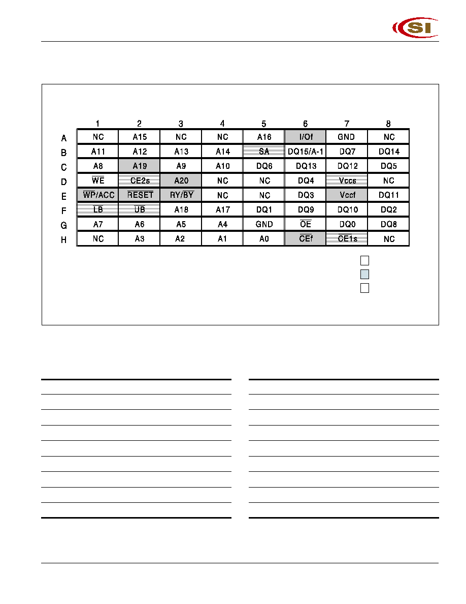
PIN CONFIGURATION (32 Mb Flash and 8 Mb SRAM)
64 BALL FBGA (Top View)
Shared
Flash only
SRAM only
PIN DESCRIPTIONS
A0-A18
Address Inputs, Common
A19-A20, A-1
Address Inputs, Flash
DQ0-DQ15/A-1 Data Inputs/Outputs
RESET
Reset
CE1
s, CE2s
Chip Selects, SRAM
I/Of
I/O Configuration, Flash
CE
f
Chip Enable Input, Flash
OE
Output Enable Input
WE
Write Enable Input
LB
s
Lower-byte Control(DQ0-DQ7), SRAM
UB
s
Upper-byte Control (DQ8-DQ15), SRAM
WP
/ACC
Write Protect/Acceleration Pin, Flash
RY/
BY
Ready/Busy Output
SA
High Order Address Pin, SRAM (x8)
NC
No Connection
Vccf
Power, Flash
V
CCS
Power, SRAM
GND
Ground


