ICSI reserves the right to make changes to its products at any time without notice in order to improve design and supply the best possible product. We assume no responsibility for any errors
which may appear in this publication. © Copyright 2000, Integrated Circuit Solution Inc.
FEATURES
·
Extended Data-Out (EDO) Page Mode access cycle
·
TTL compatible inputs and outputs; tristate I/O
·
Refresh Interval:
Refresh Mode: 1,024 cycles /16 ms
RAS-Only, CAS-before-RAS (CBR), and Hidden
Self refresh Mode - 1,024 cycles / 128ms
·
JEDEC standard pinout
·
Single power supply:
5V ± 10% (IS41C16100S)
3.3V ± 10% (IS41LV16100S)
·
Byte Write and Byte Read operation via two
CAS
·
Industrail Temperature Range -40°C to 85°C
DESCRIPTION
The
ICSI
IS41C16100S and IS41LV16100S are 1,048,576 x
16-bit high-performance CMOS Dynamic Random Access
Memories. These devices offer an accelerated cycle access
called EDO Page Mode. EDO Page Mode allows 1,024 ran-
dom accesses within a single row with access cycle time as
short as 20 ns per 16-bit word. The Byte Write control, of upper
and lower byte, makes the IS41C16100S ideal for use in
16-, 32-bit wide data bus systems.
These features make the IS41C16100Sand IS41LV16100S
ideally suited for high-bandwidth graphics, digital signal
processing, high-performance computing systems, and
peripheral applications.
The IS41C16100S and IS41LV16100S are packaged in a
42-pin 400mil SOJ and 400mil 50- (44-) pin TSOP-2.
IS41C16100S
IS41LV16100S
1M x 16 (16-MBIT) DYNAMIC RAM
WITH EDO PAGE MODE
EY TIMING PARAMETERS
Parameter
-45
(1)
-50
-60
Unit
Max.
RAS Access Time (t
RAC
)
45
50
60
ns
Max.
CAS Access Time (t
CAC
)
11
13
15
ns
Max. Column Address Access Time (t
AA
)
22
25
30
ns
Min. EDO Page Mode Cycle Time (t
PC
)
16
20
25
ns
Min. Read/Write Cycle Time (t
RC
)
77
84
104
ns
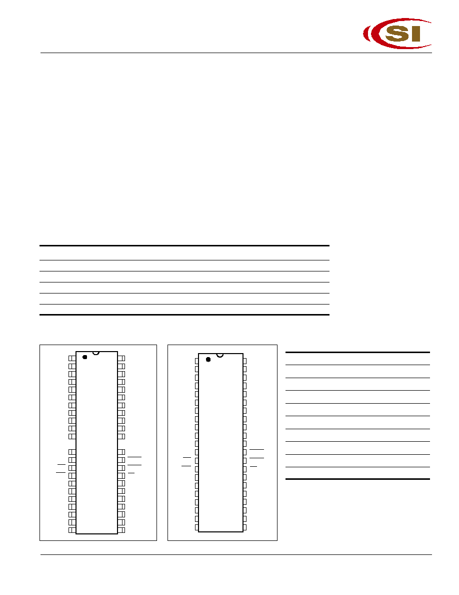
42-Pin SOJ
PIN CONFIGURATIONS
50(44)-Pin TSOP II
1
2
3
4
5
6
7
8
9
10
11
12
13
14
15
16
17
18
19
20
21
42
41
40
39
38
37
36
35
34
33
32
31
30
29
28
27
26
25
24
23
22
VCC
I/O0
I/O1
I/O2
I/O3
VCC
I/O4
I/O5
I/O6
I/O7
NC
NC
WE
RAS
NC
NC
A0
A1
A2
A3
VCC
GND
I/O15
I/O14
I/O13
I/O12
GND
I/O11
I/O10
I/O9
I/O8
NC
LCAS
UCAS
OE
A9
A8
A7
A6
A5
A4
GND
PIN DESCRIPTIONS
A0-A9
Address Inputs
I/O0-15
Data Inputs/Outputs
WE
Write Enable
OE
Output Enable
RAS
Row Address Strobe
UCAS
Upper Column Address Strobe
LCAS
Lower Column Address Strobe
Vcc
Power
GND
Ground
NC
No Connection
1
2
3
4
5
6
7
8
9
10
11
15
16
17
18
19
20
21
22
23
24
25
50
49
48
47
46
45
44
43
42
41
40
36
35
34
33
32
31
30
29
28
27
26
VCC
I/O0
I/O1
I/O2
I/O3
VCC
I/O4
I/O5
I/O6
I/O7
NC
NC
NC
WE
RAS
NC
NC
A0
A1
A2
A3
VCC
GND
I/O15
I/O14
I/O13
I/O12
GND
I/O11
I/O10
I/O9
I/O8
NC
NC
LCAS
UCAS
OE
A9
A8
A7
A6
A5
A4
GND
Integrated Circuit Solution Inc.
1
DR004-0B
Note:
1.
45 ns Only for Vcc = 3.3V.

IS41C16100S
IS41LV16100S
4
Integrated Circuit Solution Inc.
DR004-0B
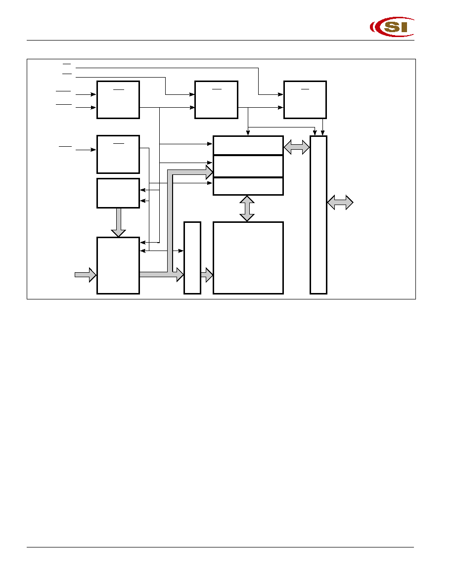
Functional Description
The IS41C16100S and IS41LV16100S is a CMOS DRAM
o p t i m i z e d f o r h i g h - s p e e d b a n d w i d t h , l o w p o w e r
applications. During READ or WRITE cycles, each bit is
uniquely addressed through the 16 address bits. These
are entered ten bits (A0-A9) at a time. The row address is
latched by the Row Address Strobe (
RAS). The column
address is latched by the Column Address Strobe (
CAS).
RAS is used to latch the first ten bits and CAS is used the
latter ten bits.
The IS41C16100S and IS41LV16100S has two
CAS
controls,
LCAS and UCAS. The LCAS and UCAS inputs
internally generates a
CAS signal functioning in an iden-
tical manner to the single
CAS input on the other 1M x 16
DRAMs. The key difference is that each
CAS controls its
corresponding I/O tristate logic (in conjunction with
OE
and
WE and RAS). LCAS controls I/O0 through I/O7 and
UCAS controls I/O8 through I/O15.
The IS41C16100S and IS41LV16100S
CAS function is
determined by the first
CAS (LCAS or UCAS) transitioning
LOW and the last transitioning back HIGH. The two
CAS
controls give the IS41C16100S and IS41LV16100S both
BYTE READ and BYTE WRITE cycle capabilities.
Memory Cycle
A memory cycle is initiated by bring
RAS LOW and it is
terminated by returning both
RAS and CAS HIGH. To
ensures proper device operation and data integrity any
memory cycle, once initiated, must not be ended or
aborted before the minimum t
RAS
time has expired. A new
cycle must not be initiated until the minimum precharge
time t
RP
, t
CP
has elapsed.
Read Cycle
A read cycle is initiated by the falling edge of
CAS or OE,
whichever occurs last, while holding
WE HIGH. The
column address must be held for a minimum time specified
by t
AR
. Data Out becomes valid only when t
RAC
, t
AA
, t
CAC
and t
OEA
are all satisfied. As a result, the access time is
dependent on the timing relationships between these
parameters.
Write Cycle
A write cycle is initiated by the falling edge of
CAS and
WE, whichever occurs last. The input data must be valid
at or before the falling edge of
CAS or WE, whichever
occurs first.
Refresh Cycle
To retain data, 1,024 refresh cycles are required in each
16 ms period. There are two ways to refresh the memory.
1. By clocking each of the 1,024 row addresses (A0
through A9) with
RAS at least once every 16 ms. Any
read, write, read-modify-write or
RAS-only cycle re-
freshes the addressed row.
2. Using a
CAS-before-RAS refresh cycle. CAS-before-
RAS refresh is activated by the falling edge of RAS,
while holding
CAS LOW. In CAS-before-RAS refresh
cycle, an internal 10-bit counter provides the row
addresses and the external address inputs are ignored.
CAS-before-RAS is a refresh-only mode and no data
access or device selection is allowed. Thus, the output
remains in the High-Z state during the cycle.
Self Refresh Cycle
The Self Refresh allows the user a dynamic refresh, data
retention mode at the extended refresh period of 128 ms.
i.e., 125 µs per row when using distributed CBR refreshes.
The feature also allows the user the choice of a fully static,
low power data retention mode. The optional Self Refresh
feature is initiated by performing a CBR Refresh cycle and
holding
RAS LOW for the specified t
RAS
.
The Self Refresh mode is terminated by driving
RAS HIGH
for a minimum time of t
RP
. This delay allows for the
completion of any internal refresh cycles that may be in
process at the time of the
RAS LOW-to-HIGH transition.
If the DRAM controller uses a distributed refresh sequence,
a burst refresh is not required upon exiting Self Refresh.
However, if the DRAM controller utilizes a
RAS-only or
burst refresh sequence, all 1,024 rows must be refreshed
within the average internal refresh rate, prior to the re-
sumption of normal operation.
Extended Data Out Page Mode
EDO page mode operation permits all 1,024 columns
within a selected row to be randomly accessed at a high
data rate.
In EDO page mode read cycle, the data-out is held to the
next
CAS cycle's falling edge, instead of the rising edge.
For this reason, the valid data output time in EDO page
mode is extended compared with the fast page mode. In
the fast page mode, the valid data output time becomes
shorter as the
CAS cycle time becomes shorter. Therefore,
in EDO page mode, the timing margin in read cycle is
larger than that of the fast page mode even if the
CAS
cycle time becomes shorter.
In EDO page mode, due to the extended data function, the
CAS cycle time can be shorter than in the fast page mode
if the timing margin is the same.
The EDO page mode allows both read and write opera-
tions during one
RAS cycle, but the performance is
equivalent to that of the fast page mode in that case.
Power-On
After application of the V
CC
supply, an initial pause of
200 µs is required followed by a minimum of eight initial-
ization cycles (any combination of cycles containing a
RAS signal).
During power-on, it is recommended that
RAS track with
V
CC
or be held at a valid V
IH
to avoid current surges.