ICSI reserves the right to make changes to its products at any time without notice in order to improve design and supply the best possible product. We assume no responsibility for any errors
which may appear in this publication. © Copyright 2000, Integrated Circuit Solution Inc.
.EATURES
Extended Data-Out (EDO) Page Mode access cycle
TTL compatible inputs and outputs; tristate I/O
Refresh Interval: 1024 cycles /16 ms
Refresh Mode: RAS-Only, CAS-before-RAS (CBR),
Hidden
JEDEC standard pinout
Single power supply:
5V ± 10% (IS41C8512)
3.3V ± 10% (IS41LV8512)
Byte Write and Byte Read operation via CAS
Industrail Temperature Range -40
o
C to 85
o
C
DESCRIPTION
The
1+51
IS41C8512 and IS41LV8512 is a 524,288 x 8-bit
high-performance CMOS Dynamic Random Access Memories.
The IS41C8512 offer an accelerated cycle access called EDO
Page Mode. EDO Page Mode allows 512 random accesses
within a single row with access cycle time as short as 10 ns per
8-bit.
These features make the IS41C8512and IS41LV8512 ideally
suited for high-bandwidth graphics, digital signal processing,
high-performance computing systems, and peripheral
applications.
The IS41C8512 is packaged in a 28-pin 400mil SOJ and
400mil TSOP-2.
IS41C8512
IS41LV8512
512K x 8 (4-MBIT) DYNAMIC RAM
WITH EDO PAGE MODE
KEY TIMING PARAMETERS
Parameter
-35
-50
-60
Unit
Max. RAS Access Time (t
RAC
)
35
50
60
ns
Max. CAS Access Time (t
CAC
)
10
14
15
ns
Max. Column Address Access Time (t
AA
)
18
25
30
ns
Min. EDO Page Mode Cycle Time (t
PC
)
12
20
25
ns
Min. Read/Write Cycle Time (t
RC
)
60
90
110
ns
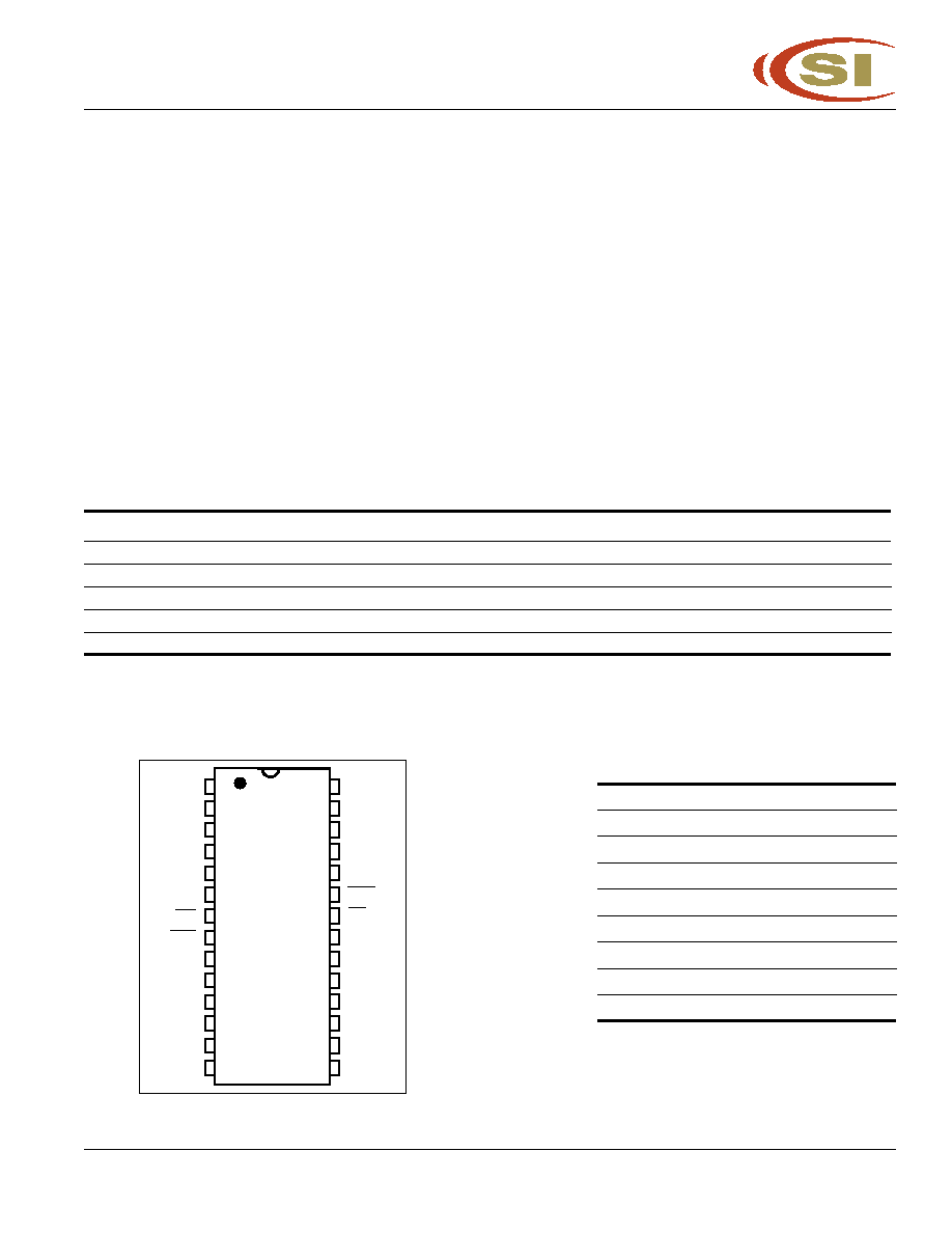
PIN CON.IGURATIONS
28 Pin SOJ, TSOP-2
PIN DESCRIPTIONS
A0-A9
Address Inputs
I/O0-7
Data Inputs/Outputs
WE
Write Enable
OE
Output Enable
RAS
Row Address Strobe
CAS
Column Address Strobe
Vcc
Power
GND
Ground
NC
No Connection
Integrated Circuit Solution Inc.
1
DR008-0B
1
2
3
4
5
6
7
8
9
10
11
12
13
14
28
27
26
25
24
23
22
21
20
19
18
17
16
15
VCC
I/O0
I/O1
I/O2
I/O3
NC
WE
RAS
A9
A0
A1
A2
A3
VCC
GND
I/O7
I/O6
I/O5
I/O4
CAS
OE
NC
A8
A7
A6
A5
A4
GND

IS41C8512
IS41LV8512
Integrated Circuit Solution Inc.
3
DR008-0B
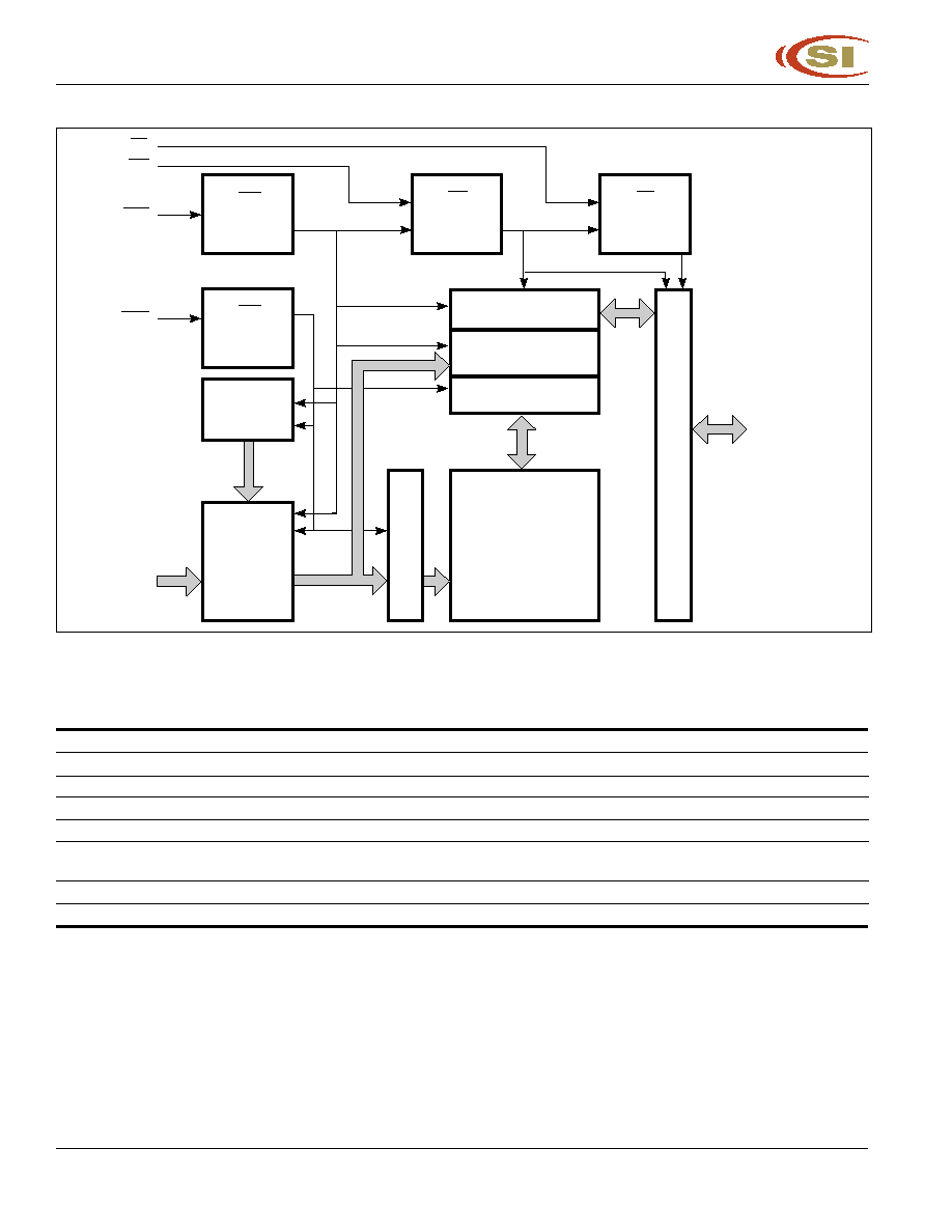
.unctional Description
The IS41C8512 and IS41LV8512 is a CMOS DRAM
optimized for high-speed bandwidth, low power
applications. During READ or WRITE cycles, each bit is
uniquely addressed through the 10 address bits. These
are entered ten bits (A0-A9) at a time. The row address is
latched by the Row Address Strobe (RAS). The column
address is latched by the Column Address Strobe (CAS).
RAS is used to latch the first ten bits and CAS is used the
latter nine bits.
Memory Cycle
A memory cycle is initiated by bring RAS LOW and it is
terminated by returning both RAS and CAS HIGH. To
ensures proper device operation and data integrity any
memory cycle, once initiated, must not be ended or
aborted before the minimum t
RAS
time has expired. A new
cycle must not be initiated until the minimum precharge
time t
RP
, t
CP
has elapsed.
Read Cycle
A read cycle is initiated by the falling edge of CAS or OE,
whichever occurs last, while holding WE HIGH. The
column address must be held for a minimum time specified
by t
AR
. Data Out becomes valid only when t
RAC
, t
AA
, t
CAC
and t
OEA
are all satisfied. As a result, the access time is
dependent on the timing relationships between these
parameters.
Write Cycle
A write cycle is initiated by the falling edge of CAS and
WE, whichever occurs last. The input data must be valid
at or before the falling edge of CAS or WE, whichever
occurs first.
Refresh Cycle
To retain data, 1024 refresh cycles are required in each
16 ms period. There are two ways to refresh the memory.
1. By clocking each of the 1024 row addresses (A0
through A9) with RAS at least once every 16 ms. Any
read, write, read-modify-write or RAS-only cycle re-
freshes the addressed row.
2. Using a CAS-before-RAS refresh cycle. CAS-before-
RAS refresh is activated by the falling edge of RAS,
while holding CAS LOW. In CAS-before-RAS refresh
cycle, an internal 10-bit counter provides the row ad-
dresses and the external address inputs are ignored.
CAS-before-RAS is a refresh-only mode and no data
access or device selection is allowed. Thus, the output
remains in the High-Z state during the cycle.
Extended Data Out Page Mode
EDO page mode operation permits all 512 columns within
a selected row to be randomly accessed at a high data
rate.
In EDO page mode read cycle, the data-out is held to the
next CAS cycles falling edge, instead of the rising edge.
.or this reason, the valid data output time in EDO page
mode is extended compared with the fast page mode. In
the fast page mode, the valid data output time becomes
shorter as the CAS cycle time becomes shorter. Therefore,
in EDO page mode, the timing margin in read cycle is
larger than that of the fast page mode even if the CAS cycle
time becomes shorter.
In EDO page mode, due to the extended data function, the
CAS cycle time can be shorter than in the fast page mode
if the timing margin is the same.
The EDO page mode allows both read and write opera-
tions during one RAS cycle, but the performance is equiva-
lent to that of the fast page mode in that case.
Power-On
After application of the V
CC
supply, an initial pause of
200 µs is required followed by a minimum of eight initial-
ization cycles (any combination of cycles containing a
RAS signal).
During power-on, it is recommended that RAS track with
V
CC
or be held at a valid V
IH
to avoid current surges.
IS41C8512
IS41LV8512
4
Integrated Circuit Solution Inc.
DR008-0B
ABSOLUTE MAXIMUM RATINGS
(1)
Symbol
Parameters
Rating
Unit
V
T
Voltage on Any Pin Relative to GND
5V
1.0 to +7.0
V
3.3V
0.5 to +4.6
V
CC
Supply Voltage
5V
1.0 to +7.0
V
3.3V
0.5 to +4.6
I
OUT
Output Current
50
mA
P
D
Power Dissipation
1
W
T
A
Commercial Operation Temperature
0 to +70
°C
Industrial Operationg Temperature
40 to +85
°C
T
STG
Storage Temperature
55 to +125
°C
Note:
1. Stress greater than those listed under ABSOLUTE MAXIMUM RATINGS may cause permanent
damage to the device. This is a stress rating only and functional operation of the device at these
or any other conditions above those indicated in the operational sections of this specification is
not implied. Exposure to absolute maximum rating conditions for extended periods may affect
reliability.
RECOMMENDED OPERATING CONDITIONS
(Voltages are referenced to GND.)
Symbol
Parameter
Min.
Typ.
Max.
Unit
V
CC
Supply Voltage
5V
4.5
5.0
5.5
V
3.3V
3.0
3.3
3.6
V
IH
Input High Voltage
5V
2.4
V
CC
+ 1.0
V
3.3V
2.0
V
CC
+ 0.3
V
IL
Input Low Voltage
5V
1.0
0.8
V
3.3V
0.3
0.8
T
A
Commercial Ambient Temperature
0
70
°C
Industrial Ambient Temperature
40
85
°C
CAPACITANCE
(1,2)
Symbol
Parameter
Max.
Unit
C
IN
1
Input Capacitance: A0-A8
5
p.
C
IN
2
Input Capacitance: RAS, UCAS, LCAS, WE, OE
7
p.
C
IO
Data Input/Output Capacitance: I/O0-I/O15
7
p.
Notes:
1. Tested initially and after any design or process changes that may affect these parameters.
2. Test conditions: T
A
= 25°C, f = 1 MHz.
IS41C8512
IS41LV8512
Integrated Circuit Solution Inc.
5
DR008-0B
ELECTRICAL CHARACTERISTICS
(1)
(Recommended Operating Conditions unless otherwise noted.)
Symbol Parameter
Test Condition
Speed Min.
Max.
Unit
I
IL
Input Leakage Current
Any input 0V < V
IN
< Vcc
10
10
µA
Other inputs not under test = 0V
I
IO
Output Leakage Current
Output is disabled (Hi-Z)
10
10
µA
0V < V
OUT
< Vcc
V
OH
Output High Voltage Level
I
OH
= 2.5 mA
2.4
V
V
OL
Output Low Voltage Level
I
OL
=+2.1mA
0.4
V
I
CC
1
Standby Current: TTL
RAS, CAS > V
IH
Commerical 5V
3
mA
Industrial
5V
4
Commerical 3V
2
Industrial
3V
3
I
CC
2
Standby Current: CMOS
RAS, CAS > V
CC
0.2V
5V
2
mA
3V
1
I
CC
3
Operating Current:
RAS, CAS,
-35
230
mA
Random Read/Write
(2,3,4)
Address Cycling, t
RC
= t
RC
(min.)
-50
180
Average Power Supply Current
-60
170
I
CC
4
Operating Current:
RAS = V
IL
, CAS,
-35
220
mA
EDO Page Mode
(2,3,4)
Cycling t
PC
= t
PC
(min.)
-50
170
Average Power Supply Current
-60
160
I
CC
5
Refresh Current:
RAS Cycling, CAS > V
IH
-35
230
mA
RAS-Only
(2,3)
t
RC
= t
RC
(min.)
-50
180
Average Power Supply Current
-60
170
I
CC
6
Refresh Current:
RAS, CAS Cycling
-35
230
mA
CBR
(2,3,5)
t
RC
= t
RC
(min.)
-50
180
Average Power Supply Current
-60
170
Notes:
1. An initial pause of 200 µs is required after power-up followed by eight RAS refresh cycles (RAS-Only or CBR) before proper device
operation is assured. The eight RAS cycles wake-up should be repeated any time the t
RE.
refresh requirement is exceeded.
2. Dependent on cycle rates.
3. Specified values are obtained with minimum cycle time and the output open.
4. Column-address is changed once each EDO page cycle.
5. Enables on-chip refresh and address counters.