 | –≠–ª–µ–∫—Ç—Ä–æ–Ω–Ω—ã–π –∫–æ–º–ø–æ–Ω–µ–Ω—Ç: 180M-01 | –°–∫–∞—á–∞—Ç—å:  PDF PDF  ZIP ZIP |

ICS180-01
Low EMI Clock Generator
MDS 180-01 B
1
Revision 050405
I n t e gra t e d C i r c u i t S y s t e m s
l
5 2 5 R a c e S t r e e t , S a n J o s e, C A 9 5 1 2 6
l
t e l ( 4 0 8 ) 2 9 7 - 1 2 0 1
l
w w w. i c s t . c o m
Description
The ICS180-01 generates a low EMI output clock from
a clock or crystal input. The device uses ICS'
proprietary mix of analog and digital Phase Locked
Loop (PLL) technology to spread the frequency
spectrum of the output, thereby reducing the frequency
amplitude peaks by several dB.
The ICS180-01 offers down spread selection of -1.25%
and -3.75%. Refer to the MK1714-01/02 for the widest
selection of input frequencies and multipliers.
ICS offers a complete line of EMI reducing clock
generators. Consult us when you need to remove
crystals and oscillators from your board.
Features
∑
Pin and function compatible to Cypress W180-01
∑
Packaged in 8-pin SOIC
∑
Provides a spread spectrum output clock
∑
Accepts a clock input and provides same frequency
dithered output
∑
Input frequency of 8 to 28 MHz
∑
Peak reduction by 7dB - 14dB typical on 3rd - 19th
odd harmonics
∑
Spread percentage selection for -1.25% and -3.75%
∑
Operating voltage of 3.3 V and 5 V
∑
Advanced, low-power CMOS process
∑
Available in Pb (lead) free package
∑
Industrial temperature range available
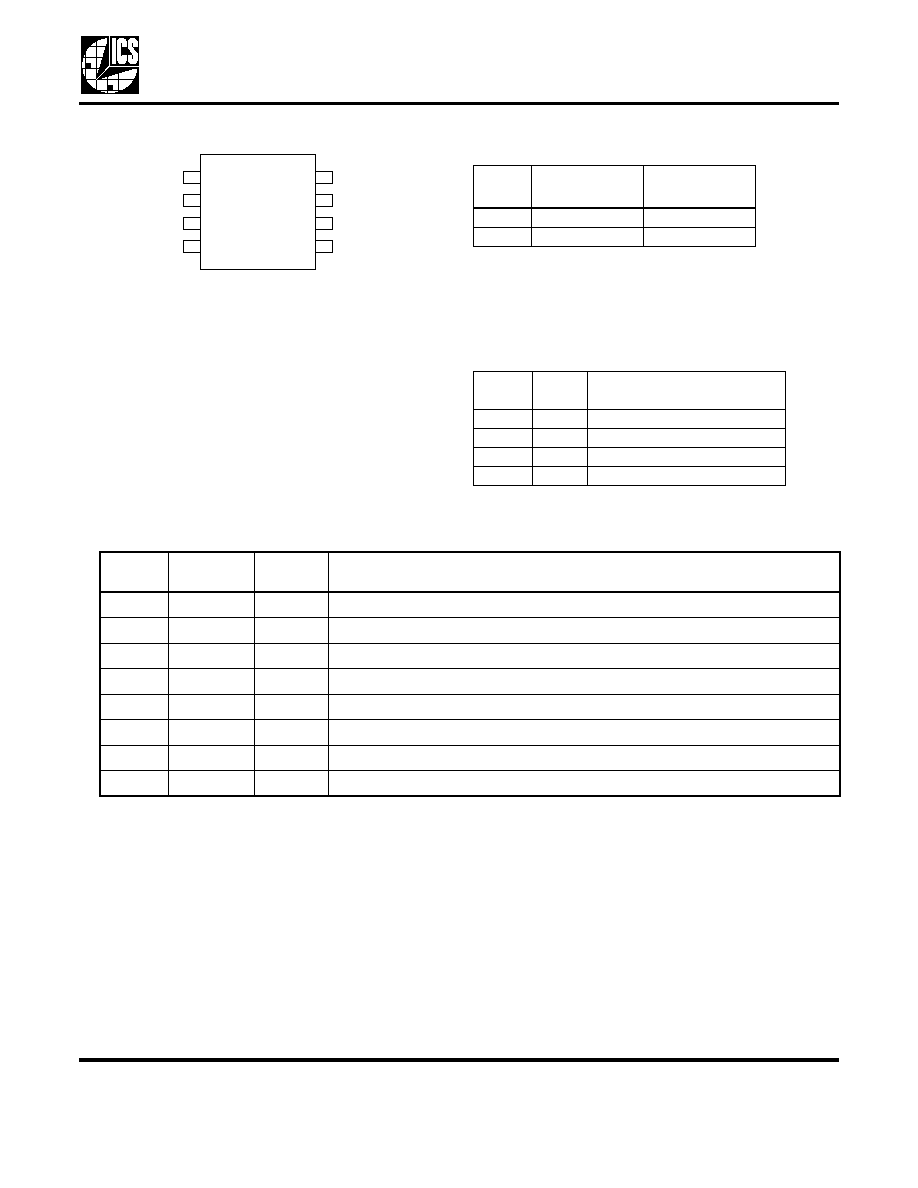
Block Diagram
PLL Clock
Synthesis
and Spread
Spectrum
Circuitry
SS%
CLK
GND
VDD
FS2:1
X1/CLKIN
X2
Clock Buffer/
Crystal
Oscillator
L
OW
EMI C
LOCK
G
ENERATOR
ICS180-01
MDS 180-01 B
2
Revision 050405
I n t e gra t e d C i r c u i t S y s t e m s
l
5 2 5 R a c e S t r e e t , S a n J o s e, C A 9 5 1 2 6
l
t e l ( 4 0 8 ) 2 9 7 - 1 2 0 1
l
w w w. i c s t . c o m
Pin Assignment
Spread Spectrum Select Table
0 = connect to GND
1 = connect directly to VDD
Note: SS% pin has an internal pull-up resistor
Frequency Range Selection Table
Pin Descriptions
1
2
3
X1/CLKIN
4
X2
GND
FS1
SS%
VDD
CLKOUT
8
7
6
5
FS2
8-pin (150 mil) SOIC
SS%
(Pin 4)
Spread
Direction
Spread
Percentage (%)
0
Down
-1.25%
1
Down
-3.75%
FS2
(Pin 8)
FS1
(Pin 7)
Frequency Range Selection
(MHz)
0
0
8-10
0
1
10-15
1
0
15-18
1
1
18-28
Pin
Number
Pin
Name
Pin Type
Pin Description
1
X1/CLKIN
Input
Crystal or Clock Input.
2
X2
Output
Crystal output. Float for a clock input.
3
GND
Power
Connect to ground.
4
SS%
Input
Select pin for spread amount. See table above. Internal pull-up resistor.
5
CLKOUT
Output
Spread spectrum clock output per table above.
6
VDD
Power
Connect to 3.3 V or 5 V.
7
FS1
Input
Select pin for input frequency. See table above. Internal pull-up resistor.
8
FS2
Input
Select pin for input frequency. See table above. Internal pull-up resistor.
L
OW
EMI C
LOCK
G
ENERATOR
ICS180-01
MDS 180-01 B
3
Revision 050405
I n t e gra t e d C i r c u i t S y s t e m s
l
5 2 5 R a c e S t r e e t , S a n J o s e, C A 9 5 1 2 6
l
t e l ( 4 0 8 ) 2 9 7 - 1 2 0 1
l
w w w. i c s t . c o m
External Components
The ICS180-01 requires a minimum number of external
components for proper operation.
Decoupling Capacitor
A decoupling capacitor of 0.01µF must be connected
between VDD and GND on pins 6 and 3, as close to
these pins as possible. For optimum device
performance, the decoupling capacitor should be
mounted on the component side of the PCB. Avoid the
use of vias in the decoupling circuit.
Series Termination Resistor
When the PCB trace between the clock output and the
load is over 1 inch, series termination should be used.
To series terminate a 50
trace (a commonly used
trace impedance) place a 33
resistor in series with
the clock line, as close to the clock output pin as
possible. The nominal impedance of the clock output is
20
.
value of these capacitors is given by the following
equation:
PCB Layout Recommendations
For optimum device performance and lowest output
phase noise, the following guidelines should be
observed.
1) The 0.01µF decoupling capacitor should be mounted
on the component side of the board as close to the
VDD pin as possible. No vias should be used between
the decoupling capacitor and VDD pin. The PCB trace
to VDD pin should be kept as short as possible, as
should the PCB trace to the ground via.
2) To minimize EMI, the 33
series termination resistor
(if needed) should be placed close to the clock output.
3) An optimum layout is one with all components on the
same side of the board, minimizing vias through other
signal layers. Other signal traces should be routed
away from the ICS180-01. This includes signal traces
just underneath the device, or on layers adjacent to the
ground plane layer used by the device.
Absolute Maximum Ratings
Stresses above the ratings listed below can cause permanent damage to the ICS180-01. These ratings,
which are standard values for ICS commercially rated parts, are stress ratings only. Functional operation of
the device at these or any other conditions above those indicated in the operational sections of the
specifications is not implied. Exposure to absolute maximum rating conditions for extended periods can
affect product reliability. Electrical parameters are guaranteed only over the recommended operating
temperature range.
Recommended Operation Conditions
Item
Rating
Supply Voltage, VDD
7 V
All Inputs and Outputs
-0.5 V to VDD+0.5 V
Ambient Operating Temperature (commercial)
0 to +70
∞C
Ambient Operating Temperature (industrial)
-40 to +85
∞C
Storage Temperature
-65 to +150
∞C
Junction Temperature
125
∞C
Soldering Temperature
260
∞C
Parameter
Min.
Typ.
Max.
Units
Ambient Operating Temperature
-40
+85
∞C
Power Supply Voltage (measured in respect to GND)
+3.135
+5.5
V

L
OW
EMI C
LOCK
G
ENERATOR
ICS180-01
MDS 180-01 B
4
Revision 050405
I n t e gra t e d C i r c u i t S y s t e m s
l
5 2 5 R a c e S t r e e t , S a n J o s e, C A 9 5 1 2 6
l
t e l ( 4 0 8 ) 2 9 7 - 1 2 0 1
l
w w w. i c s t . c o m
DC Electrical Characteristics
Unless stated otherwise, VDD = 3.3 V
±
5%, Ambient Temperature -40 to +85
∞C
Unless stated otherwise, VDD = 5 V,
±
10%, Ambient Temperature -40 to +85
∞C
Parameter
Symbol
Conditions
Min.
Typ.
Max.
Units
Operating Voltage
VDD
3.135
3.465
V
Supply Current
IDD
No load
18
32
mA
Input High Voltage
V
IH
2.4
V
Input Low Voltage
V
IL
0.8
V
Output High Voltage
V
OH
I
OH
= -4 mA
VDD-0.4
V
Output High Voltage
V
OH
I
OH
= -15 mA
2.4
V
Output Low Voltage
V
OL
I
OL
= 15 mA
0.4
V
Input Capacitance
C
IN
5
7
pF
Output Impedance
Rout
25
Input Pull-up Resistor
500
K
Power-up Time
First locked clock
cycle after steady
power
5
ms
Parameter
Symbol
Conditions
Min.
Typ.
Max.
Units
Operating Voltage
VDD
4.5
5
5.5
V
Supply Current
IDD
No load
30
50
mA
Input High Voltage
V
IH
0.7VDD
V
Input Low Voltage
V
IL
0.15VDD
V
Output High Voltage
V
OH
I
OH
= -24 mA
2.4
V
Output Low Voltage
V
OL
I
OL
= 24 mA
0.4
V
Output Impedance
Rout
20
ohms
Input Capacitance
C
IN
5
7
pF
Output Impedance
Rout
25
Input Pull-up Resistor
500
K
Power-up Time
First locked clock
cycle after steady
power
5
ms

L
OW
EMI C
LOCK
G
ENERATOR
ICS180-01
MDS 180-01 B
5
Revision 050405
I n t e gra t e d C i r c u i t S y s t e m s
l
5 2 5 R a c e S t r e e t , S a n J o s e, C A 9 5 1 2 6
l
t e l ( 4 0 8 ) 2 9 7 - 1 2 0 1
l
w w w. i c s t . c o m
AC Electrical Characteristics
Unless stated otherwise, VDD = 3.3 V±5% or 5 V±10%, Ambient Temperature -40 to +85
∞C, C
L
=15 pf
Note 1: Measured with 15 pF load
Thermal Characteristics
Parameter
Symbol
Conditions
Min.
Typ.
Max.
Units
Input/Output Frequency
8
28
MHz
Input Clock Duty Cycle
Time above VDD/2
40
60
%
Output Clock Duty Cycle
Note 1
40
50
60
%
Output Rise Time
t
OR
0.8 to 2.4 V, note 1
2
5
ns
Output Fall Time
t
OF
2.4 to 0.8 V, note 1
2
5
ns
Jitter
Cycle-to-cycle
250
300
ps
Parameter
Symbol
Conditions
Min.
Typ.
Max.
Units
Thermal Resistance Junction to
Ambient
JA
Still air
150
∞C/W
JA
1 m/s air flow
140
∞C/W
JA
3 m/s air flow
120
∞C/W
Thermal Resistance Junction to Case
JC
40
∞C/W