ICS1893AG, Rev. A 04/14/05
April, 2005
ICS reserves the right to make changes in the device data identified in
this publication without further notice. ICS advises its customers to
obtain the latest version of all device data to verify that any information
being relied upon by the customer is current and accurate.
Integrated Circuit Systems, Inc.
3.3 V 10Base-T/100Base-TX Integrated PHYceiver
TM
ICS1893AG
Document Type:
Data Sheet
Document Stage: Preliminary
Features
�
Single 3.3 V �10% power supply
�
Supports category 5 cables with attenuation in excess of
24dB at 100 MHz across a temperature range from 0�C to
+70�C. Industrial temperature version is also available.
�
DSP-based baseline wander correction to virtually
eliminate killer packets
�
Low-power, 0.35-micron CMOS (typically 400 mW)
�
Single-chip, fully integrated PHY provides PCS, PMA,
PMD, and AUTONEG sublayers of IEEE standard
�
10Base-T and 100Base-TX IEEE 802.3 compliant
�
Clock or crystal supported
�
Media Independent Interface (MII) supported
�
Managed or Unmanaged Applications
�
10M or 100M Half and Full Duplex Modes
�
Auto-Negotiation with Next Page. Parallel detection for
Legacy products
�
Fully integrated, DSP-based PMD includes:
� Adaptive equalization and baseline wander correction
� Transmit wave shaping and stream cipher scrambler
� MLT-3 encoder and NRZ/NRZI encoder
�
Loopback mode for Diagnostic Functions
�
Small footprint 56-pin 240 mil TSSOP package.
General
The ICS1893AG is a re-packaged version of the ICS1893AF
in a 56-lead TSSOP 240 mil package. The ICS1893AG is a
fully integrated, Physical Layer device (PHY) that is
compliant with both the 10Base-T and 100Base-TX
CSMA/CD Ethernet Standard, ISO/IEC 8802-3. The
ICS1893AG uses the same proven silicon as the
ICS1893AF but offers a smaller form factor solution to users
where physical package size is important.
All parametric specification and timing diagrams for the
ICS1893AF apply to the ICS1893AG. Refer to the
ICS1893AF datasheet for detailed specifications and timing.
The ICS1893AG uses the same twisted-pair transmit and
receive circuits as the ICS1893AF, and the same
recommended board layout techniques apply to the
ICS1893AG.
The ICS1893AG is intended for Node applications using the
standard MII interface to the MAC.
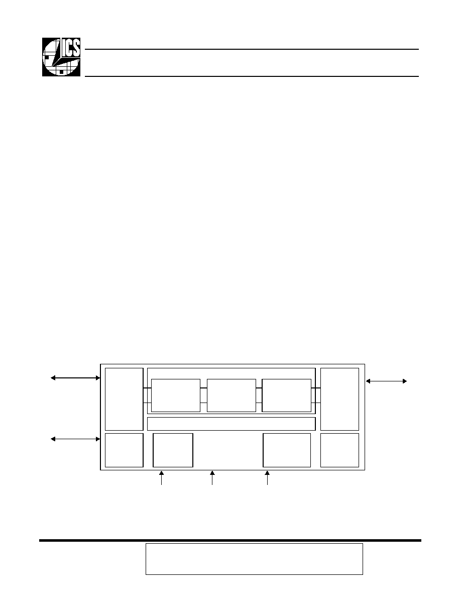
Clock
Power
LEDs and PHY
Address
Twisted-
Pair
Interface to
Magnetics
Modules and
RJ45
Connector
Integrated
Switch
MII
Extended
Register
Set
Interface
MUX
ICS1893AG Block Diagram
PCS
�
Framer
�
CRS/COL
Detection
�
Parallel to Serial
�
4B/5B
Auto-
Negotiation
10Base-T
100Base-TX
TP_PMD
�
MLT-3
�
Stream Cipher
�
Adaptive Equalizer
�
Baseline Wander
Correction
PMA
�
Clock Recovery
�
Link Monitor
�
Signal Detection
�
Error Detection
Low-Jitter
Clock
Synthesizer
Configuration
and Status
10/100 MII
MAC
Interface
MII
Management
Interface

ICS1893AG, Rev A 04/14/05
April, 2005
2
Table of Contents
ICS1893AG Data Sheet - Preliminary
Copyright � 2005, Integrated Circuit Systems, Inc.
All rights reserved.
Table of Contents
Section
Title
Page
Revision History
............................................................................................................................. 9
Chapter 1
Abbreviations and Acronyms ......................................................................................... 10
Chapter 2
Conventions and Nomenclature..................................................................................... 12
Chapter 3
Typical ICS1893AG Applications .................................................................................... 14
3.1
ICS1893AG / ICS1893AF Pin Differences..............................................................14
3.2
ICS1893AG / ICS1893AF Shared Features ...........................................................15
Chapter 4
Overview of the ICS1893AG ............................................................................................ 16
4.1 100Base-TX
Operation
..........................................................................................17
4.2 10Base-T
Operation
...............................................................................................17
Chapter 5
Operating Modes Overview............................................................................................. 18
5.1 Reset
Operations
...................................................................................................19
5.1.1 General
Reset
Operations
.....................................................................................19
5.1.2 Specific
Reset
Operations
.....................................................................................20
5.2 Power-Down
Operations
........................................................................................21
5.3 Automatic
Power-Saving
Operations
.....................................................................22
5.4 Auto-Negotiation
Operations
..................................................................................22
5.5 100Base-TX
Operations
........................................................................................23
5.6 10Base-T
Operations
.............................................................................................23
5.7
Half-Duplex and Full-Duplex Operations ...............................................................23
Chapter 6
Interface Overviews.......................................................................................................... 24
6.1
MII Data Interface ..................................................................................................25
6.2
Serial Management Interface .................................................................................26
6.3 Twisted-Pair
Interface
............................................................................................26
6.3.1 Twisted-Pair
Transmitter
Interface
.........................................................................27
6.3.2 Twisted-Pair
Receiver Interface .............................................................................28
6.4 Clock
Reference
Interface
.....................................................................................29
6.5 Status
Interface
......................................................................................................31
Chapter 7
Functional Blocks............................................................................................................. 33
7.1
Functional Block: Media Independent Interface .....................................................34
7.2
Functional Block: Auto-Negotiation ........................................................................35
7.2.1 Auto-Negotiation
General
Process
........................................................................36
7.2.2 Auto-Negotiation:
Parallel Detection ......................................................................37
7.2.3
Auto-Negotiation: Remote Fault Signaling .............................................................37
7.2.4 Auto-Negotiation:
Reset
and Restart .....................................................................38
7.2.5 Auto-Negotiation:
Progress Monitor .......................................................................38

Table of Contents
ICS1893AG, Rev. A 04/14/05
April, 2005
3
ICS1893AG Data Sheet - Preliminary
Copyright � 2005, Integrated Circuit Systems, Inc.
All rights reserved.
Table of Contents
Section
Title
Page
7.3
Functional Block: 100Base-X PCS and PMA Sublayers ........................................40
7.3.1 PCS
Sublayer
........................................................................................................40
7.3.2 PMA
Sublayer
........................................................................................................40
7.3.3
PCS/PMA Transmit Modules .................................................................................41
7.3.4
PCS/PMA Receive Modules ..................................................................................42
7.3.5
PCS Control Signal Generation .............................................................................43
7.3.6 4B/5B
Encoding/Decoding
.....................................................................................43
7.4
Functional Block: 100Base-TX TP-PMD Operations .............................................44
7.4.1 100Base-TX
Operation:
Stream Cipher Scrambler/Descrambler ..........................44
7.4.2
100Base-TX Operation: MLT-3 Encoder/Decoder .................................................44
7.4.3
100Base-TX Operation: DC Restoration ................................................................44
7.4.4
100Base-TX Operation: Adaptive Equalizer ..........................................................45
7.4.5
100Base-TX Operation: Twisted-Pair Transmitter .................................................45
7.4.6
100Base-TX Operation: Twisted-Pair Receiver .....................................................45
7.4.7
100Base-TX Operation: Auto Polarity Correction ..................................................46
7.4.8
100Base-TX Operation: Isolation Transformer ......................................................46
7.5
Functional Block: 10Base-T Operations ................................................................47
7.5.1
10Base-T Operation: Manchester Encoder/Decoder .............................................47
7.5.2
10Base-T Operation: Clock Synthesis ...................................................................47
7.5.3
10Base-T Operation: Clock Recovery ...................................................................47
7.5.4
10Base-T Operation: Idle .......................................................................................48
7.5.5
10Base-T Operation: Link Monitor .........................................................................48
7.5.6
10Base-T Operation: Smart Squelch .....................................................................49
7.5.7
10Base-T Operation: Carrier Detection .................................................................49
7.5.8
10Base-T Operation: Collision Detection ...............................................................49
7.5.9
10Base-T Operation: Jabber ..................................................................................50
7.5.10 10Base-T
Operation: SQE Test .............................................................................50
7.5.11 10Base-T
Operation: Twisted-Pair Transmitter .....................................................51
7.5.12 10Base-T
Operation: Twisted-Pair Receiver .........................................................51
7.5.13 10Base-T
Operation: Auto Polarity Correction .......................................................51
7.5.14 10Base-T
Operation: Isolation Transformer ...........................................................51
7.6
Functional Block: Management Interface ...............................................................52
7.6.1
Management Register Set Summary .....................................................................52
7.6.2
Management Frame Structure ...............................................................................52

ICS1893AG, Rev A 04/14/05
April, 2005
4
Table of Contents
ICS1893AG Data Sheet - Preliminary
Copyright � 2005, Integrated Circuit Systems, Inc.
All rights reserved.
Table of Contents
Section
Title
Page
Chapter 8
Management Register Set ............................................................................................... 55
8.1
Introduction to Management Register Set .............................................................56
8.1.1
Management Register Set Outline .........................................................................56
8.1.2
Management Register Bit Access ..........................................................................57
8.1.3
Management Register Bit Default Values ..............................................................57
8.1.4
Management Register Bit Special Functions .........................................................58
8.2
Register 0: Control Register ...................................................................................59
8.2.1
Reset (bit 0.15) ......................................................................................................59
8.2.2
Loopback Enable (bit 0.14) ....................................................................................60
8.2.3
Data Rate Select (bit 0.13) .....................................................................................60
8.2.4
Auto-Negotiation Enable (bit 0.12) .........................................................................60
8.2.5
Low Power Mode (bit 0.11) ....................................................................................61
8.2.6 Isolate
(bit
0.10)
.....................................................................................................61
8.2.7
Restart Auto-Negotiation (bit 0.9) ..........................................................................61
8.2.8
Duplex Mode (bit 0.8) .............................................................................................62
8.2.9
Collision Test (bit 0.7) ............................................................................................62
8.2.10
IEEE Reserved Bits (bits 0.6:0) .............................................................................62
8.3
Register 1: Status Register ....................................................................................63
8.3.1 100Base-T4
(bit
1.15)
............................................................................................63
8.3.2
100Base-TX Full Duplex (bit 1.14) .........................................................................64
8.3.3
100Base-TX Half Duplex (bit 1.13) ........................................................................64
8.3.4 10Base-T
Full Duplex (bit 1.12) .............................................................................64
8.3.5
10Base-T Half Duplex (bit 1.11) .............................................................................64
8.3.6
IEEE Reserved Bits (bits 1.10:7) ...........................................................................65
8.3.7
MF Preamble Suppression (bit 1.6) .......................................................................65
8.3.8 Auto-Negotiation
Complete (bit 1.5) .......................................................................65
8.3.9
Remote Fault (bit 1.4) ............................................................................................66
8.3.10
Auto-Negotiation Ability (bit 1.3) ............................................................................66
8.3.11
Link Status (bit 1.2) ................................................................................................67
8.3.12
Jabber Detect (bit 1.1) ...........................................................................................67
8.3.13
Extended Capability (bit 1.0) ..................................................................................67
8.4
Register 2: PHY Identifier Register ........................................................................68

Table of Contents
ICS1893AG, Rev. A 04/14/05
April, 2005
5
ICS1893AG Data Sheet - Preliminary
Copyright � 2005, Integrated Circuit Systems, Inc.
All rights reserved.
Table of Contents
Section
Title
Page
8.5
Register 3: PHY Identifier Register ........................................................................70
8.5.1
OUI bits 19-24 (bits 3.15:10) ..................................................................................70
8.5.2
Manufacturer's Model Number (bits 3.9:4) .............................................................71
8.5.3
Revision Number (bits 3.3:0) .................................................................................71
8.6
Register 4: Auto-Negotiation Register ...................................................................72
8.6.1
Next Page (bit 4.15) ...............................................................................................72
8.6.2
IEEE Reserved Bit (bit 4.14) ..................................................................................72
8.6.3
Remote Fault (bit 4.13) ..........................................................................................73
8.6.4
IEEE Reserved Bits (bits 4.12:10) .........................................................................73
8.6.5
Technology Ability Field (bits 4.9:5) .......................................................................74
8.6.6
Selector Field (Bits 4.4:0) .......................................................................................75
8.7
Register 5: Auto-Negotiation Link Partner Ability Register ....................................76
8.7.1
Next Page (bit 5.15) ...............................................................................................76
8.7.2 Acknowledge
(bit
5.14)
..........................................................................................77
8.7.3
Remote Fault (bit 5.13) ..........................................................................................77
8.7.4
Technology Ability Field (bits 5.12:5) .....................................................................77
8.7.5
Selector Field (bits 5.4:0) .......................................................................................77
8.8
Register 6: Auto-Negotiation Expansion Register ..................................................78
8.8.1
IEEE Reserved Bits (bits 6.15:5) ...........................................................................78
8.8.2
Parallel Detection Fault (bit 6.4) .............................................................................79
8.8.3
Link Partner Next Page Able (bit 6.3) ....................................................................79
8.8.4
Next Page Able (bit 6.2) .........................................................................................79
8.8.5
Page Received (bit 6.1) .........................................................................................79
8.8.6 Link
Partner
Auto-Negotiation Able (bit 6.0) ..........................................................79
8.9
Register 7: Auto-Negotiation Next Page Transmit Register ...................................80
8.9.1
Next Page (bit 7.15) ...............................................................................................81
8.9.2
IEEE Reserved Bit (bit 7.14) ..................................................................................81
8.9.3
Message Page (bit 7.13) ........................................................................................81
8.9.4
Acknowledge 2 (bit 7.12) .......................................................................................81
8.9.5
Toggle (bit 7.11) .....................................................................................................81
8.9.6
Message Code Field / Unformatted Code Field (bits 7.10:0) .................................81
8.10
Register 8: Auto-Negotiation Next Page Link Partner Ability Register ...................82
8.10.1
Next Page (bit 8.15) ...............................................................................................83
8.10.2
IEEE Reserved Bit (bit 8.14) ..................................................................................83
8.10.3
Message Page (bit 8.13) ........................................................................................83
8.10.4
Acknowledge 2 (bit 8.12) .......................................................................................83
8.10.5
Message Code Field / Unformatted Code Field (bits 8.10:0) .................................83