 | –≠–ª–µ–∫—Ç—Ä–æ–Ω–Ω—ã–π –∫–æ–º–ø–æ–Ω–µ–Ω—Ç: 2049-34 | –°–∫–∞—á–∞—Ç—å:  PDF PDF  ZIP ZIP |

MK2049-34
3.3 V Communications Clock PLL
MDS 2049-34 D
1
Revision 091801
Integrated Circuit Systems, Inc. ∑ 525 Race Street ∑ San Jose ∑ CA ∑ 95126 ∑ (408)295-9800tel∑ www.icst.com
∑ Packaged in 20 pin SOIC
∑ 3.3 V ±5% operation
∑ Fixed I/O phase relationship on all selections
∑ Meets the TR62411, ETS300 011, and GR-1244
specification for MTIE, Pull-in/Hold-in Range,
Phase Transients, and Jitter Generation for
Stratum 3, 4, and 4E
∑ Accepts multiple inputs: 8 kHz backplane clock,
Loop Timing frequencies, or 10-36 MHz
∑ Locks to 8 kHz ±100 ppm (External mode)
∑ Buffer Mode allows jitter attenuation of
10≠36 MHz input and x1/x0.5 or x2/x4 outputs
∑ Exact internal ratios enable zero ppm error
∑ Output clock rates include T1, E1, T3, E3, ISDN,
xDSL, and OC3 submultiples
∑ See the MK2049-01, -02, and -03 for more
selections at VDD = 5 V
The MK2049-34 is a Phase-Locked Loop (PLL) based
clock synthesizer that accepts multiple input
frequencies. With an 8 kHz clock input as a reference,
the MK2049-34 generates T1, E1, T3, E3, ISDN,
xDSL, and other communications frequencies. This
allows for the generation of clocks frequency-locked
and phase-locked to an 8 kHz backplane clock,
simplifying clock synchronization in communications
systems. The MK2049-34 can also accept a T1 or E1
input clock and provide the same output for loop
timing. All outputs are frequency locked together and
to the input.
This part also has a jitter-attenuated Buffer capability. In
this mode, the MK2049-34 is ideal for filtering jitter
from 27 MHz video clocks or other clocks with high
jitter.
ICS/MicroClock can customize these devices for many
other different frequencies. Contact your
ICS/MicroClock representative for more details.
Block Diagram
Description
Features
VDD
GND
PLL
Clock
Synthesis,
Control, and
Jitter
Attenuation
Circuitry
Output
Buffer
Output
Buffer
External/
Loop Timing
Mux
FS3:0
CAP1
CAP2
CLK
CLK/2
Output
Buffer
8 kHz
(External
Mode only)
Crystal
Oscillator
Reference
Crystal
X1
X2
4
3
3
RES
FCAP
ICLK
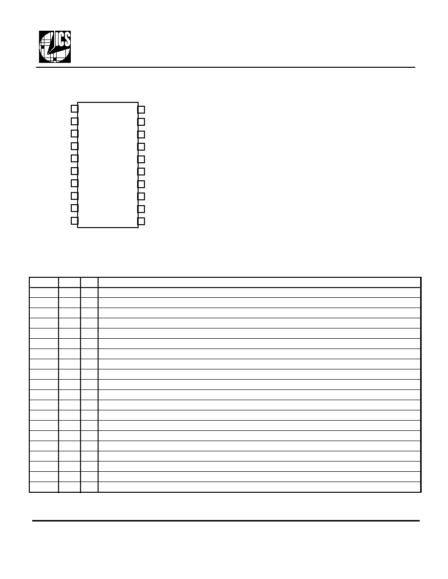
MK2049-34
3.3 V Communications Clock PLL
MDS 2049-34 D
2
Revision 091801
Integrated Circuit Systems, Inc. ∑ 525 Race Street ∑ San Jose ∑ CA ∑ 95126 ∑ (408)295-9800tel∑ www.icst.com
Pin Descriptions
Type:
XI, XO = crystal connections, I = Input, O = output, P = power supply connection, LF = loop filter
connections
Pin Assignment
20 pin (300 mil) SOIC
1
16
2
3
4
15
14
13
VDD
GND
X2
VDD
GND
5
6
7
8
12
11
10
9
FS3
X1
FS1
FS0
CAP1
ICLK
8K
CLK/2
CLK
18
17
19
20
FCAP
VDD
FS2
GND
CAP2
RES
Number Name Type Description
1
FS1
I
Frequency Select 1. Determines CLK input/outputs per tables on page 4.
2
X2
XO Crystal connection. Connect to a MHz crystal as shown in the tables on page 4.
3
X1
XI
Crystal connection. Connect to a MHz crystal as shown in the tables on page 4.
4
VDD
P
Connect to +3.3V.
5
FCAP
-
Filter Capacitor. Connect a 1000 pF ceramic capacitor to ground.
6
VDD
P
Connect to +3.3V.
7
GND
P
Connect to ground.
8
CLK
O
Clock output determined by status of FS3:0 per tables on page 4.
9
CLK/2
O
Clock output determined by status of FS3:0 per tables on page 4. Always 1/2 of CLK.
10
8K
O
Recovered 8 kHz clock output.
11
FS2
I
Frequency Select 2. Determines CLK input/outputs per tables on page 4.
12
FS3
I
Frequency Select 3. Determines CLK input/outputs per tables on page 4.
13
ICLK
I
Input clock connection. Connect to 8 kHz backplane or MHz clock.
14
GND
P
Connect to ground.
15
VDD
P
Connect to +3.3V.
16
CAP1
LF
Connect the loop filter ceramic capacitors and resistor between this pin and CAP2.
17
GND
P
Connect to ground.
18
CAP2
LF
Connect the loop filter ceramic capacitors and resistor between this pin and CAP1.
19
RES
-
Connect a 10-200k
resistor to ground. Contact ICS at 408-297-1201 for recommended value for your app.
20
FS0
I
Frequency Select 0. Determines CLK input/outputs per tables on page 4.

MK2049-34
3.3 V Communications Clock PLL
MDS 2049-34 D
3
Revision 091801
Integrated Circuit Systems, Inc. ∑ 525 Race Street ∑ San Jose ∑ CA ∑ 95126 ∑ (408)295-9800tel∑ www.icst.com
Parameter
Conditions
Minimum
Typical
Maximum
Units
ABSOLUTE MAXIMUM RATINGS (Note 1)
ABSOLUTE MAXIMUM RATINGS (Note 1)
Supply Voltage, VDD
Referenced to GND
7
V
Inputs and Clock Outputs
-0.5
VDD+0.5
V
Ambient Operating Temperature
MK2049-34SI
-40
85
∞C
Soldering Temperature
Max of 10 seconds
250
∞C
Storage Temperature
-65
150
∞C
DC CHARACTERISTICS (VDD = 3.3 V unless noted)
DC CHARACTERISTICS (VDD = 3.3 V unless noted)
Operating Voltage, VDD
3.15
3.3
3.45
V
Input High Voltage, VIH
2
V
Input Low Voltage, VIL
0.8
V
Output High Voltage, VOH, CMOS level
IOH=-4 mA
VDD-0.4
V
Output High Voltage, VOH
IOH=-8 mA
2.4
V
Output Low Voltage
IOL=8 mA
0.4
V
Operating Supply Current, IDD
No Load, VDD=3.3V
7
mA
Short Circuit Current
Each output
±50
mA
Input Capacitance, FS3:0
5
pF
AC CHARACTERISTICS (VDD = 3.3 V unless noted)
AC CHARACTERISTICS (VDD = 3.3 V unless noted)
Input Frequency, External Mode, Note 2
ICLK
8.000
kHz
Input Clock Pulse Width
10
ns
Propagation Delay
ICLK to CLK
0
6
ns
Output-Output Skew
CLK to CLK/2
150
ps
Output Clock Rise Time
0.8 to 2.0 V
2
ns
Output Clock Fall Time
2.0 to 0.8 V
2
ns
Output Clock Duty Cycle, High Time
At VDD/2, except 8K
40
60
%
Actual mean frequency error versus target
Any clock selection
0
0
ppm
Notes:
1. Stresses beyond those listed under Absolute Maximum Ratings could cause permanent damage to the device.
Prolonged exposure to levels above the operating limits but below the Absolute Maximums may affect device
reliability.
2. For loop timing modes and buffer modes, see tables on page 2 for required input clock frequencies.
Electrical Specifications
MK2049-34
3.3 V Communications Clock PLL
MDS 2049-34 D
4
Revision 091801
Integrated Circuit Systems, Inc. ∑ 525 Race Street ∑ San Jose ∑ CA ∑ 95126 ∑ (408)295-9800tel∑ www.icst.com
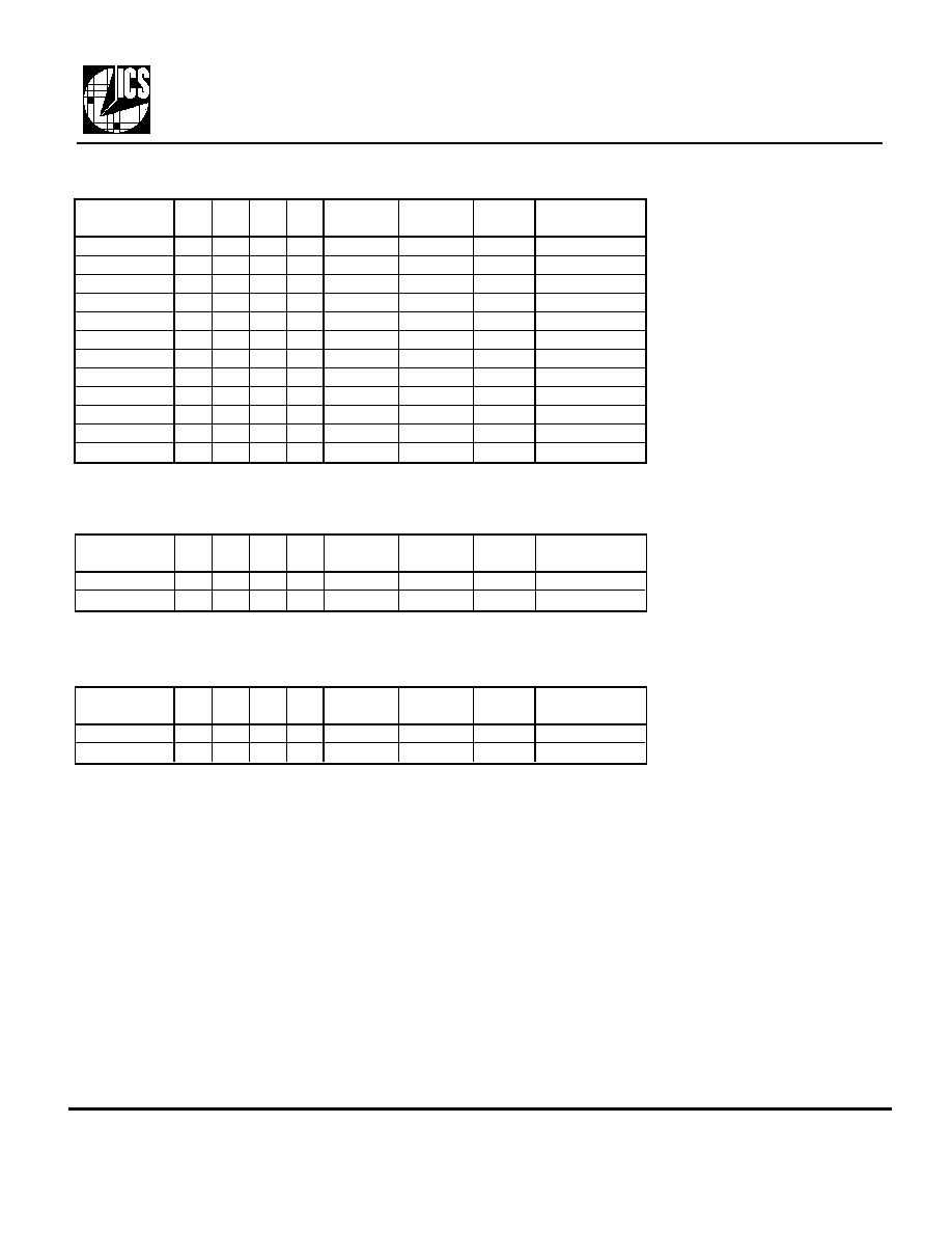
∑ 0 = connect directly to ground, 1 = connect directly to VDD.
∑ Crystal is connected to pins 2 and 3; clock input is applied to pin 13.
MK2049-34 Output Decoding Table ≠ External Mode (MHz)
ICLK
F S 3 F S 2 F S 1 F S 0
C L K / 2
CLK
8 K
Crystal
8 kHz
0
0
0
0
1.544
3.088
8 kHz
12.352
8 kHz
0
0
0
1
2.048
4.096
8 kHz
12.288
8 kHz
0
0
1
0
22.368
44.736
8 kHz
11.184
8 kHz
0
0
1
1
17.184
34.368
8 kHz
11.456
8 kHz
0
1
0
0
19.44
38.88
8 kHz
9.72
8 kHz
0
1
0
1
16.384
32.768
8 kHz
8.192
8 kHz
0
1
1
0
17.664
35.328
8 kHz
17.664
8 kHz
0
1
1
1
18.688
37.376
8 kHz
9.344
8 kHz
1
0
1
0
7.68
15.36
8 kHz
15.36
8 kHz
1
0
1
1
10.752
21.504
8 kHz
10.752
8 kHz
1
1
0
0
10.24
20.48
8 kHz
10.24
8 kHz
1
1
0
1
38.88
77.76
8 kHz
9.72
ICLK
F S 3 F S 2 F S 1 F S 0
C L K / 2
CLK
8 K
Crystal
1.544
1
0
0
0
1.544
3.088
N/A
12.352
2.048
1
0
0
1
2.048
4.096
N/A
12.288
MK2049-34 Output Decoding Table ≠ Loop Timing Mode (MHz)
ICLK
F S 3 F S 2 F S 1 F S 0
C L K / 2
CLK
8 K
Crystal
19 - 36
1
1
1
0
ICLK/2
ICLK
N/A
ICLK/2
10 - 18
1
1
1
1
2*ICLK
4*ICLK
N/A
ICLK
MK2049-34 Output Decoding Table ≠ Buffer Mode (MHz)

MK2049-34
3.3 V Communications Clock PLL
MDS 2049-34 D
5
Revision 091801
Integrated Circuit Systems, Inc. ∑ 525 Race Street ∑ San Jose ∑ CA ∑ 95126 ∑ (408)295-9800tel∑ www.icst.com
OPERATING MODES
The MK2049-34 has three operating modes: External, Loop Timing, and Buffer. Although each mode uses an
input clock to generate various output clocks, there are important differences in their input and crystal requirements.
External Mode
The MK2049-34 accepts an external 8 kHz clock and will produce a number of common communication clock
frequencies. The 8 kHz input clock does not need to have a 50% duty cycle; a "high" or "on" pulse as narrow as 10
ns is acceptable. In the MK2049-34, the rising edges of CLK and CLK/2 are both aligned with the rising edge of the
8 kHz ICLK; refer to Figure 1 for more details.
Loop Timing Mode
This mode can be used to remove the jitter from standard high-frequency communication clocks. For T1 and E1
inputs, the CLK/2 output will be the same as the input frequency, with CLK at twice the input frequency.
Buffer Mode
Unlike the other two modes that accept only a single specified input frequency, Buffer Mode will accept a wider
range of input clocks. The input jitter is attenuated, and the outputs on CLK and CLK/2 also provide the option of
getting x1, x2, x4, or 1/2 of the input frequency. For example, this mode can be used to remove the jitter from a 27
MHz clock, generating low-jitter 27 MHz and 13.5 MHz outputs.
INPUT AND OUTPUT SYNCHRONIZATION
As shown in the tables on page 4, the MK2049-34 offers a Zero Delay feature in all selections. There is an internal
feedback path between ICLK and the output clocks, providing a fixed phase relationship between the input and
output, a requirement in many communications systems.
The rising edge of ICLK will be aligned with the rising edges of CLK and CLK/2. (8 kHz is used in this illustration, but
the same is true for the selections in the Loop Timing and Buffer modes.)
ICLK (8 kHz)
CLK (MHz)
CLK/2(MHz)
Figure 1. MK2049-34 Input and Output Clock Waveforms