 | –≠–ª–µ–∫—Ç—Ä–æ–Ω–Ω—ã–π –∫–æ–º–ø–æ–Ω–µ–Ω—Ç: 21G5L | –°–∫–∞—á–∞—Ç—å:  PDF PDF  ZIP ZIP |

ICS421-05
MDS 421-05 B
1
Revision 072304
Integrated Circuit Systems
525 Race Street, San Jose, CA 95126
tel (408) 297-1201
www.icst.com
D
IGITAL
V
IDEO
C
AMERA
C
LOCK
Description
The ICS421-05 is a low-power, low-jitter clock
synthesizer developed for digital camera applications.
The device accepts a 27 MHz input clock to support
common digital video camera interface frequencies
including a 12 MHz for USB, 24.576 MHz for
IEEE1394, and a 72 MHz CCD clock. Power
consumption was minimized by lowering the voltage
requirement to 1.8 V minimum.
The ICS421-05 utilizes a small form factor 8-pin
TSSOP package.
ICS is a leader in low power, consumer application
clock sources. Devices are capable of supporting CCD,
video, audio, USB, CPU, and other peripherals.
Features
∑
Ultra-low operating voltage from 1.8 V to 2.4 V
∑
10 mA supply current
∑
27 MHz input clock frequency
∑
Fixed 24.576 MHz clock supports IEEE1394
∑
Fixed 12 MHz clock supports USB
∑
Fixed 72 MHz CCD clock
∑
Packaged in 8-pin TSSOP (Pb free)
Block Diagram
Clock
Buffer
CLKIN
27 MHz
Input Clock
IEEE
PLL
12M
24.576M
VDD
GND
CCD/
USB
PLL
72M
OE_USB
1
2

D
IGITAL
V
IDEO
C
AMERA
C
LOCK
MDS 421-05 B
2
Revision 072304
Integrated Circuit Systems
525 Race Street, San Jose, CA 95126
tel (408) 297-1201
www.icst.com
ICS421-05
Pin Assignment
OE_USB Operation Table
Pin Descriptions
External Components
Series Termination Resistor
Clock output traces over one inch should use series
termination. To series terminate a 50
trace (a
commonly used trace impedance), place a 33
resistor
in series with the clock line, as close to the clock output
pin as possible. The nominal impedance of the clock
output is 20
.
Decoupling Capacitor
As with any high-performance mixed-signal IC, the
ICS421-05 must be isolated from system power supply
noise to perform optimally.
A decoupling capacitor of 0.01µF must be connected
between VDD and the PCB ground plane.
PCB Layout Recommendations
For optimum device performance and lowest output
phase noise, the following guidelines should be
observed.
1) The 0.01µF decoupling capacitor should be mounted
on the component side of the board as close to the
VDD pin as possible. No vias should be used between
decoupling capacitor and VDD pin. The PCB trace to
VDD pin should be kept as short as possible, as should
the PCB trace to the ground via. Distance of the ferrite
bead and bulk decoupling from the device is less
critical.
2) To minimize EMI, the 33
series termination resistor
(if needed) should be placed close to the clock output.
3) An optimum layout is one with all components on the
same side of the board, minimizing vias through other
signal layers (the ferrite bead and bulk decoupling
capacitor can be mounted on the back). Other signal
traces should be routed away from the ICS421-05. This
includes signal traces just underneath the device, or on
layers adjacent to the ground plane layer used by the
device.
1
2
3
CLKIN
4
VDD
GND
12M
24.576M
VDD
72M
8
7
6
5
OE_USB
8 pin (173 mil) TSSOP
OE_USB
Function
0
Output tri-state
1
Output running
Pin
Number
Pin
Name
Pin
Type
Pin Description
1
CLKIN
Input
27 MHz single ended clock input.
2
VDD
Power
Connect to voltage supply.
3
GND
Power
Connect to ground.
4
24.576M
Output
24.576 MHz clock output.
5
72M
Output
72 MHz clock output for CCD.
6
VDD
Power
Connect to voltage supply.
7
12M
Output
12 MHz clock output for USB.
8
OE_USB
Input
Output enable for 12M clock for USB. See table for functionality,
internal pull-down.

D
IGITAL
V
IDEO
C
AMERA
C
LOCK
MDS 421-05 B
3
Revision 072304
Integrated Circuit Systems
525 Race Street, San Jose, CA 95126
tel (408) 297-1201
www.icst.com
ICS421-05
Absolute Maximum Ratings
Stresses above the ratings listed below can cause permanent damage to the ICS421-05. These ratings,
which are standard values for ICS commercially rated parts, are stress ratings only. Functional operation of
the device at these or any other conditions above those indicated in the operational sections of the
specifications is not implied. Exposure to absolute maximum rating conditions for extended periods can
affect product reliability. Electrical parameters are guaranteed only over the recommended operating
temperature range.
Recommended Operating Conditions
DC Electrical Characteristics
VDD = 1.8 V to 2.4 V
, Ambient Temperature 0 to +70
∞
C, unless stated otherwise
Item
Rating
Supply Voltage, VDD
-0.5 V to 7 V
All Inputs and Outputs
-0.5 V to VDD +0.5 V
Ambient Operating Temperature
0 to +70
∞
C
Storage Temperature
-65 to +150
∞
C
Junction Temperature
125
∞
C
Soldering Temperature
260
∞
C
Parameter
Min.
Typ.
Max.
Units
Ambient Operating Temperature
0
≠
+70
∞
C
Power Supply Voltage (measured in respect to GND)
+1.8
+2.4
V
Parameter
Symbol
Conditions
Min.
Typ.
Max.
Units
Operating Voltage
VDD
1.80
2.40
V
Input High Voltage
V
IH
CLKIN
VDD/2+0.5
V
Input Low Voltage
V
IL
CLKIN
VDD/2-0.5
V
Input High Voltage
V
IH
OE_USB pin
TBD
V
Input Low Voltage
V
IL
OE_USB pin
TBD
V
Output High Voltage
V
OH
VDD = 2.4 V,
I
OH
= -4 mA
1.9
V
Output Low Voltage
V
OL
VDD = 2.4 V,
I
OL
= 4 mA
0.4
V
Output High Voltage
V
OH
VDD = 1.8 V
I
OH
= -4 mA
1.4
V
Output Low Voltage
V
OL
VDD = 1.8 V
I
OL
= 4 mA
0.4
V
Operating Supply Current
IDD
No load, 3 out
10
mA
D
IGITAL
V
IDEO
C
AMERA
C
LOCK
MDS 421-05 B
4
Revision 072304
Integrated Circuit Systems
525 Race Street, San Jose, CA 95126
tel (408) 297-1201
www.icst.com
ICS421-05
Notes: 1. Nominal switching threshold is VDD/2
AC Electrical Characteristics
VDD = 1.8 V to 2.4 V
, Ambient Temperature 0 to +70
∞
C, unless stated otherwise
Thermal Characteristics
Marking Diagram
Notes:
1. ###### is the lot code.
2. YYWW is the last two digits of the year, and the week
number that the part was assembled.
3. "L" designates Pb (lead) free package.
Short Circuit Current
I
OS
Each output
50
mA
Nominal Output Impedance
Z
o
20
W
On-chip Pull-down Resistor
OE_USB
150
k
Parameter
Symbol
Conditions
Min.
Typ. Max. Units
Input Frequency
Clock Input
27
MHz
Output Rise Time
t
OR
VDD=2.4 V, 20% to
80%, C
L
=10 pF
1.8
ns
Output Fall Time
t
OF
VDD=2.4 V, 80% to
20%, C
L
=10 pF
1.8
ns
Output Rise Time
t
OR
VDD=1.8 V, 20% to
80%, C
L
=10 pF
2.5
ns
Output Fall Time
t
OF
VDD=1.8 V, 80% to
20%, C
L
=10 pF
2.5
ns
Output Clock Duty Cycle
at VDD/2
50
%
Absolute Pk-Pk Jitter
72 MHz output clock
±200
ps
PLL Lock Time within 1%
Power OFF to lock
10
ms
Parameter
Symbol
Conditions
Min.
Typ.
Max.
Units
Parameter
Symbol
Conditions
Min.
Typ.
Max. Units
Thermal Resistance Junction to
Ambient
JA
Still air
110
∞
C/W
JA
1 m/s air flow
100
∞
C/W
JA
3 m/s air flow
80
∞
C/W
Thermal Resistance Junction to Case
JC
35
∞
C/W
1
4
8
YYWW
21G5L
######
5

D
IGITAL
V
IDEO
C
AMERA
C
LOCK
MDS 421-05 B
5
Revision 072304
Integrated Circuit Systems
525 Race Street, San Jose, CA 95126
tel (408) 297-1201
www.icst.com
ICS421-05
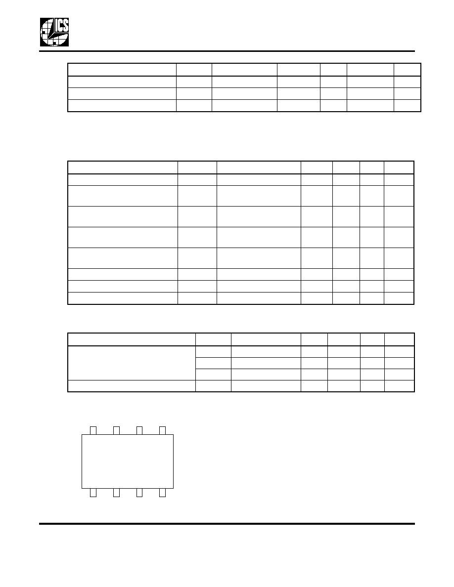
Package Outline and Package Dimensions (8-pin TSSOP, 173 Mil. Body)
Package dimensions are kept current with JEDEC Publication No. 95
Ordering Information
"LF" denotes Pb (lead) free package.
While the information presented herein has been checked for both accuracy and reliability, Integrated Circuit Systems (ICS)
assumes no responsibility for either its use or for the infringement of any patents or other rights of third parties, which would
result from its use. No other circuits, patents, or licenses are implied. This product is intended for use in normal commercial
applications. Any other applications such as those requiring extended temperature range, high reliability, or other extraordinary
environmental requirements are not recommended without additional processing by ICS. ICS reserves the right to change any
circuitry or specifications without notice. ICS does not authorize or warrant any ICS product for use in life support devices or
critical medical instruments.
Part / Order Number
Marking
Shipping Packaging
Package
Temperature
ICS421G-05LF
21G5L
Tubes
8-pin TSSOP
0 to +70
∞
C
ICS421G-05LFT
Tape & Reel
8-pin TSSOP
0 to +70
∞
C
INDEX
AREA
1
8
D
E1
E
SEATING
PLANE
A1
A
A2
e
- C -
b
aaa
C
c
L
Millimeters
Inches
Symbol
Min
Max
Min
Max
A
--
1.20
--
0.047
A1
0.05
0.15
0.002
0.006
A2
0.80
1.05
0.032
0.041
b
0.19
0.30
0.007
0.012
C
0.09
0.20
0.0035
0.008
D
2.90
3.10
0.114
0.122
E
6.40 BASIC
0.252 BASIC
E1
4.30
4.50
0.169
0.177
e
0.65 Basic
0.0256 Basic
L
0.45
0.75
0.018
0.030
0
∞
8
∞
0
∞
8
∞
aaa
--
0.10
--
0.004