 | –≠–ª–µ–∫—Ç—Ä–æ–Ω–Ω—ã–π –∫–æ–º–ø–æ–Ω–µ–Ω—Ç: 26G11 | –°–∫–∞—á–∞—Ç—å:  PDF PDF  ZIP ZIP |

ICS1726-11
MDS 1726-11 A
1
Revision 092905
Integrated Circuit Systems, Inc.
525 Race Street, San Jose, CA 95126
tel (408) 297-1201
www.icst.com
Low EMI Clock Generator
PRELIMINARY INFORMATION
Description
The ICS1726-11 generates a low EMI output clock
from a clock or crystal input. The part is designed to
dither the LCD interface clock for PDAs, printers,
scanners, modems, copiers, and others. Using ICS'
proprietary mix of analog and digital Phase-Locked
Loop (PLL) technology, the device spreads the
frequency spectrum of the output, reducing the
frequency amplitude peaks by several dB. The
ICS1726-11 offers both centered and down spread
from a high-speed clock input.
ICS offers many other clocks for computers and
computer peripherals. Consult us when you need to
remove crystals and oscillators from your board.
Features
∑
Packaged in 8-pin SOIC/TSSOP
∑
Provides a spread spectrum output clock
∑
Supports flat panel controllers
∑
Accepts a clock or crystal input (provides same
frequency dithered output)
∑
Input frequency range of 16 to 32 MHz
∑
Output frequency range of 16 to 32 MHz
∑
Center and down spread
∑
Peak reduction by 8 dB to 16 dB typical on 3rd
through 19th odd harmonics
∑
Low EMI feature can be disabled
∑
Includes power down
∑
Operating voltage of 3.3 V
∑
Advanced, low-power CMOS process
Block Diagram
PLL Clock
Synthesis
and Spread
Spectrum
Circuitry
X1
S1:0
SSCLK
2
GND
VDD
Clock Buffer/
Crystal
Ocsillator
X1/CLK
X2
External caps required for with crystal
for accurate tuning of the clock

Low EMI Clock Generator
MDS 1726-11 A
2
Revision 092905
Integrated Circuit Systems, Inc.
525 Race Street, San Jose, CA 95126
tel (408) 297-1201
www.icst.com
ICS1726-11
PRELIMINARY INFORMATION
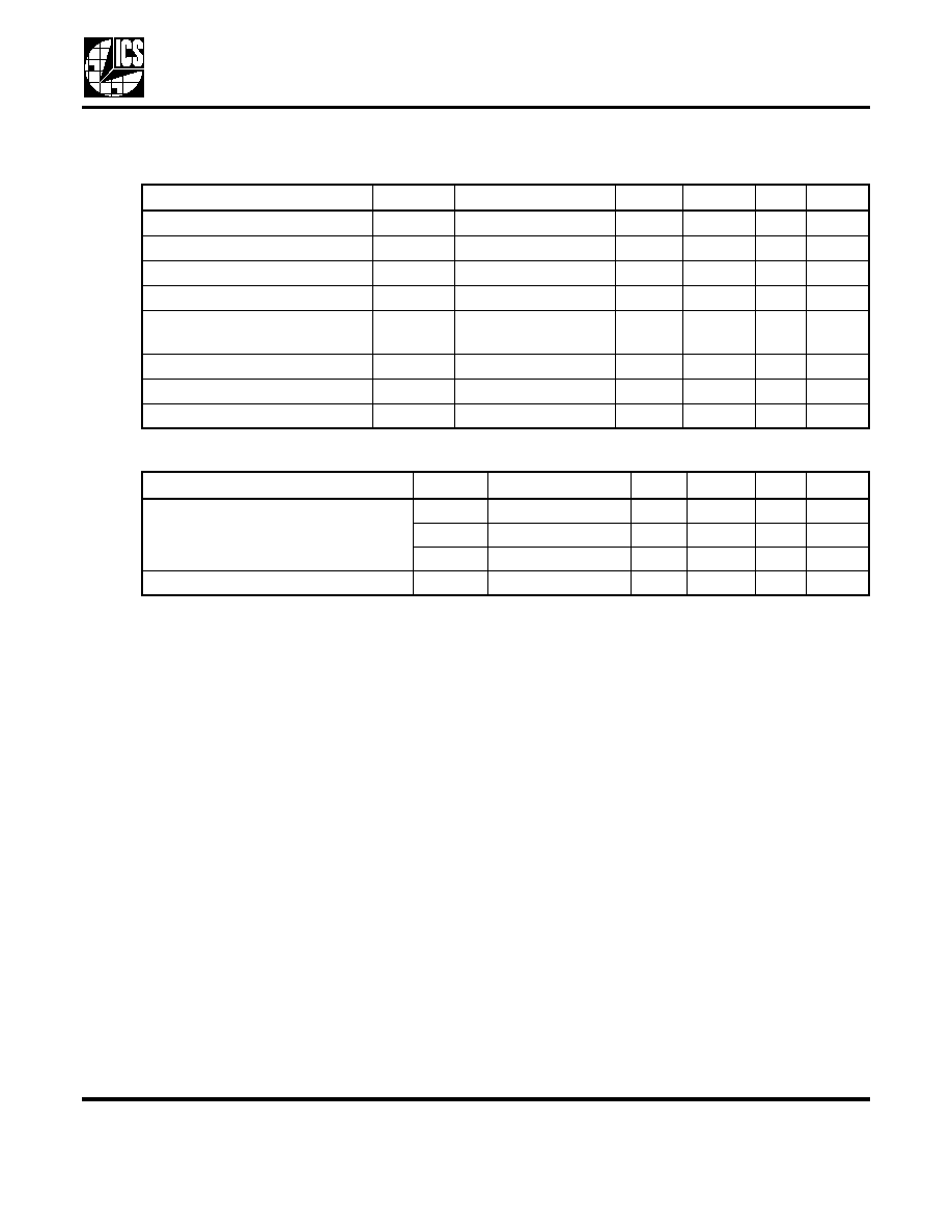
Pin Assignment
Spread Direction and Percentage
Select Table
0 = connect to GND
M = unconnected (floating)
1 = connect directly to VDD
Pin Descriptions
X1/ICLK
GND
S1
VDD
S0
NC
SSCLK
X2
1
2
3
4
8
7
6
5
8 pin (150 mil) SOIC
8-pin (173 mil) TSSOP
S1
Pin 3
S0
Pin 4
Spread
Direction
Spread
Percentage
0
0
Center
±1.4
0
M
Center
±1.1
0
1
Center
±0.6
M
0
Center
±0.5
M
M
No Spread
-
M
1
Down
-1.6
1
0
Down
-2.0
1
M
Down
-0.7
1
1
Down
-3.0
Pin
Number
Pin
Name
Pin Type
Pin Description
1
X1/ICLK
Input
Connect to a 16 to 32 MHz crystal or clock.
2
GND
Power
Connect to ground.
3
S1
Input
Function select 1 input. Selects spread amount and direction per table above.
(default-internal mid-level).
4
S0
Input
Function select 0 input. Selects spread amount and direction per table above.
(default-internal mid-level).
5
SSCLK
Output
Clock output with Spread spectrum.
6
NC
--
No connect. Do not connect this pin to anything.
7
VDD
Power
Connect to +3.3 V.
8
X2
XO
Crystal connection to a 16 to 32 MHz crystal. Leave unconnected for clock.

Low EMI Clock Generator
MDS 1726-11 A
3
Revision 092905
Integrated Circuit Systems, Inc.
525 Race Street, San Jose, CA 95126
tel (408) 297-1201
www.icst.com
ICS1726-11
PRELIMINARY INFORMATION
External Components
The ICS1726-11 requires a minimum number of
external components for proper operation.
Decoupling Capacitor
A decoupling capacitor of 0.01µF must be connected
between VDD and GND on pins 7 and 2, as close to
these pins as possible. For optimum device
performance, the decoupling capacitor should be
mounted on the component side of the PCB. Avoid the
use of vias in the decoupling circuit.
Series Termination Resistor
When the PCB trace between the clock output and the
load is over 1 inch, series termination should be used.
To series terminate a 50
trace (a commonly used
trace impedance) place a 33
resistor in series with
the clock line, as close to the clock output pin as
possible. The nominal impedance of the clock output is
20
.
Tri-level Select Pin Operation
The S1, S0 select pins are tri-level, meaning they have
three separate states to make the selections shown in
the table on page 2. To select the M (mid) level, the
connection to these pins must be eliminated by either
floating them, or tri-stating the driver connected to the
select pin.
PCB Layout Recommendations
For optimum device performance and lowest output
phase noise, the following guidelines should be
observed.
1) The 0.01µF decoupling capacitor should be mounted
on the component side of the board as close to the
VDD pin as possible. No vias should be used between
the decoupling capacitor and VDD pin. The PCB trace
to VDD pin should be kept as short as possible, as
should the PCB trace to the ground via.
2) To minimize EMI, the 33
series termination resistor
(if needed) should be placed close to the clock output.
3) An optimum layout is one with all components on the
same side of the board, minimizing vias through other
signal layers. Other signal traces should be routed
away from the ICS1726-11. This includes signal traces
just underneath the device, or on layers adjacent to the
ground plane layer used by the device.
Crystal Information
The crystal used should be a fundamental mode (do
not use third overtone), parallel resonant. Crystal
capacitors should be connected from pins X1 to ground
and X2 to ground to optimize the initial accuracy. The
value of these capacitors is given by the following
equation:
Crystal caps (pF) = (C
L
- 6) x 2
In the equation, C
L
is the crystal load capacitance. So,
for a crystal with a 16 pF load capacitance, two 20 pF
[(16-6) x 2] capacitors should be used.
Spread Spectrum Profile
The ICS1726-11 low EMI clock generator uses an
optimized frequency slew rate to facilitate down stream
tracking by zero delay buffers and other PLL devices.
The frequency modulation amplitude is constant
despite variations of the input frequency.
Time
F
r
eq
ue
nc
y
Modulation Rate

Low EMI Clock Generator
MDS 1726-11 A
4
Revision 092905
Integrated Circuit Systems, Inc.
525 Race Street, San Jose, CA 95126
tel (408) 297-1201
www.icst.com
ICS1726-11
PRELIMINARY INFORMATION
Absolute Maximum Ratings
Stresses above the ratings listed below can cause permanent damage to the ICS1726-11. These ratings,
which are standard values for ICS commercially rated parts, are stress ratings only. Functional operation of
the device at these or any other conditions above those indicated in the operational sections of the
specifications is not implied. Exposure to absolute maximum rating conditions for extended periods can
affect product reliability. Electrical parameters are guaranteed only over the recommended operating
temperature range.
Recommended Operation Conditions
DC Electrical Characteristics
Unless stated otherwise, VDD = 3.3 V, Ambient Temperature 0 to +70
∞C
Item
Rating
Supply Voltage, VDD
7 V
All Inputs and Outputs
-0.5 V to VDD+0.5 V
Ambient Operating Temperature
0 to +70
∞C
Storage Temperature
-65 to +150
∞C
Junction Temperature
125
∞C
Soldering Temperature
260
∞C
Parameter
Min.
Typ.
Max.
Units
Ambient Operating Temperature
0
+70
∞C
Power Supply Voltage (measured in respect to GND)
+3.0
3.6
V
Parameter
Symbol
Conditions
Min.
Typ.
Max.
Units
Operating Voltage
VDD
3.0
3.3
3.6
V
Supply Current
IDD
No load, at 3.3 V,
Fin=24 MHz
23
30
mA
No load, at 3.3 V,
Fin=32 MHz
35
mA
Input High Voltage
V
IH
0.85VDD
VDD
VDD
V
Input middle Voltage
V
IHM
0.4VDD
0.5VDD
0.6VDD
V
Input Low Voltage
V
IL
0.0
0.0
0.15VDD
V
Output High Voltage
V
OH
CMOS, I
OH
= -4 mA
2.4
V
Output High Voltage
V
OH
I
OH
= -6 mA
2.0
V
Output Low Voltage
V
OL
I
OL
= -4 mA
0.4
V
I
OL
= -10 mA
1.2
V
Input Capacitance
C
IN1
S0, S1, pins
4
6
pF
C
IN2
X1, X2 pins
6
9
pF
Low EMI Clock Generator
MDS 1726-11 A
5
Revision 092905
Integrated Circuit Systems, Inc.
525 Race Street, San Jose, CA 95126
tel (408) 297-1201
www.icst.com
ICS1726-11
PRELIMINARY INFORMATION
AC Electrical Characteristics
Unless stated otherwise, VDD = 3.3 V, Ambient Temperature 0 to +70
∞ C
Thermal Characteristics
Parameter
Symbol
Conditions
Min.
Typ.
Max.
Units
Input Clock Frequency
16
32
MHz
Output Clock Frequency
16
32
MHz
Input Clock Duty Cycle
Time above VDD/2
40
60
%
Output Clock Duty Cycle
Time above 1.5 V
45
50
55
%
Cycle to cycle Jitter
Fin=27 MHz,
Fout=27 MHz
200
450
ps
Output Rise Time
t
R
0.4 to 2.4 V
2.4
3.2
4.0
ns
Output Fall Time
t
F
2.4 to 0.4 V
2.4
3.2
4.0
ns
EMI Peak Frequency Reduction
8 to 16
dB
Parameter
Symbol
Conditions
Min.
Typ.
Max.
Units
Thermal Resistance Junction to
Ambient
JA
Still air
150
∞C/W
JA
1 m/s air flow
140
∞C/W
JA
3 m/s air flow
120
∞C/W
Thermal Resistance Junction to Case
JC
40
∞C/W

Low EMI Clock Generator
MDS 1726-11 A
6
Revision 092905
Integrated Circuit Systems, Inc.
525 Race Street, San Jose, CA 95126
tel (408) 297-1201
www.icst.com
ICS1726-11
PRELIMINARY INFORMATION
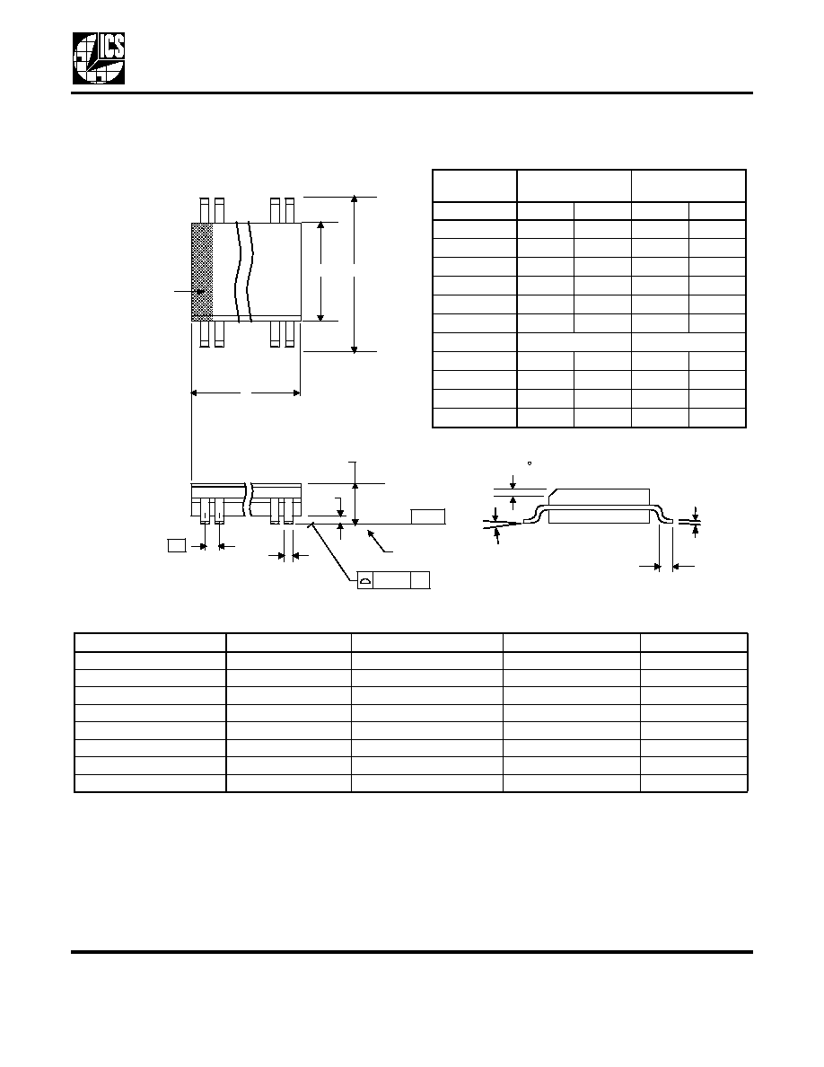
Package Outline and Package Dimensions
(8-pin TSSOP)
Package dimensions are kept current with JEDEC Publication No. 95
IN D E X
A R E A
1 2
8
D
E 1
E
S E A T IN G
P LA N E
A
1
A
A
2
e
- C -
b
a a a
C
c
L
Millimeters
Inches
Symbol
Min
Max
Min
Max
A
--
1.20
--
0.047
A1
0.05
0.15
0.002
0.006
A2
0.80
1.05
0.032
0.041
b
0.19
0.30
0.007
0.012
C
0.09
0.20
0.0035
0.008
D
2.90
3.10
0.114
0.122
E
6.40 BASIC
0.252 BASIC
E1
4.30
4.50
0.169
0.177
e
0.65 Basic
0.0256 Basic
L
0.45
0.75
0.018
0.030
0
∞
8
∞
0
∞
8
∞
aaa
-
0.10
-
0.004
Low EMI Clock Generator
MDS 1726-11 A
7
Revision 092905
Integrated Circuit Systems, Inc.
525 Race Street, San Jose, CA 95126
tel (408) 297-1201
www.icst.com
ICS1726-11
PRELIMINARY INFORMATION
Package Outline and Package Dimensions
(8-pin SOIC, 150 Mil. Body)
Package dimensions are kept current with JEDEC Publication No. 95
Ordering Information
Parts that are ordered with a "LF" suffix to the part number are the Pb-Free configuration and are RoHS compliant.
While the information presented herein has been checked for both accuracy and reliability, Integrated Circuit Systems (ICS)
assumes no responsibility for either its use or for the infringement of any patents or other rights of third parties, which would
result from its use. No other circuits, patents, or licenses are implied. This product is intended for use in normal commercial
applications. Any other applications such as those requiring extended temperature range, high reliability, or other extraordinary
environmental requirements are not recommended without additional processing by ICS. ICS reserves the right to change any
circuitry or specifications without notice. ICS does not authorize or warrant any ICS product for use in life support devices or
critical medical instruments.
Part / Order Number
Marking
Shipping Packaging
Package
Temperature
ICS1726G-11
26G11
Tubes
8-pin TSSOP
0 to +70
∞ C
ICS1726G-11T
26G11
Tape and Reel
8-pin TSSOP
0 to +70
∞ C
ICS1726G-11LF
26G11L
Tubes
8-pin TSSOP
0 to +70
∞ C
ICS1726G-11LFT
26G11L
Tape and Reel
8-pin TSSOP
0 to +70
∞ C
ICS1726M-11
1726M11
Tubes
8-pin SOIC
0 to +70
∞ C
ICS1726M-11T
1726M11
Tape and Reel
8-pin SOIC
0 to +70
∞ C
ICS1726M-11LF
1726M11L
Tubes
8-pin SOIC
0 to +70
∞ C
ICS1726M-11LFT
1726M11L
Tape and Reel
8-pin SOIC
0 to +70
∞ C
INDEX
AREA
1 2
8
D
E
SEATING
PLANE
A1
A
e
- C -
B
.10 (.004)
C
C
L
H
h x 45
*For reference only. Controlling dimensions in mm.
Millimeters
Inches*
Symbol
Min
Max
Min
Max
A
1.35
1.75
.0532
.0688
A1
0.10
0.25
.0040
.0098
B
0.33
0.51
.013
.020
C
0.19
0.25
.0075
.0098
D
4.80
5.00
.1890
.1968
E
3.80
4.00
.1497
.1574
e
1.27 BASIC
0.050 BASIC
H
5.80
6.20
.2284
.2440
h
0.25
0.50
.010
.020
L
0.40
1.27
.016
.050
0
∞
8
∞
0
∞
8
∞