 | –≠–ª–µ–∫—Ç—Ä–æ–Ω–Ω—ã–π –∫–æ–º–ø–æ–Ω–µ–Ω—Ç: 544M-01 | –°–∫–∞—á–∞—Ç—å:  PDF PDF  ZIP ZIP |

ICS544-01
MDS 544M-01 A
1
Revision 041505
Integrated Circuit Systems, Inc.
525 Race Street, San Jose, CA 95126
tel (408) 297-1201
www.icst.com
Clock Divider
P R E L I M I N A R Y I N F O R M A T I O N
Description
The ICS544-01 is crystal oscillator module IC with
divide by 512 frequency output. It employs a 16.777216
MHz fundamental frequency crystal source oscillator to
generate 32.768 kHz output crystal oscillator output. In
addition a divide by 256, 64 and 32 options also
provided through select pins. The chip has an OE pin
that tri-states the output and stops the oscillator
circuits.
The ICS544-01 is a member of ICS' ClockBlocks
TM
family of clock building blocks. See the ICS541 and
ICS542 for other clock dividers, and the ICS501, 502,
511, 512, and 525 for clock multipliers.
Features
∑
Packaged in 8-pin SOIC or die
∑
Available in Pb-free package
∑
ICS' lowest cost clock divider
∑
Easy to use with other generators and buffers
∑
Input clock frequency up to 156 MHz
∑
Output clock duty cycle of 45/55
∑
Output Enable
∑
Advanced, low-power CMOS process
∑
Operating voltage of 2.25 V to 3.6 V
∑
Does not degrade phase noise - no PLL
∑
Available in industrial temperature range
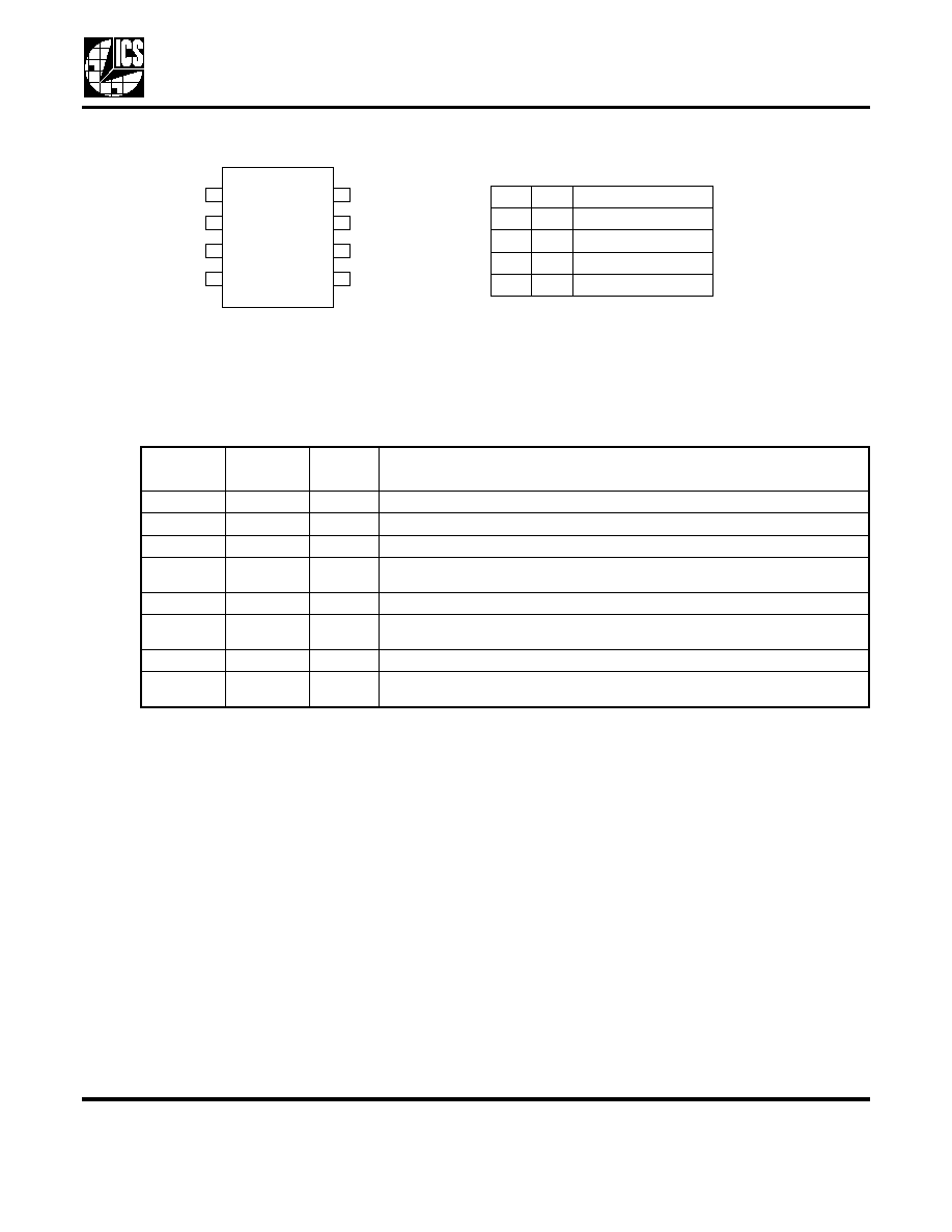
Block Diagram
Divider and
Selection
Circuitry
/32, /64
/256, /512,
CLK1
OE
GND
VDD
X1/ICLK
X2
16.777216
MHz clock
or crystal
input
Optional tuning
capacitors
S1, S0 (1:0)
Clock Divider
MDS 544M-01 A
2
Revision 041505
Integrated Circuit Systems, Inc.
525 Race Street, San Jose, CA 95126
tel (408) 297-1201
www.icst.com
ICS544-01
P R E L I M I N A R Y I N F O R M A T I O N
Pin Assignment
8-pin (150 mil) SOIC
Clock Divider Table
0 = connect directly to ground
1 = connect directly to VDD
Pin Descriptions
External Components
Series Termination Resistor
Clock output traces over one inch should use series
termination. To series terminate a 50
trace (a
commonly used trace impedance), place a 33
resistor
in series with the clock line, as close to the clock output
pin as possible. The nominal impedance of the clock
output is 20
.
On chip capacitors- Crystal capacitors should be
connected from pins X1 to ground and X2 to ground to
optimize the initial accuracy. The value (in pf) of these
crystal caps equal (C
L
-12)*2 in this equation,
C
L
=crystal load capacitance in pf. For example, for a
crystal with a 16 pF load cap, each external crystal cap
would be 8 pF. [(16-12)x2]=8.
Decoupling Capacitor
As with any high-performance mixed-signal IC, the
ICS544-01 must be isolated from system power supply
noise to perform optimally.
A decoupling capacitor of 0.01µF must be connected
between VDD and the PCB ground plane.
PCB Layout Recommendations
For optimum device performance and lowest output
phase noise, the following guidelines should be
observed.
1) The 0.01µF decoupling capacitor should be mounted
on the component side of the board as close to the
X1/ICLK
X2
GND
VDD
S0
OE
CLK
S1
1
2
3
4
8
7
6
5
S1 S0
CLK
0
0
Input/32
0
1
Input/64
1
0
Input/256
1
1
Input/512
Pin
Number
Pin
Name
Pin
Type
Pin Description
1
X1/ICLK
XI
Crystal or Clock input.
2
X2
Xo
Connect to crystal for crystal input and leave open for clock input.
3
GND
Power
Connect to ground.
4
S0
Input
Select 0 for output clock. Connect to GND or VDD, per divider table above.
Internal pull-up resistor.
5
CLK
Output
Clock output per table above.
6
OE
Input
Output Enable.Tri-states output clock when low. Also shuts down the oscillator
circuit. Internal pull-up resistor. OE=1 normal operation.
7
VDD
Power
Connect to 2.25 V to 3.6 V.
8
S1
Input
Select 1 for output clock. Connect to GND or VDD, per divider table above.
Internal pull-up resistor.

Clock Divider
MDS 544M-01 A
3
Revision 041505
Integrated Circuit Systems, Inc.
525 Race Street, San Jose, CA 95126
tel (408) 297-1201
www.icst.com
ICS544-01
P R E L I M I N A R Y I N F O R M A T I O N
VDD pin as possible. No vias should be used between
decoupling capacitor and VDD pin. The PCB trace to
VDD pin should be kept as short as possible, as should
the PCB trace to the ground via. Distance of the ferrite
bead and bulk decoupling from the device is less
critical.
2) To minimize EMI, the 33
series termination resistor
(if needed) should be placed close to the clock output.
3) An optimum layout is one with all components on the
same side of the board, minimizing vias through other
signal layers (the ferrite bead and bulk decoupling
capacitor can be mounted on the back). Other signal
traces should be routed away from the ICS544-01. This
includes signal traces just underneath the device, or on
layers adjacent to the ground plane layer used by the
device.
Absolute Maximum Ratings
Stresses above the ratings listed below can cause permanent damage to the ICS544-01. These ratings,
which are standard values for ICS commercially rated parts, are stress ratings only. Functional operation of
the device at these or any other conditions above those indicated in the operational sections of the
specifications is not implied. Exposure to absolute maximum rating conditions for extended periods can
affect product reliability. Electrical parameters are guaranteed only over the recommended operating
temperature range.
Recommended Operation Conditions
Item
Rating
Supply Voltage, VDD
7 V
All Inputs and Outputs
-0.5 V to VDD+0.5 V
Ambient Operating Temperature
0 to +70
∞C
Storage Temperature
-65 to +150
∞C
Junction Temperature
125
∞C
Soldering Temperature
260
∞C
Parameter
Min.
Typ.
Max.
Units
Ambient Operating Temperature
-40
+85
∞C
Power Supply Voltage (measured in respect to GND)
2.25
3.6
V
Clock Divider
MDS 544M-01 A
4
Revision 041505
Integrated Circuit Systems, Inc.
525 Race Street, San Jose, CA 95126
tel (408) 297-1201
www.icst.com
ICS544-01
P R E L I M I N A R Y I N F O R M A T I O N
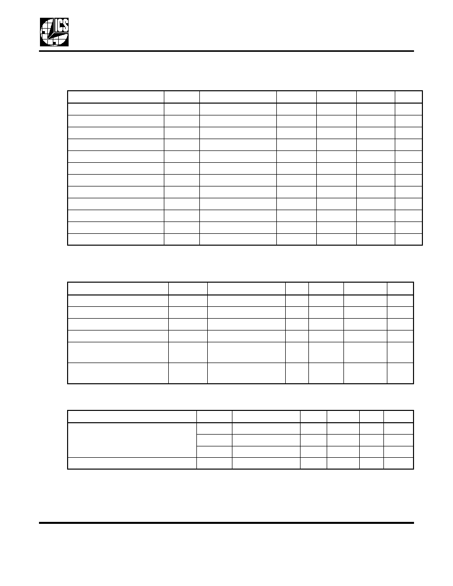
DC Electrical Characteristics
Unless stated otherwise, VDD = 2.25 V to 3.6 V, C
L
=15 pf±5%, Ambient Temperature -40
∞C to +70∞C
AC Electrical Characteristics
Unless stated otherwise, VDD = 2.25 V to 3.6 V±5%, C
L
=15 pf±5%, Ambient Temperature -40
∞C to +70∞C
Thermal Characteristics
Parameter
Symbol
Conditions
Min.
Typ.
Max.
Units
Operating Voltage
VDD
2.25
3.6
V
Input High Voltage
V
IH
S0, S1, OE, ICLK
0.7VDD
V
Input Low Voltage
V
IL
S0, S1, OE, ICLK
0.3VDD
V
Output High Voltage
V
OH
I
OH
= -2 mA
VDD-0.4
VDD-0.15
V
Output Low Voltage
V
OL
I
OL
= 2 mA
0.15
0.4
V
Operating Supply Current
I
DD
VDD =2.25 V - 2.75 V
0.3
0.6
mA
Operating Supply Current
I
DD
VDD= 2.75 V - 3.6 V
0.5
1
mA
Standby Current
I
SB
OE=0 10
ua
Short Circuit Current
I
OS
±40
mA
Input Capacitance
C
IN
S0, S1, OE
4
pF
Nominal Output Impedance
Z
O
at VDD/2
20
Internal Pull-up Resistor
Rpup
TBD
k
Parameter
Symbol
Conditions
Min.
Typ.
Max.
Units
Input Frequency, clock input
VDD = 3.3 V
0
156
MHz
Output Rise Time
t
OR
0.1VDD to 0.9VDD
0.2
1
us
Output Fall Time
t
OF
0.9VDD to 0.1VDD
0.2
1
us
Duty Cycle
at VDD/2
45
49 to 51
55
%
Output Enable Delay Time
t
OE
OE going high to CLK
output valid
2
us
Output Disable Delay Time
t
OD
OE going low to CLK
output invalid
2
us
Parameter
Symbol
Conditions
Min.
Typ.
Max.
Units
Thermal Resistance Junction to
Ambient
JA
Still air
150
∞C/W
JA
1 m/s air flow
140
∞C/W
JA
3 m/s air flow
120
∞C/W
Thermal Resistance Junction to Case
JC
40
∞C/W
Clock Divider
MDS 544M-01 A
5
Revision 041505
Integrated Circuit Systems, Inc.
525 Race Street, San Jose, CA 95126
tel (408) 297-1201
www.icst.com
ICS544-01
P R E L I M I N A R Y I N F O R M A T I O N
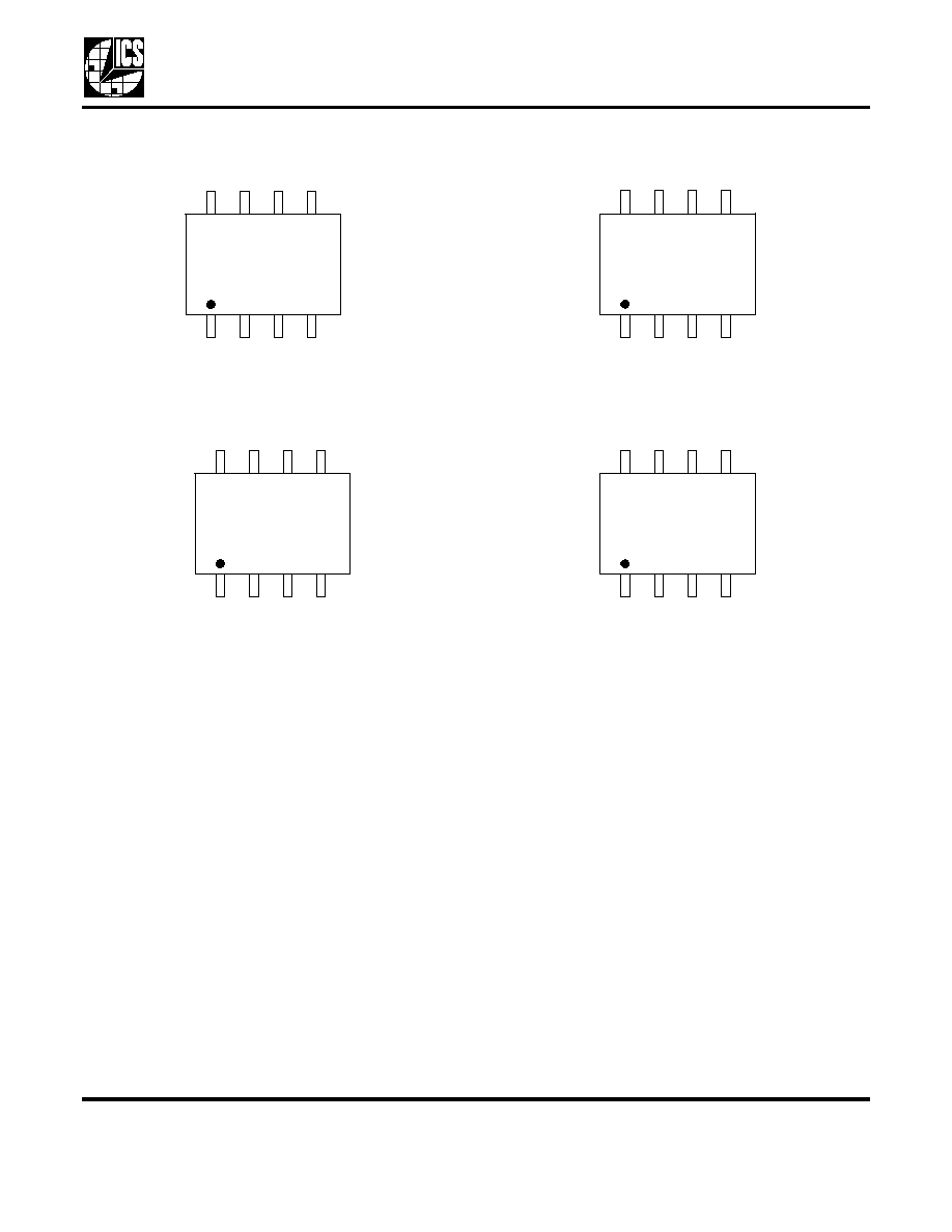
Marking Diagram
(ICS554M-01)
Marking Diagram
(ICS554MI-01)
Marking Diagram
(ICS554M-01LF)
Marking Diagram
(ICS554MI-01LF)
Notes:
1. ###### is the lot number.
2. YYWW is the last two digits of the year and week that the part was assembled.
3. "LF" denotes Pb (lead) free package.
4. "I" denotes industrial temperature range.
5. Bottom Marking: (origin)
Origin = country of origin if not USA.
554M-01
######
YYWW
1
4
5
8
554MI-01
######
YYWW
1
4
5
8
554M01LF
######
YYWW
1
4
5
8
554MI01L
######
YYWW
1
4
5
8
Clock Divider
MDS 544M-01 A
6
Revision 041505
Integrated Circuit Systems, Inc.
525 Race Street, San Jose, CA 95126
tel (408) 297-1201
www.icst.com
ICS544-01
P R E L I M I N A R Y I N F O R M A T I O N
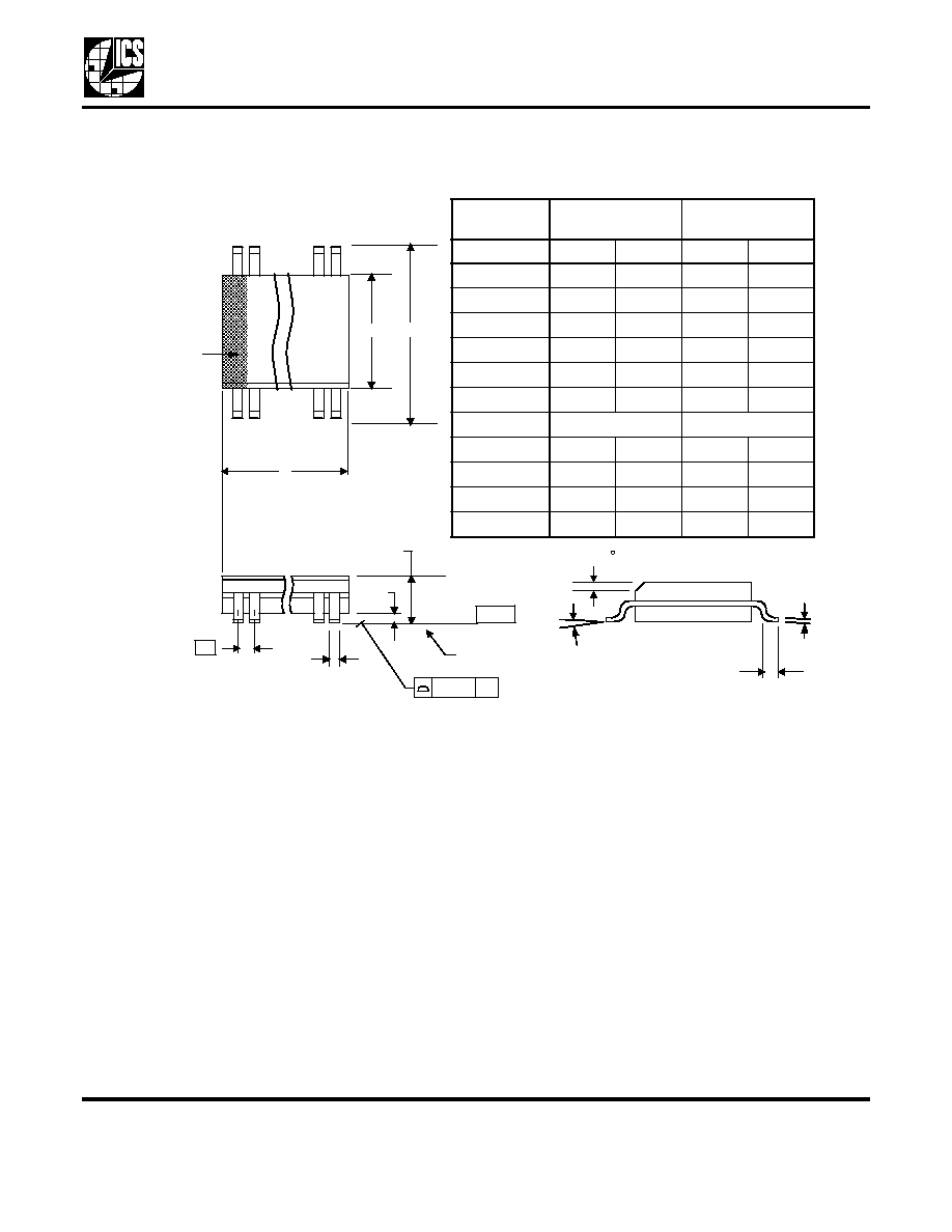
Package Outline and Package Dimensions (8-pin SOIC, 150 Mil. Body)
Package dimensions are kept current with JEDEC Publication No. 95
INDEX
AREA
1 2
8
D
E
SEATING
PLANE
A1
A
e
- C -
B
.10 (.004)
C
C
L
H
h x 45
Millimeters
Inches
Symbol
Min
Max
Min
Max
A
1.35
1.75
.0532
.0688
A1
0.10
0.25
.0040
.0098
B
0.33
0.51
.013
.020
C
0.19
0.25
.0075
.0098
D
4.80
5.00
.1890
.1968
E
3.80
4.00
.1497
.1574
e
1.27 BASIC
0.050 BASIC
H
5.80
6.20
.2284
.2440
h
0.25
0.50
.010
.020
L
0.40
1.27
.016
.050
0
∞
8
∞
0
∞
8
∞
Clock Divider
MDS 544M-01 A
7
Revision 041505
Integrated Circuit Systems, Inc.
525 Race Street, San Jose, CA 95126
tel (408) 297-1201
www.icst.com
ICS544-01
P R E L I M I N A R Y I N F O R M A T I O N
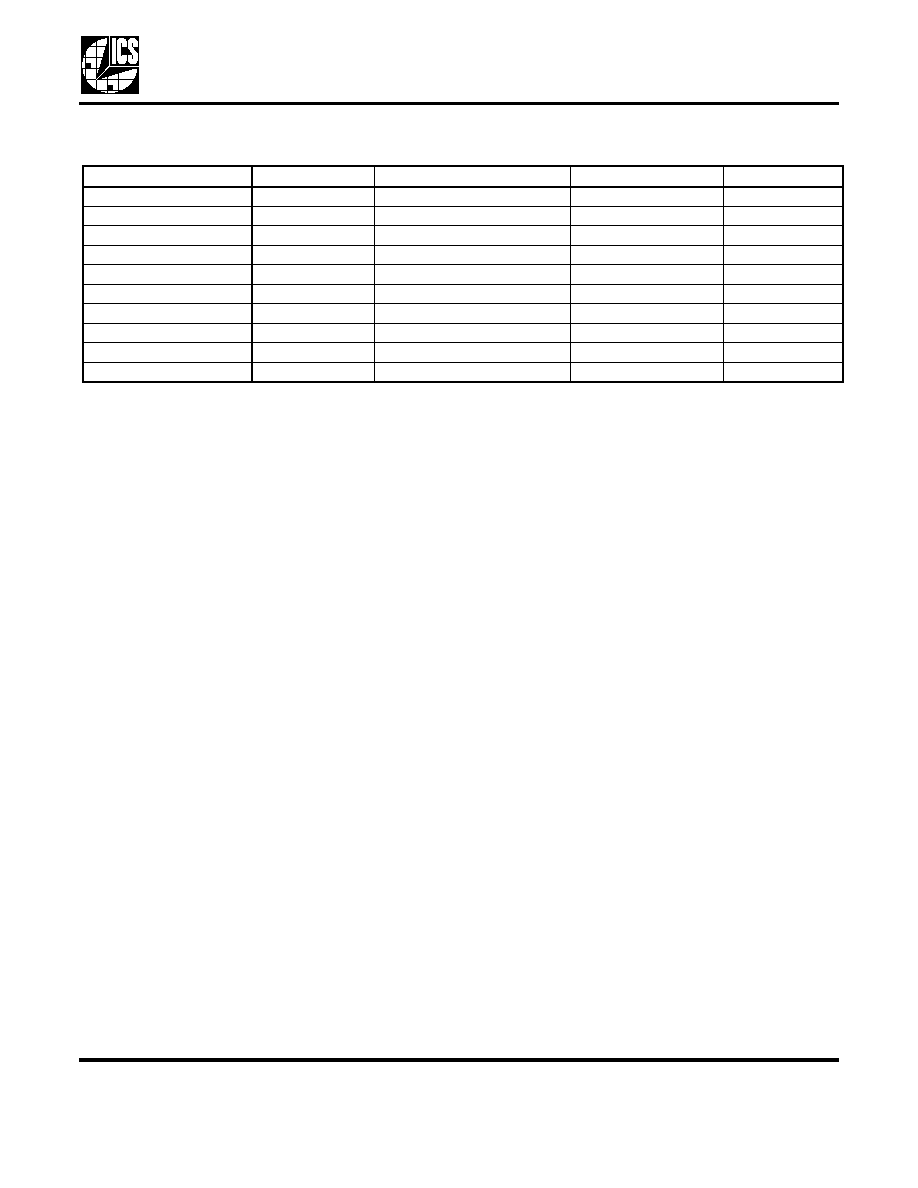
Ordering Information
Parts that are ordered with a "LF" suffix to the part number are the Pb-Free configuration and are RoHS compliant.
While the information presented herein has been checked for both accuracy and reliability, Integrated Circuit Systems (ICS)
assumes no responsibility for either its use or for the infringement of any patents or other rights of third parties, which would
result from its use. No other circuits, patents, or licenses are implied. This product is intended for use in normal commercial
applications. Any other applications such as those requiring extended temperature range, high reliability, or other extraordinary
environmental requirements are not recommended without additional processing by ICS. ICS reserves the right to change any
circuitry or specifications without notice. ICS does not authorize or warrant any ICS product for use in life support devices or
critical medical instruments.
Part / Order Number
Marking
Shipping Packaging
Package
Temperature
ICS544M-01
544M-01
Tubes
8-pin SOIC
0 to +70
∞ C
ICS544M-01T
544M-01
Tape and Reel
8-pin SOIC
0 to +70
∞ C
ICS544MI-01
544MI-01
Tubes
8-pin SOIC
-40 to +85
∞ C
ICS544MI-01T
544MI-01
Tape and Reel
8-pin SOIC
-40 to +85
∞ C
ICS544M-01LF
544M01LF
Tubes
8-pin SOIC
0 to +70
∞ C
ICS544M-01LFT
544M01LF
Tape and Reel
8-pin SOIC
0 to +70
∞ C
ICS544MI-01LF
544MI01L
Tubes
8-pin SOIC
-40 to +85
∞ C
ICS544MI-01LFT
544MI01L
Tape and Reel
8-pin SOIC
-40 to +85
∞ C
ICS554-01DWF
Die on uncut, probed wafers
0 to +70
∞ C
ICS554-01DPK
Tested die in waffle pack
0 to +70
∞ C