 | –≠–ª–µ–∫—Ç—Ä–æ–Ω–Ω—ã–π –∫–æ–º–ø–æ–Ω–µ–Ω—Ç: 650-14B | –°–∫–∞—á–∞—Ç—å:  PDF PDF  ZIP ZIP |
ICS650-14B
Networking System Clock
MDS 650-14B B
1
Revision 072401
Integrated Circuit Systems, Inc. ∑ 525 Race Street ∑ San Jose ∑ CA ∑ 95126 ∑ (408)295-9800te l ∑ www.icst.com
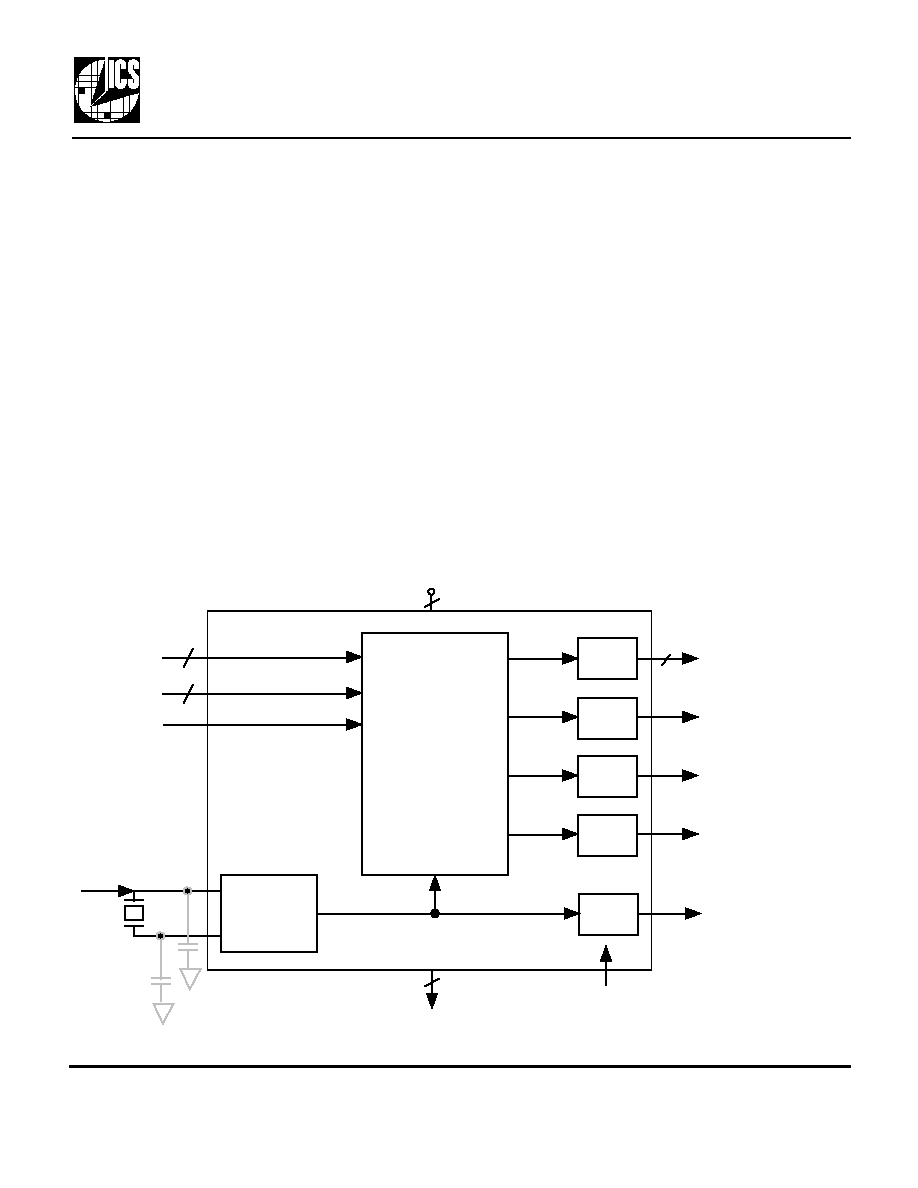
The ICS650-14B is a low cost, low jitter, high
performance clock synthesizer customized for
networking systems applications. Using analog Phase-
Locked Loop (PLL) techniques, the device accepts a
25.0 MHz clock or fundamental mode crystal input to
produce multiple output clocks of one fixed 25.0 MHz,
a four (plus one) frequency selectable bank, and two
frequency selectable clocks. All output clocks are
frequency locked together. The ICS650R-14B
outputs all have 0 ppm synthesis error.
Block Diagram
Description
Features
∑ Packaged in 20 pin (150 mil) SSOP (QSOP)
∑ 25.00 MHz fundamental crystal or clock input
∑ One fixed output clock of one 25.0 MHz
∑ One bank of four frequency selectable
output clocks
∑ Three frequency selectable clock outputs
∑ Zero ppm synthesis error in all clocks
∑ Ideal for networking systems
∑ Full CMOS output swing
∑ Advanced, low power, sub-micron CMOS process
∑ 3.0V to 5.5V operating voltage
∑ Industrial temperature range available
Clock
Buffer/
Crystal
Oscillator
VDD
GND
Clock Synthesis
and Control Circuitry
25.00 MHz
crystal or clock
25.00 MHz
2
2
Output
Buffer
CLKA5
Output
Buffer
X1/ICLK
X2
CLKB
Output
Buffer
Optional crystal capacitors are shown and may be required for tuning of initial accuracy (determined once per
board).
OE (All outputs)
Output
Buffer
CLKA 1:4
4
SELA 0:1
2
SELB 0:1
2
SELC
CLKC
Output
Buffer
ICS650-14B
Networking System Clock
MDS 650-14B B
2
Revision 072401
Integrated Circuit Systems, Inc. ∑ 525 Race Street ∑ San Jose ∑ CA ∑ 95126 ∑ (408)295-9800te l ∑ www.icst.com
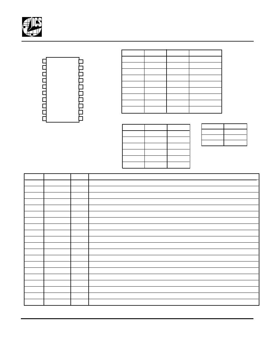
Pin Descriptions
Key: XI, XO = crystal connections; I = Input; I(Pu) = Input with pull up O = Output; P = power supply connection; TI = tri
level input
Number
Name
Type
Description
1
SELB0
TI
Select pin for CLKB. See Table 2.
2
X2
XO
Crystal connection. Connect to 25 MHz crystal or leave unconnected for a clock input.
3
X1/ICLK
XI
Crystal connection. Connect to 25 MHz fundamental crystal or clock input.
4
VDD
P
Connect to +3.3 V or +5 V. Must be same as other VDDs.
5
SELB1
I(Pu)
Select pin for CLK B. See table 2.
6
GND
P
Connect to ground.
7
CLKB
O
Selectable clock output. See Table 2.
8
CLKC
O
Selectable clock output. See Table 3.
9
CLKA5
O
Selectable clock output. See Table 1.
10
25M
O
25.0 MHz clock output.
11
OE
I(Pu)
Output Enable. Tri-states all output clocks when low. Internal pull-up.
12
CLKA1
O
Selectable clock output. See Table 1.
13
CLKA4
O
Selectable clock output. See Table 1.
14
GND
P
Connect to ground.
15
SELA1
TI
Select pin for CLKA1:4 and CLKA5 outputs. See Table 1.
16
VDD
P
Connect to +3.3V or +5.0V. Must be same as other VDDs.
17
CLKA3
O
Selectable clock output. See Table 1.
18
CLKA2
O
Selectable clock output. See Table 1.
19
SELA0
TI
Select pin for CLKA1:4 and CLKA5 outputs. See Table 1.
20
SELC
TI
Select pin for CLKC output. See Table 3.
Pin Assignment
1
16
2
3
4
15
14
13
VDD
CLKA5
X2
VDD
20 pin (150 mil) SSOP
5
6
7
8
12
11
10
9
25M
SELA0
X1/ICLK
SELB0
CLKA2
SELC
CLKA3
CLKA1
OE
CLKC
CLKB
18
17
19
20
GND
SELB1
CLKA4
GND
SELA1
SELC
CLKC
0
CLKB/4
M
62.5
1
125
Table 3
0 = connect directly to ground
1 = connect directly to VDD
M = leave unconnected
(floating)
SELB1
SELB0
CLKB
0
0
30
0
M
27
0
1
48
1
0
83.33
1
M
19.44
1
1
80
Table 2
SELA1
SELA0
CLKA1:4
CLKA5
0
0
33.33
66.66
0
M
50
75
0
1
66.67
133.33
M
0
100
33.33
M
M
33.33
83.33
M
1
50
125
1
0
33.33
100
1
M
25
75
1
1
66.67
100
Table 1
ICS650-14B
Networking System Clock
MDS 650-14B B
3
Revision 072401
Integrated Circuit Systems, Inc. ∑ 525 Race Street ∑ San Jose ∑ CA ∑ 95126 ∑ (408)295-9800te l ∑ www.icst.com
Parameter
Conditions
Minimum
Typical
Maximum
Units
ABSOLUTE MAXIMUM RATINGS (note 1)
ABSOLUTE MAXIMUM RATINGS (note 1)
Supply voltage, VDD
Referenced to GND
7
V
Inputs and Clock Outputs
Referenced to GND
-0.5
VDD+0.5
V
Ambient Operating Temperature
0
70
∞C
Ambient Operating Temperature
Industrial "I" version
-40
85
∞C
Soldering Temperature
Max of 20 seconds
260
∞C
Storage temperature
-65
150
∞C
DC CHARACTERISTICS (VDD = 3.3V unless noted)
DC CHARACTERISTICS (VDD = 3.3V unless noted)
Operating Voltage, VDD
3
5.5
V
Input High Voltage, VIH, X1 pin only
Clock Input
VDD/2 + 1
V
Input Low Voltage, VIL, X1 pin only
Clock Input
VDD/2 - 1
V
Input High Voltage, VIH, SEL pins only
VDD - 0.5
V
Input Low Voltage, VIL, SEL pins only
0.5
V
Input High Voltage, VIH, OE pin only
2.0
V
Input Low Voltage, VIL, OE pin only
0.8
V
Output High Voltage, VOH
IOH=-12mA
2.4
V
Output Low Voltage, VOL
IOL=12mA
0.4
V
Output High Voltage, VOH, CMOS level
IOH=-8mA
VDD-0.4
V
Operating Supply Current, IDD
No Load, VDD = 3.3V
32
mA
Short Circuit Current
Each output
±50
mA
AC CHARACTERISTICS (VDD = 3.3V unless noted)
AC CHARACTERISTICS (VDD = 3.3V unless noted)
Input Frequency
25.000
MHz
Output Clock Rise Time
0.8 to 2.0V
1.5
ns
Output Clock Fall Time
2.0 to 0.8V
1.5
ns
Output Clock Duty Cycle
At VDD/2
45
50
55
%
Frequency error
All clocks
0
ppm
Absolute Jitter, short term
CLKB = 27M
±250
ps
CLKC = 6.25M
ps
Other Clocks
±150
ps
Electrical Specifications
Notes: 1. Stresses beyond those listed under Absolute Maximum Ratings could cause permanent damage to the
device. Prolonged exposure to levels above the operating limits but below the Absolute Maximums may
affect device reliability.
2. CMOS level input, nominal trip point is VDD/2 for 3.3 V or 5 V operation.
External Components
The ICS650R-14B requires a minimum number of external components for proper operation. Decoupling capacitors
of 0.01µF should be connected between each VDD and GND on Pins 4 and 6, and Pins 16 and 14, as close to the
ICS650R-14B as possible. A series termination resistor of 33
may be used for each clock output. The 25.00 MHz
crystal must be connected as close to the chip as possible. The crystal should be a fundamental mode (do not use
third overtone), parallel resonant. Crystal capacitors should be connected from pins X1 to ground and X2 to ground
to optimize the initial accuracy. The value of these capacitors is given by the following equation, where CL is the
crystal load capacitance: Crystal caps (pF) = (CL-6) x 2. For a crystal with 16 pF load capacitance, two 20 pF caps
should be used.

ICS650-14B
Networking System Clock
MDS 650-14B B
4
Revision 072401
Integrated Circuit Systems, Inc. ∑ 525 Race Street ∑ San Jose ∑ CA ∑ 95126 ∑ (408)295-9800te l ∑ www.icst.com
While the information presented herein has been checked for both accuracy and reliability, Integrated Circuit Systems, Inc (ICS) assumes no
responsibility for either its use or for the infringement of any patents or other rights of third parties, which would result from its use. No other circuits,
patents, or licenses are implied. This product is intended for use in normal commercial applications. Any other applications such as those requiring
extended temperature range, high reliability, or other extraordinary environmental requirements are not recommended without additional processing by
ICS. ICS reserves the right to change any circuitry or specifications without notice. ICS does not authorize or warrant any ICS product for use in life
support devices or critical medical instruments.
Ordering Information for ICS650-14B
Part/Order Number
Marking
Shipping packaging
Package
Temperature
ICS650R-14
ICS650R-14
tubes
20 pin SSOP
0 to +70 ∞C
ICS650R-14T
ICS650R-14
tape and reel
20 pin SSOP
0 to +70 ∞C
ICS650R-14I
ICS650R-14I
tubes
20 pin SSOP
-40 to +85 ∞C
ICS650R-14IT
ICS650R-14I
tape and reel
20 pin SSOP
-40 to +85 ∞C
Package Outline and Package Dimensions
(For current dimensional specifications, see JEDEC Publication No. 95.)
b
D
E1
E
e
A1
c
A
L
INDEX
AREA
1
2
2 0 p i n S S O P
Inches
Inches
Millimeters
Millimeters
Symbol
Min
Max
Min
Max
A
0.053
0.069
1.35
1.75
A1
0.004
0.010
0.10
0.25
b
0.008
0.012
0.20
0.30
c
0.007
0.010
0.18
0.25
D
0.337
0.344
8.55
8.75
e .025 BSC
.025 BSC 0.635 BSC
0.635 BSC
E
0.228
0.244
5.80
6.20
E1
0.150
0.157
3.80
4.00
L
0.016
0.050
0.40
1.27