ICS7152A
MDS 7152A A
1
Revision 102005
Integrated Circuit Systems, Inc.
525 Race Street, San Jose, CA 95126
tel (408) 297-1201
www.icst.com
Spread Spectrum Clock Generator
Description
The ICS7152A-02 and -11 are clock generators for EMI
(Electromagnetic Interference) reduction (see below for
frequency ranges and multiplier ratios). Spectral peaks
are attenuated by modulating the system clock
frequency. Down or center spread profiles are
selectable. Down spread will not exceed the maximum
frequency of an unspread clock, and center spread
does not change the average operating frequency of
the system
ICS offers many other clocks for computers and
computer peripherals. Consult ICS when you need to
remove crystals and oscillators from your board.
Features
�
Operating voltage of 3.3 V �0.3 V
�
Packaged in 8-pin SOIC
�
Input frequency range of 16.6 to 134.0 MHz
�
Output frequency range of 16.6 to 134.0 MHz
�
Provides a spread spectrum clock output (�0.5%,
�1.5% center spread; -1.0%, -3.0% down spread)
�
Low cycle-to-cycle jitter - less than 100 ps
�
Advanced, low-power CMOS process
�
Industrial and commercial temperature ranges
�
Available in Pb (lead) free package
�
Pin compatible with Fujitsu MB88152-102 and -111
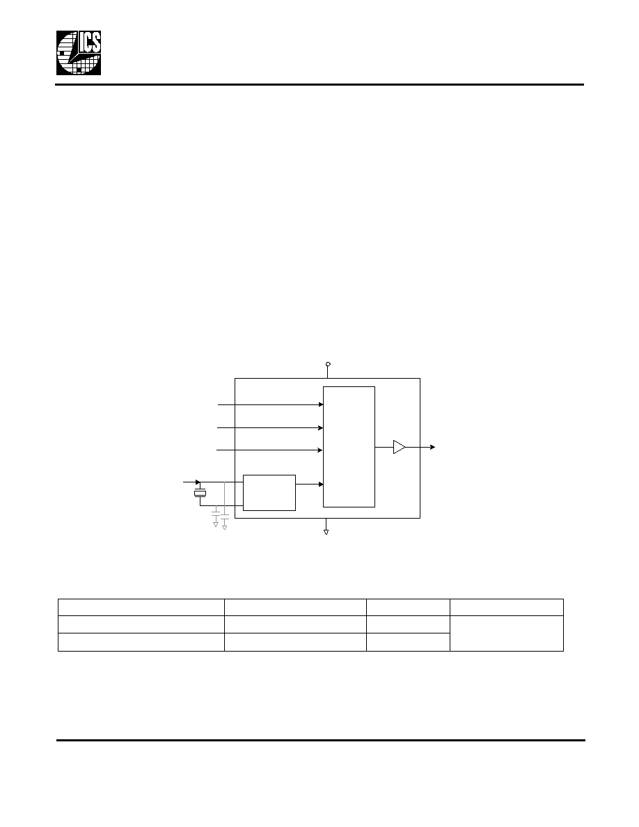
Block Diagram
Product Lineup
Product
Input Frequency Range
Modulation Type
Modulation Enable Pin
ICS7152AM-02, ICS7152AMI-02
40.0 MHz to 134.0 MHz
Down spread
Yes
ICS7152AM-11, ICS7152AMI-11
16.6 MHz to 67.0 MHz
Center spread
PLL Clock
Synthesis
and Spread
Spectrum
Circuitry
SEL
FREQ
CKOUT
GND
VDD
Clock Buffer/
Crystal
Ocsillator
XIN
XOUT
External caps required with crystal for
accurate tuning of the clock
XENS
Spread Spectrum Clock Generator
MDS 7152A A
2
Revision 102005
Integrated Circuit Systems, Inc.
525 Race Street, San Jose, CA 95126
tel (408) 297-1201
www.icst.com
ICS7152A
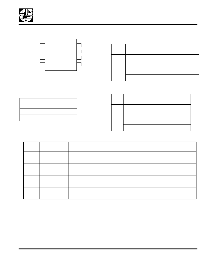
Pin Assignment
Modulation Enable Select Table
Spread Direction and Percentage
Select Table
Frequency Select Table
Pin Descriptions
XENS
Pin 8
Modulation
0
Modulation
1
No modulation
XENS
XOUT
GND
FREQ
SEL
CKOUT
VDD
XIN
1
2
3
4
8
7
6
5
8 pin (150 mil) SOIC
SEL
Pin 4
Spread
Direction
Spread
Percentage (%)
Part Number
0
Center
�0.5
ICS7152AM-11
Down
-1.0
ICS7152AM-02
1
Center
�1.5
ICS7152AM-11
Down
-3.0
ICS7152AM-02
FREQ
Pin 7
Frequency
0
16.6 to 40 MHz
ICS7152AM-11
40 to 80 MHz
ICS7152AM-02
1
33 to 67 MHz
ICS7152AM-11
66 to 134 MHz
ICS7152AM-02
Pin
Number
Pin
Name
Pin Type
Pin Description
1
XIN
Input
Crystal/clock input pin.
2
XOUT
Output
Crystal.
3
GND
Power
Connect to ground.
4
SEL
Input
Spread modulation select.
5
CKOUT
Output
Spread modulation select.
6
VDD
Power
Connect to +3.3 V.
7
FREQ
Input
Frequency select.
8
XENS
Output
Modulation enable select.

Spread Spectrum Clock Generator
MDS 7152A A
3
Revision 102005
Integrated Circuit Systems, Inc.
525 Race Street, San Jose, CA 95126
tel (408) 297-1201
www.icst.com
ICS7152A
External Components
The ICS7152A requires a minimum number of external
components for proper operation.
Decoupling Capacitor
A decoupling capacitor of 0.01�F must be connected
between GND and VDD on pins 3 and 6, as close to
these pins as possible. For optimum device
performance, the decoupling capacitor should be
mounted on the component side of the PCB. Avoid the
use of vias in the decoupling circuit.
Series Termination Resistor
Series termination should be used on the clock output.
To series terminate a 50
trace (a commonly used
trace impedance) place a 27
resistor in series with
the clock line, as close to the clock output pin as
possible. The nominal impedance of the clock output is
25
.
PCB Layout Recommendations
For optimum device performance and lowest output
phase noise, the following guidelines should be
observed.
1) The 0.01�F decoupling capacitor should be mounted
on the component side of the board as close to the
VDD pin as possible. No vias should be used between
the decoupling capacitor and VDD pin. The PCB trace
to VDD pin should be kept as short as possible, as
should the PCB trace to the ground via.
2) To minimize EMI, the 27
series termination resistor
(if needed) should be placed close to the clock output.
3) An optimum layout is one with all components on the
same side of the board, minimizing vias through other
signal layers. Other signal traces should be routed
away from the ICS7152A. This includes signal traces
just underneath the device, or on layers adjacent to the
ground plane layer used by the device.
Crystal Information
The crystal used should be a fundamental mode,
parallel resonant. Crystal capacitors should be
connected from pins X1 to ground and X2 to ground to
optimize the initial accuracy. The value of these
capacitors is given by the following equation:
Crystal caps (pF) = (C
L
- 6) x 2
In the equation, C
L
is the crystal load capacitance. So,
for a crystal with a 16 pF load capacitance, two 20 pF
[(16-6) x 2] capacitors should be used.
Spread Spectrum Profile
The ICS7152A low EMI clock generator uses a
triangular frequency modulation profile for optimal
down stream tracking of zero delay buffers and other
PLL devices. The frequency modulation amplitude is
constant with variations of the input frequency.
Time
F
r
eq
ue
nc
y
Modulation Rate

Spread Spectrum Clock Generator
MDS 7152A A
4
Revision 102005
Integrated Circuit Systems, Inc.
525 Race Street, San Jose, CA 95126
tel (408) 297-1201
www.icst.com
ICS7152A
Absolute Maximum Ratings
Stresses above the ratings listed below can cause permanent damage to the ICS7152A. These ratings,
which are standard values for ICS commercially rated parts, are stress ratings only. Functional operation of
the device at these or any other conditions above those indicated in the operational sections of the
specifications is not implied. Exposure to absolute maximum rating conditions for extended periods can
affect product reliability. Electrical parameters are guaranteed only over the recommended operating
temperature range.
Overshoot/Undershoot
Recommended Operation Conditions
Item
Rating
Supply Voltage, VDD
-0.5 to 4.0 V
All Inputs and Outputs (referenced to GND)
-0.5 V to VDD+0.5 V
Ambient Operating Temperature
-40 to +85
�C
Storage Temperature
-55 to +125
�C
Junction Temperature
-40 to +125
�C
Soldering Temperature
260
�C
Overshoot (V
IOVER
)
VDD + 1.0 V (t
OVER
< 50 ns) max
Undershoot (V
IUNDER
)
GND - 1.0 V (t
UNDER
< 50 ns) min
Parameter
Min.
Typ.
Max.
Units
Ambient Operating Temperature
-40
+85
�C
Power Supply Voltage (measured in respect to GND)
+3.0
3.3
3.6
V
Input pin
V
IOVER
< V
DD
+ 1.0 V
V
IUNDER
< GND - 1.0 V
t
OVER
< 50 ns
t
UNDER
< 50 ns
V
DD
GND

Spread Spectrum Clock Generator
MDS 7152A A
5
Revision 102005
Integrated Circuit Systems, Inc.
525 Race Street, San Jose, CA 95126
tel (408) 297-1201
www.icst.com
ICS7152A
DC Electrical Characteristics
Unless stated otherwise, VDD = 3.3 V �0.3 V, Ambient Temperature -40 to +85
�C
Parameter
Symbol
Conditions
Min.
Typ.
Max.
Units
Operating Voltage
VDD
3.0
3.3
3.6
V
Supply Current
IDD
No load, at 3.3 V,
output = 24 MHz
10
14
mA
Input High Voltage
V
IH
SEL, FREQ, XENS
VDD x 0.8
VDD + 0.3
V
XIN, Input slew rate
3 V/ns, 16.6 to 100
MHz
VDD x 0.8
VDD + 0.3
V
XIN, Input slew rate
3 V/ns, 100 to 134
MHz
VDD x 0.9
VDD + 0.3
V
Input Low Voltage
V
IL
SEL, FREQ, XENS
GND
VDD x 0.20
V
XIN, Input slew rate
3 V/ns, 16.6 to 100
MHz
GND
VDD x 0.20
V
XIN, Input slew rate
3 V/ns, 100 to 134
MHz
GND
VDD x 0.10
V
Output High Voltage
V
OH
CKOUT, I
OH
= -4 mA
VDD - 0.5
VDD
V
Output Low Voltage
V
OL
CKOUT, I
OL
= 4 mA
GND
0.4
V
Input Capacitance
C
IN
XIN, SEL, XENS
16
pF
Load Capacitance
C
L
CKOUT, 16.6 to 67
MHz
15
pF
CKOUT, 67 to 100
MHz
10
pF
CKOUT, 100 to 134
MHz
7
pF
Output Impedance
Z
O
CKOUT, 16.6 to 134
MHz
25