Document Outline
- FEATURES
- APPLICATIONS
- DESCRIPTION
- QUICK REFERENCE DATA
- FUNCTION TABLE
- ORDERING INFORMATION
- PINNING
- RECOMMENDED OPERATING CONDITIONS
- LIMITING VALUES
- DC CHARACTERISTICS
- TRANSFER CHARACTERISTICS
- AC CHARACTERISTICS
- AC WAVEFORMS
- PACKAGE OUTLINES
- DATA SHEET STATUS
- DEFINITIONS
- DISCLAIMERS

DATA SHEET
Product specification
2003 Aug 13
INTEGRATED CIRCUITS
74LVC2G17
Dual non-inverting Schmitt-trigger
with 5 V tolerant input

2003 Aug 13
2
Philips Semiconductors
Product specification
Dual non-inverting Schmitt-trigger with
5 V tolerant input
74LVC2G17
FEATURES
∑
Wide supply voltage range from 1.65 to 5.5 V
∑
5 V tolerant input/output for interfacing with 5 V logic
∑
High noise immunity
∑
Complies with JEDEC standard:
≠ JESD8-7 (1.65 to 1.95 V)
≠ JESD8-5 (2.3 to 2.7 V)
≠ JESD8B/JESD36 (2.7 to 3.6 V).
∑
ESD protection:
≠ HBM EIA/JESD22-A114-A exceeds 2000 V
≠ MM EIA/JESD22-A115-A exceeds 200 V.
∑ ±
24 mA output drive (V
CC
= 3.0 V)
∑
CMOS low power consumption
∑
Latch-up performance exceeds 250 mA
∑
Direct interface with TTL levels
∑
SOT363 and SOT457 package
∑
Specified from
-
40 to +125
∞
C.
APPLICATIONS
∑
Wave and pulse shapers for highly noisy environments.
DESCRIPTION
The 74LVC2G17 is a high-performance, low-power,
low-voltage, Si-gate CMOS device and superior to most
advanced CMOS compatible TTL families.
Inputs can be driven from either 3.3 or 5 V devices. These
feature allows the use of these devices as translators in a
mixed 3.3 and 5 V environment.
This device is fully specified for partial power-down
applications using I
off
. The I
off
circuitry disables the output,
preventing the damaging back flow current through the
device when it is powered down.
The 74LVC2G17 provides two non-inverting buffers with
Schmitt-trigger action. It is capable of transforming slowly
changing input signals into sharply defined, jitter-free
output signals.
QUICK REFERENCE DATA
GND = 0 V; T
amb
= 25
∞
C.
Notes
1. C
PD
is used to determine the dynamic power dissipation (P
D
in
µ
W).
P
D
= C
PD
◊
V
CC
2
◊
f
i
◊
N +
(C
L
◊
V
CC
2
◊
f
o
) where:
f
i
= input frequency in MHz;
f
o
= output frequency in MHz;
C
L
= output load capacitance in pF;
V
CC
= supply voltage in Volts;
N = total load switching outputs;
(C
L
◊
V
CC
2
◊
f
o
) = sum of outputs.
2. The condition is V
I
= GND to V
CC
.
SYMBOL
PARAMETER
CONDITIONS
TYPICAL
UNIT
t
PHL
/t
PLH
propagation delay inputs nA to output nY V
CC
= 1.8 V; C
L
= 30 pF; R
L
= 1 k
5.6
ns
V
CC
= 2.5 V; C
L
= 30 pF; R
L
= 500
3.7
ns
V
CC
= 2.7 V; C
L
= 50 pF; R
L
= 500
3.8
ns
V
CC
= 3.3 V; C
L
= 50 pF; R
L
= 500
3.6
ns
V
CC
= 5.0 V; C
L
= 50 pF; R
L
= 500
2.7
ns
C
I
input capacitance
3.5
pF
C
PD
power dissipation capacitance per buffer
V
CC
= 3.3 V; notes 1 and 2
16.3
pF
2003 Aug 13
3
Philips Semiconductors
Product specification
Dual non-inverting Schmitt-trigger with
5 V tolerant input
74LVC2G17
FUNCTION TABLE
See note 1.
Note
1. H = HIGH voltage level;
L = LOW voltage level.
ORDERING INFORMATION
PINNING
INPUT
OUTPUT
nA
nY
L
L
H
H
TYPE NUMBER
PACKAGES
TEMPERATURE
RANGE
PINS
PACKAGE
MATERIAL
CODE
MARKING
74LVC2G17GW
-
40 to +125
∞
C
6
SC-88
plastic
SOT363
VV
74LVC2G17GV
-
40 to +125
∞
C
6
SC-74
plastic
SOT457
V17
PIN
SYMBOL
DESCRIPTION
1
1A
data input
2
GND
ground (0 V)
3
2A
data input
4
2Y
data output
5
V
CC
supply voltage
6
1Y
data output
2003 Aug 13
4
Philips Semiconductors
Product specification
Dual non-inverting Schmitt-trigger with
5 V tolerant input
74LVC2G17
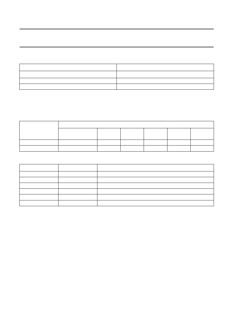
Fig.1 Pin configuration.
handbook, halfpage
1
2
5
3
6
4
MNB065
17
VCC
GND
2Y
1Y
2A
1A
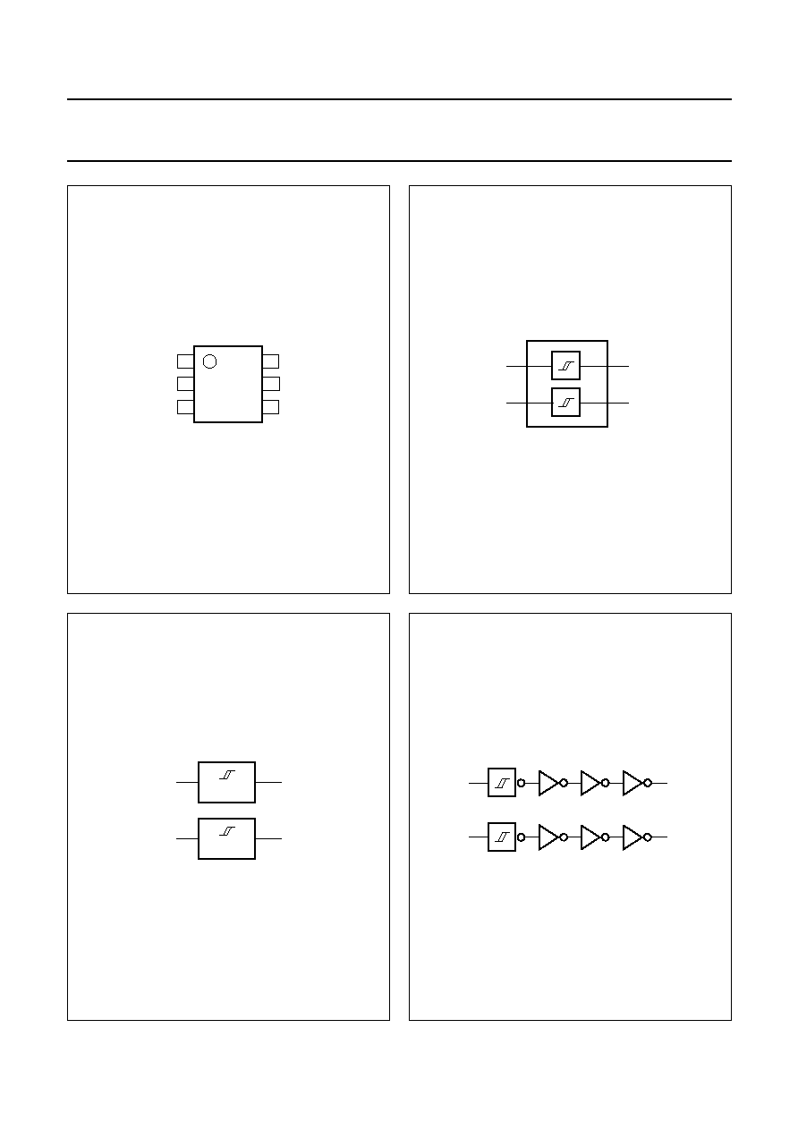
handbook, halfpage
MNB066
1A
1Y
1
6
2A
2Y
3
4
Fig.2 Logic symbol.
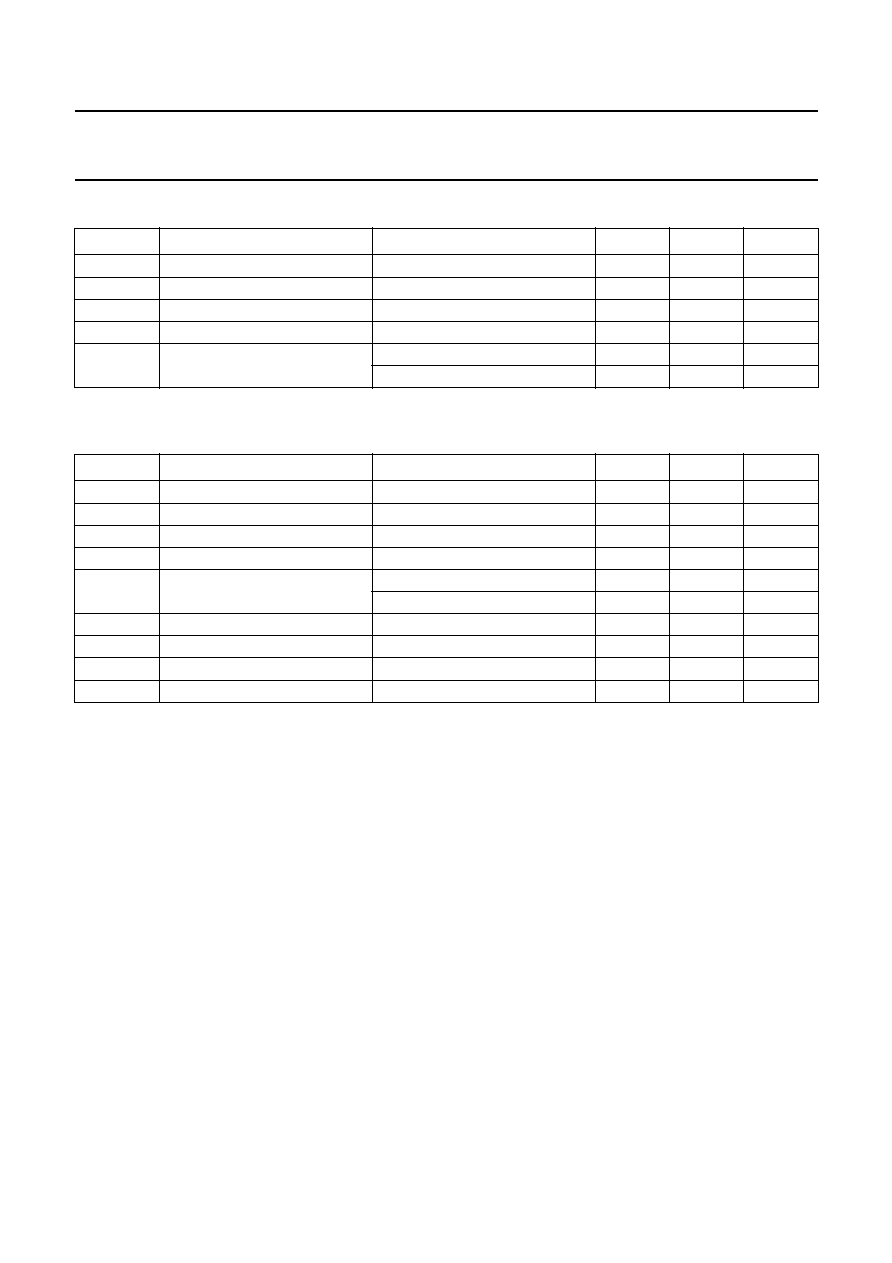
handbook, halfpage
6
1
4
3
MNB067
Fig.3 IEC logic symbol.
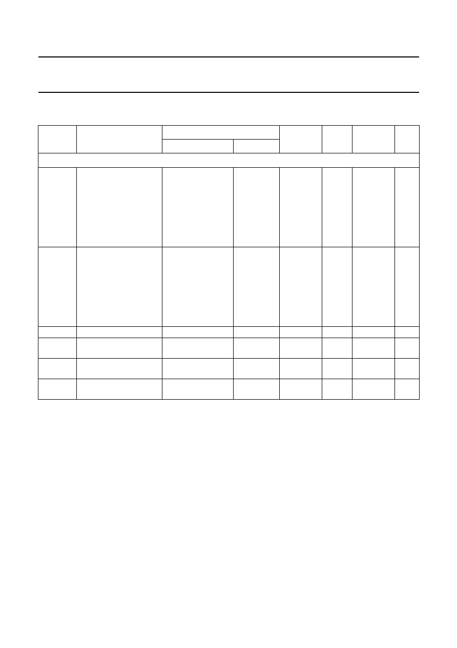
handbook, halfpage
MNB068
1A
1Y
2A
2Y
Fig.4 Logic diagram.
2003 Aug 13
5
Philips Semiconductors
Product specification
Dual non-inverting Schmitt-trigger with
5 V tolerant input
74LVC2G17
RECOMMENDED OPERATING CONDITIONS
LIMITING VALUES
In accordance with the Absolute Maximum Rating System (IEC 60134); voltages are referenced to GND (ground = 0 V).
Notes
1. The input and output voltage ratings may be exceeded if the input and output current ratings are observed.
2. When V
CC
= 0 V (Power-down mode), the output voltage can be 5.5 V in normal operation.
SYMBOL
PARAMETER
CONDITIONS
MIN.
MAX.
UNIT
V
CC
supply voltage
1.65
5.5
V
V
I
input voltage
0
5.5
V
V
O
output voltage
0
V
CC
V
T
amb
operating ambient temperature
-
40
+125
∞
C
t
r
, t
f
input rise and fall times
V
CC
= 1.65 to 2.7 V
0
20
ns/V
V
CC
= 2.7 to 5.5 V
0
10
ns/V
SYMBOL
PARAMETER
CONDITIONS
MIN.
MAX.
UNIT
V
CC
supply voltage
-
0.5
+6.5
V
I
IK
input diode current
V
I
< 0
-
-
50
mA
V
I
input voltage
note 1
-
0.5
+6.5
V
I
OK
output diode current
V
O
> V
CC
or V
O
< 0
-
±
50
mA
V
O
output voltage
active mode; notes 1 and 2
-
0.5
V
CC
+ 0.5
V
Power-down mode; notes 1 and 2
-
0.5
+6.5
V
I
O
output source or sink current
V
O
= 0 to V
CC
-
±
50
mA
I
CC
, I
GND
V
CC
or GND current
-
±
100
mA
T
stg
storage temperature
-
65
+150
∞
C
P
D
power dissipation
T
amb
=
-
40 to +125
∞
C
-
300
mW
2003 Aug 13
6
Philips Semiconductors
Product specification
Dual non-inverting Schmitt-trigger with
5 V tolerant input
74LVC2G17
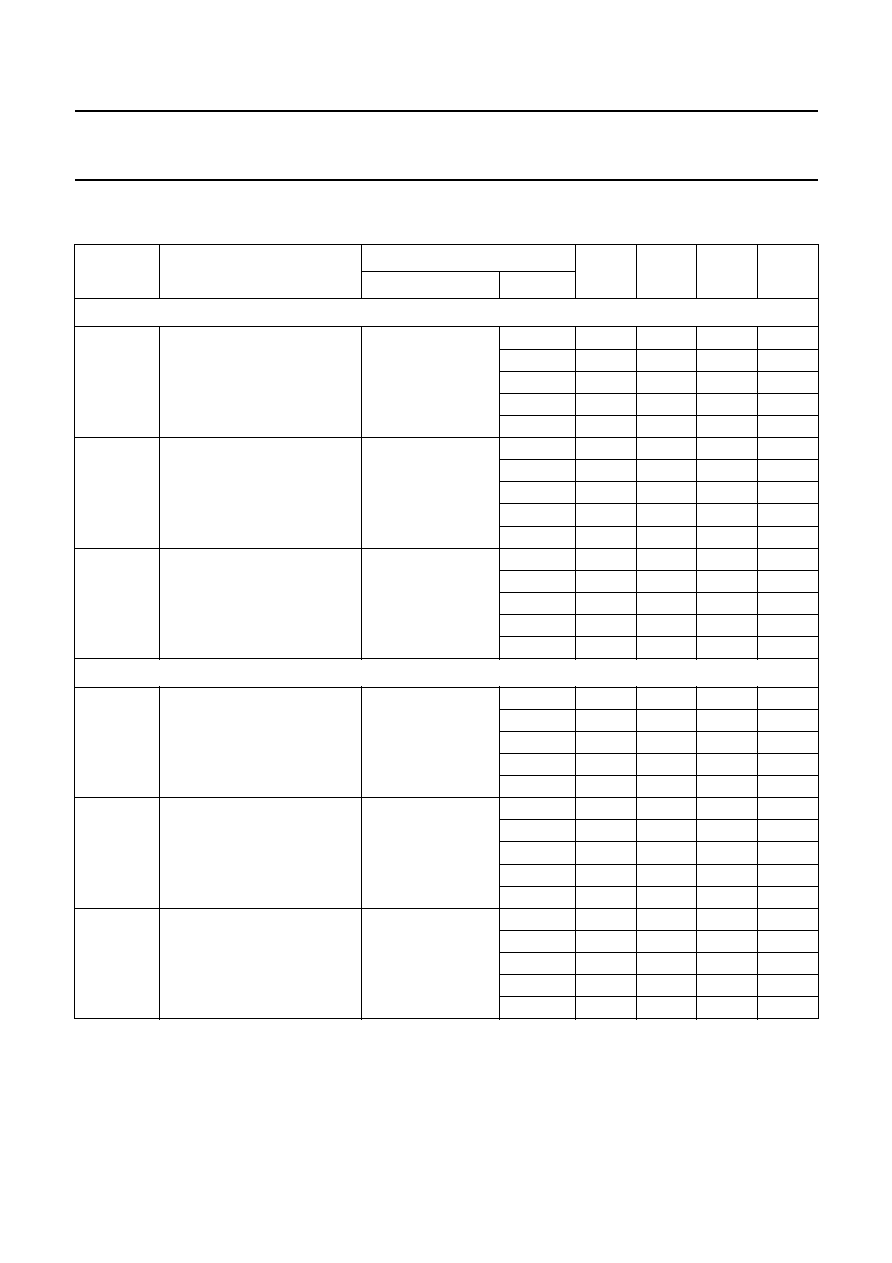
DC CHARACTERISTICS
At recommended operating conditions; voltages are referenced to GND (ground = 0 V).
SYMBOL
PARAMETER
TEST CONDITIONS
MIN.
TYP.
(1)
MAX.
UNIT
OTHER
V
CC
(V)
T
amb
=
-
40 to +85
∞
C
V
OL
LOW-level output voltage V
I
= V
IH
or V
IL
I
O
= 100
µ
A
1.65 to 5.5
-
-
0.1
V
I
O
= 4 mA
1.65
-
-
0.45
V
I
O
= 8 mA
2.3
-
-
0.3
V
I
O
= 12 mA
2.7
-
-
0.4
V
I
O
= 24 mA
3.0
-
-
0.55
V
I
O
= 32 mA
4.5
-
-
0.55
V
V
OH
HIGH-level output
voltage
V
I
= V
IH
or V
IL
I
O
=
-
100
µ
A
1.65 to 5.5
V
CC
-
0.1
-
-
V
I
O
=
-
4 mA
1.65
1.2
-
-
V
I
O
=
-
8 mA
2.3
1.9
-
-
V
I
O
=
-
12 mA
2.7
2.2
-
-
V
I
O
=
-
24 mA
3.0
2.3
-
-
V
I
O
=
-
32 mA
4.5
3.8
-
-
V
I
LI
input leakage current
V
I
= 5.5 V or GND
5.5
-
±
0.1
±
5
µ
A
I
off
power OFF leakage
current
V
I
or V
O
= 5.5 V
0
-
±
0.1
±
10
µ
A
I
CC
quiescent supply current
V
I
= V
CC
or GND;
I
O
= 0
5.5
-
0.1
10
µ
A
I
CC
additional quiescent
supply current per pin
V
I
= V
CC
-
0.6 V;
I
O
= 0
2.3 to 5.5
-
5
500
µ
A

2003 Aug 13
7
Philips Semiconductors
Product specification
Dual non-inverting Schmitt-trigger with
5 V tolerant input
74LVC2G17
Note
1. All typical values are measured at V
CC
= 3.3 V and T
amb
= 25
∞
C.
T
amb
=
-
40 to +125
∞
C
V
OL
LOW-level output voltage V
I
= V
IH
or V
IL
I
O
= 100
µ
A
1.65 to 5.5
-
-
0.1
V
I
O
= 4 mA
1.65
-
-
0.70
V
I
O
= 8 mA
2.3
-
-
0.45
V
I
O
= 12 mA
2.7
-
-
0.60
V
I
O
= 24 mA
3.0
-
-
0.80
V
I
O
= 32 mA
4.5
-
-
0.80
V
V
OH
HIGH-level output
voltage
V
I
= V
IH
or V
IL
I
O
=
-
100
µ
A
1.65 to 5.5
V
CC
-
0.1
-
-
V
I
O
=
-
4 mA
1.65
0.95
-
-
V
I
O
=
-
8 mA
2.3
1.7
-
-
V
I
O
=
-
12 mA
2.7
1.9
-
-
V
I
O
=
-
24 mA
3.0
2.0
-
-
V
I
O
=
-
32 mA
4.5
3.4
-
-
V
I
LI
input leakage current
V
I
= 5.5 V or GND
5.5
-
±
0.1
±
20
µ
A
I
off
power OFF leakage
current
V
I
or V
O
= 5.5 V
0
-
-
±
20
µ
A
I
CC
quiescent supply current
V
I
= V
CC
or GND;
I
O
= 0
5.5
-
-
40
µ
A
I
CC
additional quiescent
supply current per pin
V
I
= V
CC
-
0.6 V;
I
O
= 0
2.3 to 5.5
-
-
5000
µ
A
SYMBOL
PARAMETER
TEST CONDITIONS
MIN.
TYP.
(1)
MAX.
UNIT
OTHER
V
CC
(V)
2003 Aug 13
8
Philips Semiconductors
Product specification
Dual non-inverting Schmitt-trigger with
5 V tolerant input
74LVC2G17
TRANSFER CHARACTERISTICS
Voltages are referenced to GND (ground = 0 V).
Notes
1. All typical values are measured at T
amb
= 25
∞
C.
SYMBOL
PARAMETER
TEST CONDITIONS
MIN.
TYP.
(1)
MAX.
UNIT
WAVEFORMS
V
CC
(V)
T
amb
=
-
40 to +85
∞
C
V
T+
positive-going threshold
see Figs 5 and 6
1.8
0.70
1.10
1.50
V
2.3
1.00
1.40
1.80
V
3.0
1.30
1.76
2.20
V
4.5
1.90
2.47
3.10
V
5.5
2.20
2.91
3.60
V
V
T
-
negative-going threshold
see Figs 5 and 6
1.8
0.25
0.61
0.90
V
2.3
0.40
0.80
1.15
V
3.0
0.60
1.04
1.50
V
4.5
1.00
1.55
2.00
V
5.5
1.20
1.86
2.30
V
V
H
hysteresis (V
T+
-
V
T
-
)
see Figs 5, 6 and 7
1.8
0.15
0.49
1.00
V
2.3
0.25
0.60
1.10
V
3.0
0.40
0.73
1.20
V
4.5
0.60
0.92
1.50
V
5.5
0.70
1.02
1.70
V
T
amb
=
-
40 to +125
∞
C
V
T+
positive-going threshold
see Figs 5 and 6
1.8
0.70
-
1.70
V
2.3
1.00
-
2.00
V
3.0
1.30
-
2.40
V
4.5
1.90
-
3.30
V
5.5
2.20
-
3.80
V
V
T
-
negative-going threshold
see Figs 5 and 6
1.8
0.25
-
1.10
V
2.3
0.40
-
1.35
V
3.0
0.60
-
1.70
V
4.5
1.00
-
2.20
V
5.5
1.20
-
2.50
V
V
H
hysteresis (V
T+
-
V
T
-
)
see Figs 5, 6 and 7
1.8
0.15
-
1.20
V
2.3
0.25
-
1.30
V
3.0
0.40
-
1.40
V
4.5
0.60
-
1.70
V
5.5
0.70
-
1.90
V
2003 Aug 13
9
Philips Semiconductors
Product specification
Dual non-inverting Schmitt-trigger with
5 V tolerant input
74LVC2G17
handbook, halfpage
MNB069
VO
VI
VH
VT
+
VT
-
Fig.5 Transfer characteristic.
handbook, halfpage
MNB070
VO
VI
VH
VT
+
VT
-
Fig.6 Definition of V
T+
, V
T
-
and V
H
.
V
T+
and V
T
-
are between limits of 20% and 70%.
handbook, halfpage
0
0.5
ICC
(mA)
1
2
14
12
8
6
4
2
0
10
1.5
VI (V)
MNB071
Fig.7 Typical 74LVC2G17 transfer characteristic.
V
CC
= 3.0 V.
2003 Aug 13
10
Philips Semiconductors
Product specification
Dual non-inverting Schmitt-trigger with
5 V tolerant input
74LVC2G17
AC CHARACTERISTICS
GND = 0 V.
Note
1. All typical values are measured at T
amb
= 25
∞
C.
SYMBOL
PARAMETER
TEST CONDITIONS
MIN.
TYP.
(1)
MAX.
UNIT
WAVEFORMS
V
CC
(V)
T
amb
=
-
40 to +85
∞
C
t
PHL
/t
PLH
propagation delay nA to nY see Figs 8 and 9
1.65 to 1.95
1.5
5.6
10.5
ns
2.3 to 2.7
1.0
3.7
6.5
ns
2.7
1.0
3.8
6.5
ns
3.0 to 3.6
1.0
3.6
5.7
ns
4.5 to 5.5
1.0
2.7
4.3
ns
T
amb
=
-
40 to +125
∞
C
t
PHL
/t
PLH
propagation delay nA to nY see Figs 8 and 9
1.65 to 1.95
1.5
-
13.1
ns
2.3 to 2.7
1.0
-
8.5
ns
2.7
1.0
-
8.5
ns
3.0 to 3.6
1.0
-
7.1
ns
4.5 to 5.5
1.0
-
5.4
ns
2003 Aug 13
11
Philips Semiconductors
Product specification
Dual non-inverting Schmitt-trigger with
5 V tolerant input
74LVC2G17
AC WAVEFORMS
handbook, halfpage
MNB072
nA input
nY output
tPLH
tPHL
GND
VI
VM
VM
VM
VM
VOH
VOL
Fig.8 The input (nA) to output (nY) propagation delays and the output transition times.
V
OL
and V
OH
are typical output voltage drop that occur with the output load.
V
CC
V
M
INPUT
V
I
t
r
= t
f
1.65 to 1.95 V 0.5
◊
V
CC
V
CC
2.0 ns
2.3 to 2.7 V
0.5
◊
V
CC
V
CC
2.0 ns
2.7 V
1.5 V
2.7 V
2.5 ns
3.0 to 3.6 V
1.5 V
2.7 V
2.5 ns
4.5 to 5.5 V
0.5
◊
V
CC
V
CC
2.5 ns
handbook, full pagewidth
VEXT
VCC
VI
VO
MNA616
D.U.T.
CL
RT
RL
RL
PULSE
GENERATOR
Fig.9 Load circuitry for switching times.
Definitions for test circuit:
R
L
= Load resistor.
C
L
= Load capacitance including jig and probe capacitance.
R
T
= Termination resistance should be equal to the output impedance Z
o
of the pulse generator.
V
CC
V
I
C
L
R
L
V
EXT
t
PLH
/t
PHL
t
PZH
/t
PHZ
t
PZL
/t
PLZ
1.65 to 1.95 V
V
CC
30 pF
1 k
open
GND
2
◊
V
CC
2.3 to 2.7 V
V
CC
30 pF
500
open
GND
2
◊
V
CC
2.7 V
2.7 V
50 pF
500
open
GND
6 V
3.0 to 3.6 V
2.7 V
50 pF
500
open
GND
6 V
4.5 to 5.5 V
V
CC
50 pF
500
open
GND
2
◊
V
CC
2003 Aug 13
12
Philips Semiconductors
Product specification
Dual non-inverting Schmitt-trigger with
5 V tolerant input
74LVC2G17
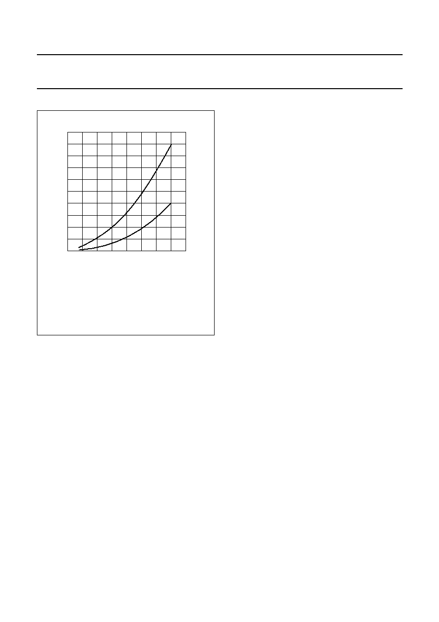
APPLICATION INFORMATION
handbook, halfpage
2
3
4
ICC
(mA)
6
VCC (V)
50
0
40
5
30
20
10
MNB073
Fig.10 Average I
CC
for 74LVC2G17 Schmitt-trigger
devices.
All values given are typical unless otherwise specified.
Linear change of V
I
between 0.8 to 2.0 V.
2003 Aug 13
13
Philips Semiconductors
Product specification
Dual non-inverting Schmitt-trigger with
5 V tolerant input
74LVC2G17
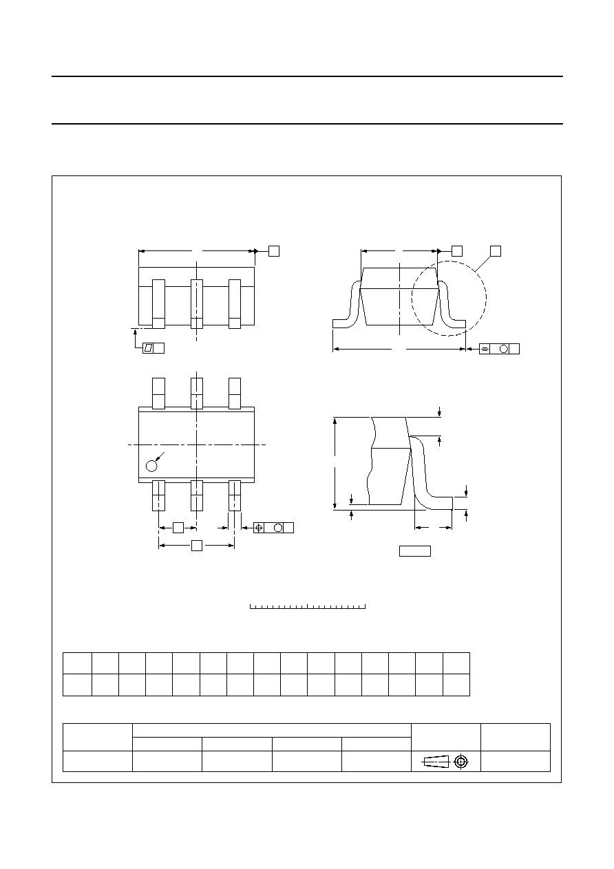
PACKAGE OUTLINES
REFERENCES
OUTLINE
VERSION
EUROPEAN
PROJECTION
ISSUE DATE
IEC
JEDEC
EIAJ
SOT363
SC-88
w
B
M
bp
D
e1
e
pin 1
index
A
A1
Lp
Q
detail X
HE
E
v
M
A
A
B
y
0
1
2 mm
scale
c
X
1
3
2
4
5
6
Plastic surface mounted package; 6 leads
SOT363
UNIT
A1
max
bp
c
D
E
e
1
HE
Lp
Q
y
w
v
mm
0.1
0.30
0.20
2.2
1.8
0.25
0.10
1.35
1.15
0.65
e
1.3
2.2
2.0
0.2
0.1
0.2
DIMENSIONS (mm are the original dimensions)
0.45
0.15
0.25
0.15
A
1.1
0.8
97-02-28

2003 Aug 13
14
Philips Semiconductors
Product specification
Dual non-inverting Schmitt-trigger with
5 V tolerant input
74LVC2G17
REFERENCES
OUTLINE
VERSION
EUROPEAN
PROJECTION
ISSUE DATE
IEC
JEDEC
EIAJ
SOT457
SC-74
w
B
M
bp
D
e
pin 1
index
A
A1
Lp
Q
detail X
HE
E
v
M
A
A
B
y
0
1
2 mm
scale
c
X
1
3
2
4
5
6
Plastic surface mounted package; 6 leads
SOT457
UNIT
A1
bp
c
D
E
HE
Lp
Q
y
w
v
mm
0.1
0.013
0.40
0.25
3.1
2.7
0.26
0.10
1.7
1.3
e
0.95
3.0
2.5
0.2
0.1
0.2
DIMENSIONS (mm are the original dimensions)
0.6
0.2
0.33
0.23
A
1.1
0.9
97-02-28
01-05-04
2003 Aug 13
15
Philips Semiconductors
Product specification
Dual non-inverting Schmitt-trigger with
5 V tolerant input
74LVC2G17
DATA SHEET STATUS
Notes
1. Please consult the most recently issued data sheet before initiating or completing a design.
2. The product status of the device(s) described in this data sheet may have changed since this data sheet was
published. The latest information is available on the Internet at URL http://www.semiconductors.philips.com.
3. For data sheets describing multiple type numbers, the highest-level product status determines the data sheet status.
LEVEL
DATA SHEET
STATUS
(1)
PRODUCT
STATUS
(2)(3)
DEFINITION
I
Objective data
Development
This data sheet contains data from the objective specification for product
development. Philips Semiconductors reserves the right to change the
specification in any manner without notice.
II
Preliminary data Qualification
This data sheet contains data from the preliminary specification.
Supplementary data will be published at a later date. Philips
Semiconductors reserves the right to change the specification without
notice, in order to improve the design and supply the best possible
product.
III
Product data
Production
This data sheet contains data from the product specification. Philips
Semiconductors reserves the right to make changes at any time in order
to improve the design, manufacturing and supply. Relevant changes will
be communicated via a Customer Product/Process Change Notification
(CPCN).
DEFINITIONS
Short-form specification
The data in a short-form
specification is extracted from a full data sheet with the
same type number and title. For detailed information see
the relevant data sheet or data handbook.
Limiting values definition
Limiting values given are in
accordance with the Absolute Maximum Rating System
(IEC 60134). Stress above one or more of the limiting
values may cause permanent damage to the device.
These are stress ratings only and operation of the device
at these or at any other conditions above those given in the
Characteristics sections of the specification is not implied.
Exposure to limiting values for extended periods may
affect device reliability.
Application information
Applications that are
described herein for any of these products are for
illustrative purposes only. Philips Semiconductors make
no representation or warranty that such applications will be
suitable for the specified use without further testing or
modification.
DISCLAIMERS
Life support applications
These products are not
designed for use in life support appliances, devices, or
systems where malfunction of these products can
reasonably be expected to result in personal injury. Philips
Semiconductors customers using or selling these products
for use in such applications do so at their own risk and
agree to fully indemnify Philips Semiconductors for any
damages resulting from such application.
Right to make changes
Philips Semiconductors
reserves the right to make changes in the products -
including circuits, standard cells, and/or software -
described or contained herein in order to improve design
and/or performance. When the product is in full production
(status `Production'), relevant changes will be
communicated via a Customer Product/Process Change
Notification (CPCN). Philips Semiconductors assumes no
responsibility or liability for the use of any of these
products, conveys no licence or title under any patent,
copyright, or mask work right to these products, and
makes no representations or warranties that these
products are free from patent, copyright, or mask work
right infringement, unless otherwise specified.

© Koninklijke Philips Electronics N.V. 2003
SCA75
All rights are reserved. Reproduction in whole or in part is prohibited without the prior written consent of the copyright owner.
The information presented in this document does not form part of any quotation or contract, is believed to be accurate and reliable and may be changed
without notice. No liability will be accepted by the publisher for any consequence of its use. Publication thereof does not convey nor imply any license
under patent- or other industrial or intellectual property rights.
Philips Semiconductors ≠ a worldwide company
Contact information
For additional information please visit http://www.semiconductors.philips.com.
Fax: +31 40 27 24825
For sales offices addresses send e-mail to: sales.addresses@www.semiconductors.philips.com.
Printed in The Netherlands
613508/01/pp
16
Date of release:
2003 Aug 13
Document order number:
9397 750 11688