2003 Nov 25
2
Philips Semiconductors
Product specification
16-bit bus transceiver with direction pin; 5 V tolerant;
3-state
74LVC16245A;
74LVCH16245A
FEATURES
∑
5 V tolerant inputs/outputs for interfacing with 5 V logic
∑
Wide supply voltage range from 1.2 to 3.6 V
∑
CMOS low power consumption
∑
MULTIBYTE
TM
flow-through standard pin-out
architecture
∑
Low inductance multiple power and ground pins for
minimum noise and ground bounce
∑
Direct interface with TTL levels
∑
High-impedance when V
CC
= 0 V
∑
All data inputs have bushold (74LVCH16245A only)
∑
Complies with JEDEC standard no. 8-1A
∑
ESD protection:
HBM EIA/JESD22-A114-A exceeds 2000 V
MM EIA/JESD22-A115-A exceeds 200 V.
DESCRIPTION
The 74LVC(H)16245A is a high-performance, low-power,
low-voltage, Si-gate CMOS device, superior to most
advanced CMOS compatible TTL families. Inputs can be
driven from either 3.3 or 5 V devices. In 3-state operation,
outputs can handle 5 Volt. These features allow the use of
these devices as a mixed 3.3 and 5 V environment.
The 74LVC(H)16245A is a 16-bit transceiver featuring
non-inverting 3-state bus compatible outputs in both send
and receive directions. The device features two output
enable (nOE) inputs for easy cascading and two
send/receive (nDIR) inputs for direction control. nOE
controls the outputs so that the buses are effectively
isolated. This device can be used as two 8-bit transceivers
or one 16-bit transceiver.
The 74LVCH16245A bushold data inputs eliminates the
need for external pull-up resistors to hold unused inputs.
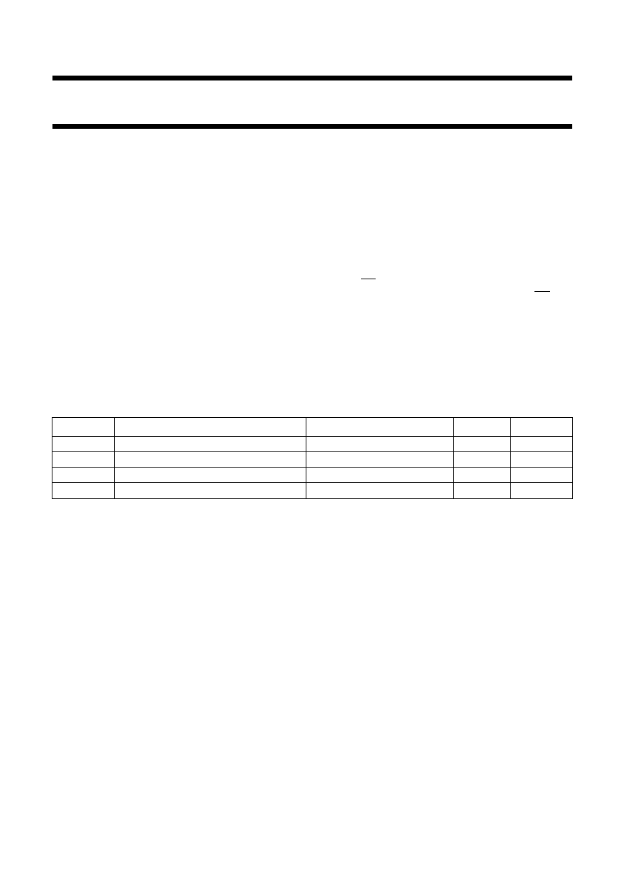
QUICK REFERENCE DATA
GND = 0 V; T
amb
= 25
∞
C; t
r
= t
f
2.5 ns.
Notes
1. C
PD
is used to determine the dynamic power dissipation (P
D
in
µ
W).
P
D
= C
PD
◊
V
CC
2
◊
f
i
◊
N +
(C
L
◊
V
CC
2
◊
f
o
) where:
f
i
= input frequency in MHz;
f
o
= output frequency in MHz;
C
L
= output load capacitance in pF;
V
CC
= supply voltage in Volts;
N = total load switching outputs;
(C
L
◊
V
CC
2
◊
f
o
) = sum of the outputs.
2. The condition is V
I
= GND to V
CC
.
SYMBOL
PARAMETER
CONDITIONS
TYPICAL
UNIT
t
PHL
/t
PLH
propagation delay nAn to nBn; nBn to nAn C
L
= 50 pF; V
CC
= 3.3 V
2.2
ns
C
I
input capacitance
5.0
pF
C
I/O
input/output capacitance
10
pF
C
PD
power dissipation capacitance per gate
V
CC
= 3.3 V; notes 1 and 2
30
pF
2003 Nov 25
3
Philips Semiconductors
Product specification
16-bit bus transceiver with direction pin; 5 V tolerant;
3-state
74LVC16245A;
74LVCH16245A
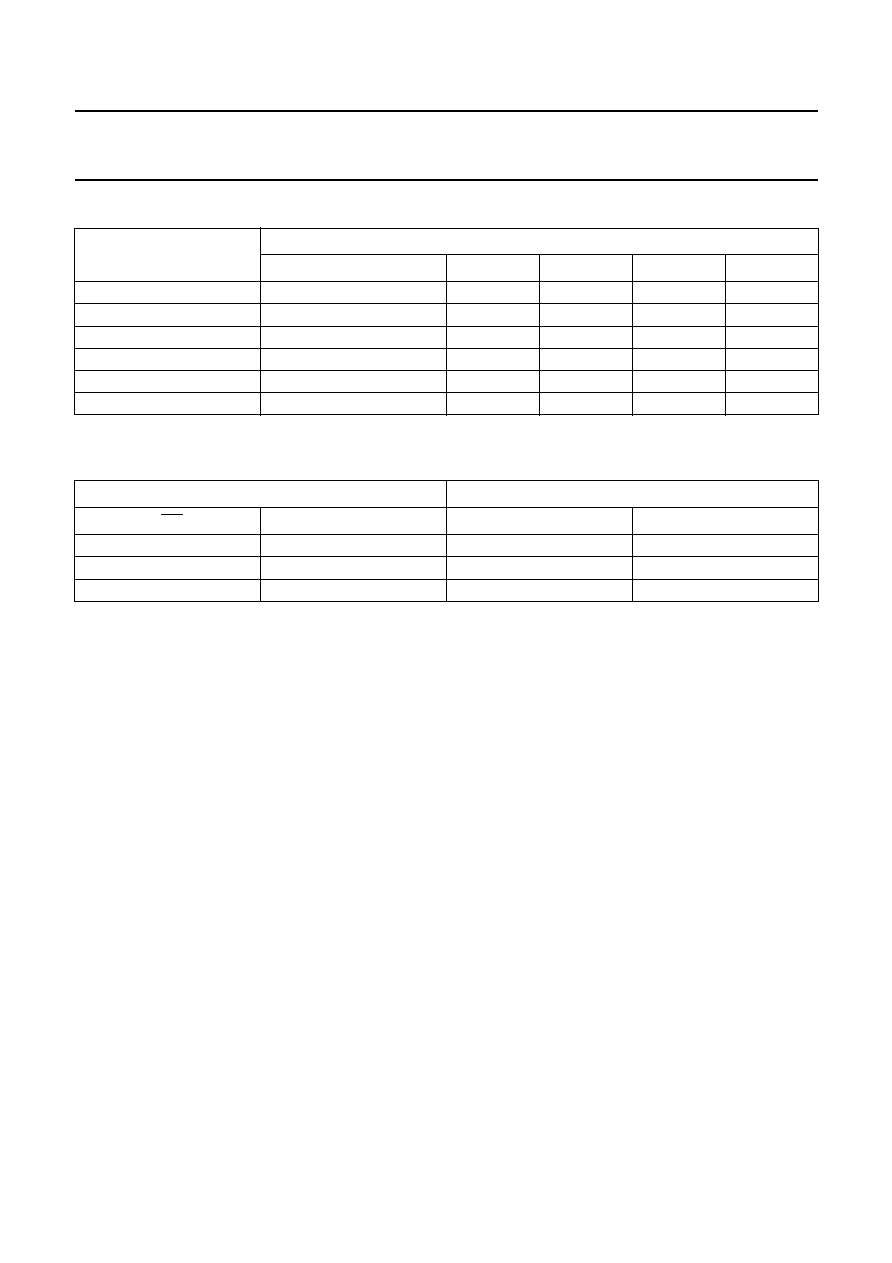
ORDERING INFORMATION
FUNCTION TABLE
See note 1.
Note
1. H = HIGH voltage level;
L = LOW voltage level;
X = don't care;
Z = high-impedance OFF-state.
TYPE NUMBER
PACKAGE
TEMPERATURE RANGE
PINS
PACKAGE
MATERIAL
CODE
74LVC16245ADL
-
40 to +125
∞
C
48
SSOP48
plastic
SOT370-1
74LVCH16245ADL
-
40 to +125
∞
C
48
SSOP48
plastic
SOT370-1
74LVC16245ADGG
-
40 to +125
∞
C
48
TSSOP48
plastic
SOT362-1
74LVCH16245ADGG
-
40 to +125
∞
C
48
TSSOP48
plastic
SOT362-1
74LVC16245AEV
-
40 to +125
∞
C
56
VFBGA56
plastic
SOT702-1
74LVCH16245AEV
-
40 to +125
∞
C
56
VFBGA56
plastic
SOT702-1
INPUT
OUTPUT
nOE
nDIR
nAn
nBn
L
L
A = B
inputs
L
H
inputs
B = A
H
X
Z
Z
2003 Nov 25
4
Philips Semiconductors
Product specification
16-bit bus transceiver with direction pin; 5 V tolerant;
3-state
74LVC16245A;
74LVCH16245A
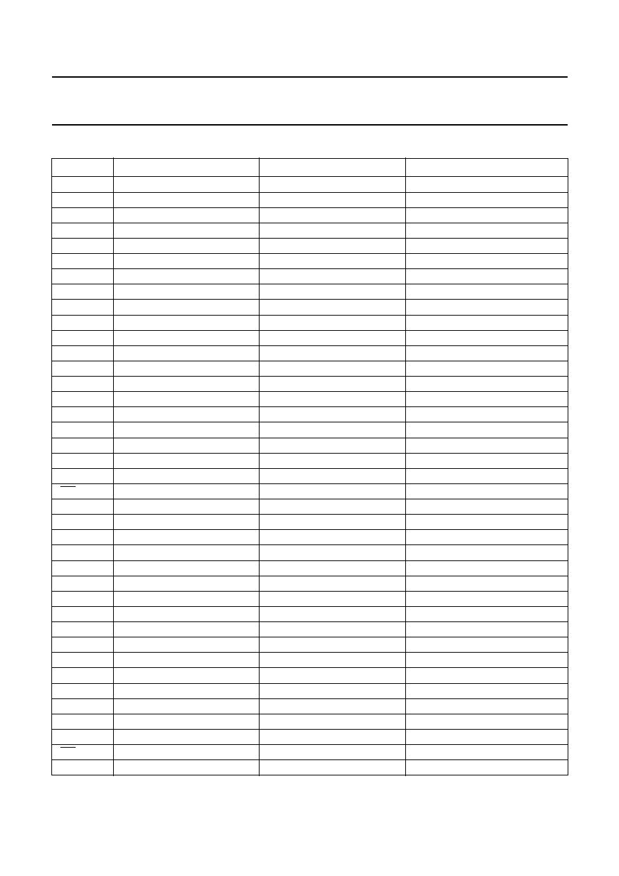
PINNING
SYMBOL
PIN
BALL
DESCRIPTION
1DIR
1
A1
direction control input
1B0
2
B2
data input/output
1B1
3
B1
data input/output
GND
4, 10, 15, 21, 28, 34, 39, 45
B3, B4, D3, D4, G3, G4, J3, J4
ground (0 V)
1B2
5
C2
data input/output
1B3
6
C1
data input/output
V
CC
7, 18, 31, 42
C3, C4, H3, H4
supply voltage
1B4
8
D2
data input/output
1B5
9
D1
data input/output
1B6
11
E2
data input/output
1B7
12
E1
data input/output
2B0
13
F1
data input/output
2B1
14
F2
data input/output
2B2
16
G1
data input/output
2B3
17
G2
data input/output
2B4
19
H1
data input/output
2B5
20
H2
data input/output
2B6
22
J1
data input/output
2B7
23
J2
data input/output
2DIR
24
K1
direction control input
2OE
25
K6
output enable input (active LOW)
2A7
26
J5
data input/output
2A6
27
J6
data input/output
2A5
29
H5
data input/output
2A4
30
H6
data input/output
2A3
32
G5
data input/output
2A2
33
G6
data input/output
2A1
35
F5
data input/output
2A0
36
F6
data input/output
1A7
37
E6
data input/output
1A6
38
E5
data input/output
1A5
40
D6
data input/output
1A4
41
D5
data input/output
1A3
43
C6
data input/output
1A2
44
C5
data input/output
1A1
46
B6
data input/output
1A0
47
B5
data input/output
1OE
48
A6
output enable input (active LOW)
n.c.
-
A2, A3, A4, A5, K2, K3, K4, K5
not connected