ICS8523 Final Data Sheet
8523BG
www.icst.com/products/hiperclocks.html
REV. C OCTOBER 25, 2002
1
Integrated
Circuit
Systems, Inc.
ICS8523
L
OW
S
KEW
, 1-
TO
-4
D
IFFERENTIAL
-
TO
-LVHSTL F
ANOUT
B
UFFER
B
LOCK
D
IAGRAM
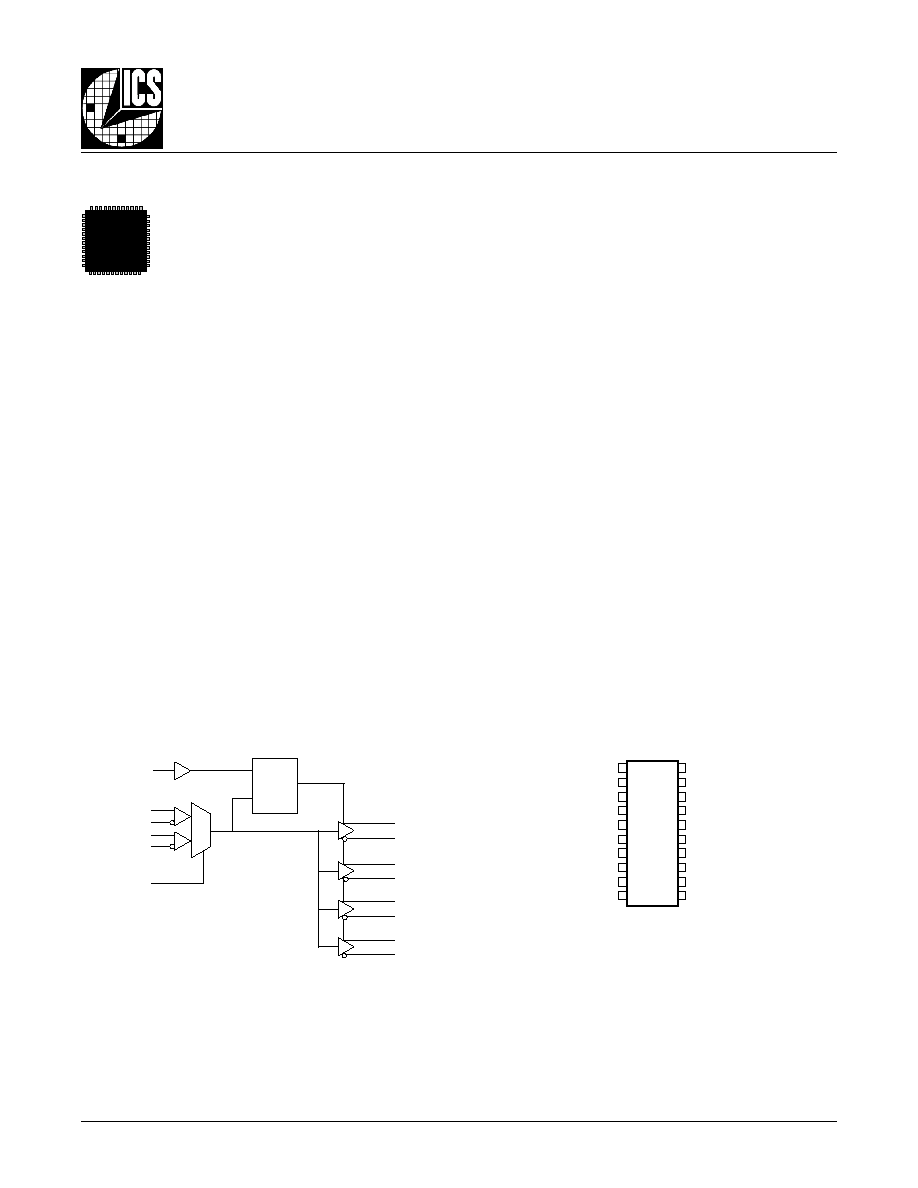
P
IN
A
SSIGNMENT
ICS8523
20-Lead TSSOP
6.5mm x 4.4mm x 0.92mm body package
G Package
Top View
GND
CLK_EN
CLK_SEL
CLK
nCLK
PCLK
nPCLK
nc
nc
V
DD
1
2
3
4
5
6
7
8
9
10
20
19
18
17
16
15
14
13
12
11
Q0
nQ0
V
DDO
Q1
nQ1
Q2
nQ2
V
DDO
Q3
nQ3
G
ENERAL
D
ESCRIPTION
The ICS8523 is a low skew, high perfor-
mance 1-to-4 Differential-to-LVHSTL fanout buffer
and a member of the HiPerClockSTM family of High
Performance Clock Solutions from ICS. The
ICS8523 has two selectable clock inputs. The
CLK, nCLK pair can accept most standard differential input
levels. The PCLK, nPCLK pair can accept LVPECL, CML, or
SSTL input levels. The clock enable is internally synchronized
to eliminate runt pulses on the outputs during asynchronous
assertion/deassertion of the clock enable pin.
Guaranteed output and part-to-part skew characteristics
make the ICS8523 ideal for those applications demanding
well defined performance and repeatability.
F
EATURES
�
4 differential LVHSTL compatible outputs
�
Selectable diffferential CLK, nCLK or LVPECL clock inputs
�
CLK, nCLK pair can accept the following differential
input levels: LVDS, LVPECL, LVHSTL, SSTL, HCSL
�
PCLK, nPCLK supports the following input types:
LVPECL, CML, SSTL
�
Maximum output frequency: 650MHz
�
Translates any single-ended input signal to LVHSTL
levels with resistor bias on nCLK input
�
Output skew: 30ps (maximum)
�
Part-to-part skew: 200ps (maximum)
�
Propagation delay: 1.6ns (maximum)
�
3.3V core, 1.8V output operating supply
�
0�C to 70�C ambient operating temperature
�
Industrial temperature information available upon request
HiPerClockSTM
,&6
CLK
nCLK
PCLK
nPCLK
Q0
nQ0
Q1
nQ1
Q2
nQ2
Q3
nQ3
0
1
CLK_EN
CLK_SEL
D
Q
LE
8523BG
www.icst.com/products/hiperclocks.html
REV. C OCTOBER 25, 2002
2
Integrated
Circuit
Systems, Inc.
ICS8523
L
OW
S
KEW
, 1-
TO
-4
D
IFFERENTIAL
-
TO
-LVHSTL F
ANOUT
B
UFFER
T
ABLE
1. P
IN
D
ESCRIPTIONS
T
ABLE
2. P
IN
C
HARACTERISTICS
l
o
b
m
y
S
r
e
t
e
m
a
r
a
P
s
n
o
i
t
i
d
n
o
C
t
s
e
T
m
u
m
i
n
i
M
l
a
c
i
p
y
T
m
u
m
i
x
a
M
s
t
i
n
U
C
N
I
e
c
n
a
t
i
c
a
p
a
C
t
u
p
n
I
4
F
p
R
P
U
L
L
U
P
r
o
t
s
i
s
e
R
p
u
ll
u
P
t
u
p
n
I
1
5
K
R
N
W
O
D
L
L
U
P
r
o
t
s
i
s
e
R
n
w
o
d
ll
u
P
t
u
p
n
I
1
5
K
r
e
b
m
u
N
e
m
a
N
e
p
y
T
n
o
i
t
p
i
r
c
s
e
D
1
D
N
G
r
e
w
o
P
.
d
n
u
o
r
g
y
l
p
p
u
s
r
e
w
o
P
2
N
E
_
K
L
C
t
u
p
n
I
p
u
ll
u
P
k
c
o
l
c
w
o
ll
o
f
s
t
u
p
t
u
o
k
c
o
l
c
,
H
G
I
H
n
e
h
W
.
e
l
b
a
n
e
k
c
o
l
c
g
n
i
z
i
n
o
r
h
c
n
y
S
d
e
c
r
o
f
e
r
a
s
t
u
p
t
u
o
Q
n
,
w
o
l
d
e
c
r
o
f
e
r
a
s
t
u
p
t
u
o
Q
,
W
O
L
n
e
h
W
.
t
u
p
n
i
.
s
l
e
v
e
l
e
c
a
f
r
e
t
n
i
L
T
T
V
L
/
S
O
M
C
V
L
.
h
g
i
h
3
L
E
S
_
K
L
C
t
u
p
n
I
n
w
o
d
ll
u
P
K
L
C
P
n
,
K
L
C
P
l
a
i
t
n
e
r
e
f
f
i
d
s
t
c
e
l
e
s
,
H
G
I
H
n
e
h
W
.
t
u
p
n
i
t
c
e
l
e
s
k
c
o
l
C
.
s
t
u
p
n
i
K
L
C
n
,
K
L
C
s
t
c
e
l
e
s
,
W
O
L
n
e
h
W
.
s
t
u
p
n
i
.
s
l
e
v
e
l
e
c
a
f
r
e
t
n
i
L
T
T
V
L
/
S
O
M
C
V
L
4
K
L
C
t
u
p
n
I
n
w
o
d
ll
u
P
.
t
u
p
n
i
k
c
o
l
c
l
a
i
t
n
e
r
e
f
f
i
d
g
n
i
t
r
e
v
n
i
-
n
o
N
5
K
L
C
n
t
u
p
n
I
p
u
ll
u
P
.
t
u
p
n
i
k
c
o
l
c
l
a
i
t
n
e
r
e
f
f
i
d
g
n
i
t
r
e
v
n
I
6
K
L
C
P
t
u
p
n
I
n
w
o
d
ll
u
P
.
t
u
p
n
i
k
c
o
l
c
L
C
E
P
V
L
l
a
i
t
n
e
r
e
f
f
i
d
g
n
i
t
r
e
v
n
i
-
n
o
N
7
K
L
C
P
n
t
u
p
n
I
p
u
ll
u
P
.
t
u
p
n
i
k
c
o
l
c
L
C
E
P
V
L
l
a
i
t
n
e
r
e
f
f
i
d
g
n
i
t
r
e
v
n
I
9
,
8
c
n
d
e
s
u
n
U
.
t
c
e
n
n
o
c
o
N
0
1
V
D
D
r
e
w
o
P
.
n
i
p
y
l
p
p
u
s
e
r
o
C
2
1
,
1
1
3
Q
,
3
Q
n
t
u
p
t
u
O
.
s
l
e
v
e
l
e
c
a
f
r
e
t
n
i
L
T
S
H
V
L
.
r
i
a
p
t
u
p
t
u
o
l
a
i
t
n
e
r
e
f
f
i
D
8
1
,
3
1
V
O
D
D
r
e
w
o
P
.
s
n
i
p
y
l
p
p
u
s
t
u
p
t
u
O
5
1
,
4
1
2
Q
,
2
Q
n
t
u
p
t
u
O
.
s
l
e
v
e
l
e
c
a
f
r
e
t
n
i
L
T
S
H
V
L
.
r
i
a
p
t
u
p
t
u
o
l
a
i
t
n
e
r
e
f
f
i
D
7
1
,
6
1
1
Q
,
1
Q
n
t
u
p
t
u
O
.
s
l
e
v
e
l
e
c
a
f
r
e
t
n
i
L
T
S
H
V
L
.
r
i
a
p
t
u
p
t
u
o
l
a
i
t
n
e
r
e
f
f
i
D
0
2
,
9
1
0
Q
,
0
Q
n
t
u
p
t
u
O
.
s
l
e
v
e
l
e
c
a
f
r
e
t
n
i
L
T
S
H
V
L
.
r
i
a
p
t
u
p
t
u
o
l
a
i
t
n
e
r
e
f
f
i
D
:
E
T
O
N
p
u
ll
u
P
d
n
a
n
w
o
d
ll
u
P
.
s
e
u
l
a
v
l
a
c
i
p
y
t
r
o
f
,
s
c
i
t
s
i
r
e
t
c
a
r
a
h
C
n
i
P
,
2
e
l
b
a
T
e
e
S
.
s
r
o
t
s
i
s
e
r
t
u
p
n
i
l
a
n
r
e
t
n
i
o
t
r
e
f
e
r
8523BG
www.icst.com/products/hiperclocks.html
REV. C OCTOBER 25, 2002
3
Integrated
Circuit
Systems, Inc.
ICS8523
L
OW
S
KEW
, 1-
TO
-4
D
IFFERENTIAL
-
TO
-LVHSTL F
ANOUT
B
UFFER
T
ABLE
3A. C
ONTROL
I
NPUT
F
UNCTION
T
ABLE
T
ABLE
3B. C
LOCK
I
NPUT
F
UNCTION
T
ABLE
s
t
u
p
n
I
s
t
u
p
t
u
O
e
d
o
M
t
u
p
t
u
O
o
t
t
u
p
n
I
y
t
i
r
a
l
o
P
K
L
C
P
r
o
K
L
C
K
L
C
P
n
r
o
K
L
C
n
3
Q
:
0
Q
3
Q
n
:
0
Q
n
0
0
W
O
L
H
G
I
H
l
a
i
t
n
e
r
e
f
f
i
D
o
t
l
a
i
t
n
e
r
e
f
f
i
D
g
n
i
t
r
e
v
n
I
n
o
N
1
1
H
G
I
H
W
O
L
l
a
i
t
n
e
r
e
f
f
i
D
o
t
l
a
i
t
n
e
r
e
f
f
i
D
g
n
i
t
r
e
v
n
I
n
o
N
0
1
E
T
O
N
;
d
e
s
a
i
B
W
O
L
H
G
I
H
l
a
i
t
n
e
r
e
f
f
i
D
o
t
d
e
d
n
E
e
l
g
n
i
S
g
n
i
t
r
e
v
n
I
n
o
N
1
1
E
T
O
N
;
d
e
s
a
i
B
H
G
I
H
W
O
L
l
a
i
t
n
e
r
e
f
f
i
D
o
t
d
e
d
n
E
e
l
g
n
i
S
g
n
i
t
r
e
v
n
I
n
o
N
1
E
T
O
N
;
d
e
s
a
i
B
0
H
G
I
H
W
O
L
l
a
i
t
n
e
r
e
f
f
i
D
o
t
d
e
d
n
E
e
l
g
n
i
S
g
n
i
t
r
e
v
n
I
1
E
T
O
N
;
d
e
s
a
i
B
1
W
O
L
H
G
I
H
l
a
i
t
n
e
r
e
f
f
i
D
o
t
d
e
d
n
E
e
l
g
n
i
S
g
n
i
t
r
e
v
n
I
.
"
s
l
e
v
e
L
d
e
d
n
E
e
l
g
n
i
S
t
p
e
c
c
A
o
t
t
u
p
n
I
l
a
i
t
n
e
r
e
f
f
i
D
e
h
t
g
n
i
r
i
W
"
,
n
o
i
t
c
e
s
n
o
i
t
a
m
r
o
f
n
I
n
o
i
t
a
c
il
p
p
A
e
h
t
o
t
r
e
f
e
r
e
s
a
e
l
P
:
1
E
T
O
N
F
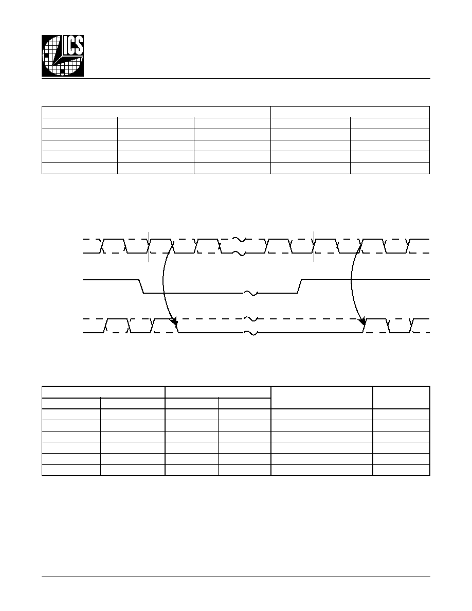
IGURE
1. CLK_EN T
IMING
D
IAGRAM
Enabled
Disabled
nCLK, nPCLK
CLK, PCLK
CLK_EN
nQ0:nQ3
Q0:Q3
s
t
u
p
n
I
s
t
u
p
t
u
O
N
E
_
K
L
C
L
E
S
_
K
L
C
e
c
r
u
o
S
d
e
t
c
e
l
e
S
3
Q
:
0
Q
3
Q
n
:
0
Q
n
0
0
K
L
C
n
,
K
L
C
W
O
L
;
d
e
l
b
a
s
i
D
H
G
I
H
;
d
e
l
b
a
s
i
D
0
1
K
L
C
P
n
,
K
L
C
P
W
O
L
;
d
e
l
b
a
s
i
D
H
G
I
H
;
d
e
l
b
a
s
i
D
1
0
K
L
C
n
,
K
L
C
d
e
l
b
a
n
E
d
e
l
b
a
n
E
1
1
K
L
C
P
n
,
K
L
C
P
d
e
l
b
a
n
E
d
e
l
b
a
n
E
e
g
d
e
k
c
o
l
c
t
u
p
n
i
g
n
il
l
a
f
d
n
a
g
n
i
s
i
r
a
g
n
i
w
o
ll
o
f
d
e
l
b
a
n
e
r
o
d
e
l
b
a
s
i
d
e
r
a
s
t
u
p
t
u
o
k
c
o
l
c
e
h
t
,
s
e
h
c
t
i
w
s
N
E
_
K
L
C
r
e
t
f
A
.
1
e
r
u
g
i
F
n
i
n
w
o
h
s
s
a
d
e
b
i
r
c
s
e
d
s
a
s
t
u
p
n
i
K
L
C
P
n
,
K
L
C
P
d
n
a
K
L
C
n
,
K
L
C
e
h
t
f
o
n
o
i
t
c
n
u
f
a
e
r
a
s
t
u
p
t
u
o
e
h
t
f
o
e
t
a
t
s
e
h
t
,
e
d
o
m
e
v
i
t
c
a
e
h
t
n
I
.
B
3
e
l
b
a
T
n
i
8523BG
www.icst.com/products/hiperclocks.html
REV. C OCTOBER 25, 2002
4
Integrated
Circuit
Systems, Inc.
ICS8523
L
OW
S
KEW
, 1-
TO
-4
D
IFFERENTIAL
-
TO
-LVHSTL F
ANOUT
B
UFFER
T
ABLE
4A. P
OWER
S
UPPLY
DC C
HARACTERISTICS
,
V
DD
= 3.3V�5%, V
DDO
= 1.8V�0.2V, T
A
= 0�C
TO
70�C
T
ABLE
4B. LVCMOS / LVTTL DC C
HARACTERISTICS
,
V
DD
= 3.3V�5%, V
DDO
= 1.8V�0.2V, T
A
= 0�C
TO
70�C
T
ABLE
4C. D
IFFERENTIAL
DC C
HARACTERISTICS
,
V
DD
= 3.3V�5%, V
DDO
= 1.8V�0.2V, T
A
= 0�C
TO
70�C
l
o
b
m
y
S
r
e
t
e
m
a
r
a
P
s
n
o
i
t
i
d
n
o
C
t
s
e
T
m
u
m
i
n
i
M
l
a
c
i
p
y
T
m
u
m
i
x
a
M
s
t
i
n
U
V
D
D
e
g
a
t
l
o
V
y
l
p
p
u
S
r
e
w
o
P
e
r
o
C
5
3
1
.
3
3
.
3
5
6
4
.
3
V
V
O
D
D
e
g
a
t
l
o
V
y
l
p
p
u
S
r
e
w
o
P
t
u
p
t
u
O
6
.
1
8
.
1
0
.
2
V
I
D
D
t
n
e
r
r
u
C
y
l
p
p
u
S
r
e
w
o
P
0
5
A
m
l
o
b
m
y
S
r
e
t
e
m
a
r
a
P
s
n
o
i
t
i
d
n
o
C
t
s
e
T
m
u
m
i
n
i
M
l
a
c
i
p
y
T
m
u
m
i
x
a
M
s
t
i
n
U
V
H
I
e
g
a
t
l
o
V
h
g
i
H
t
u
p
n
I
L
E
S
_
K
L
C
,
N
E
_
K
L
C
2
5
6
7
.
3
V
V
L
I
e
g
a
t
l
o
V
w
o
L
t
u
p
n
I
L
E
S
_
K
L
C
,
N
E
_
K
L
C
3
.
0
-
8
.
0
V
I
H
I
t
n
e
r
r
u
C
h
g
i
H
t
u
p
n
I
N
E
_
K
L
C
V
D
D
V
=
N
I
V
5
6
4
.
3
=
5
A
�
L
E
S
_
K
L
C
V
D
D
V
=
N
I
V
5
6
4
.
3
=
0
5
1
A
�
I
L
I
t
n
e
r
r
u
C
w
o
L
t
u
p
n
I
N
E
_
K
L
C
V
D
D
V
,
V
5
6
4
.
3
=
N
I
V
0
=
0
5
1
-
A
�
L
E
S
_
K
L
C
V
D
D
V
,
V
5
6
4
.
3
=
N
I
V
0
=
5
-
A
�
l
o
b
m
y
S
r
e
t
e
m
a
r
a
P
s
n
o
i
t
i
d
n
o
C
t
s
e
T
m
u
m
i
n
i
M
l
a
c
i
p
y
T
m
u
m
i
x
a
M
s
t
i
n
U
I
H
I
t
n
e
r
r
u
C
h
g
i
H
t
u
p
n
I
K
L
C
n
V
D
D
V
=
N
I
V
5
6
4
.
3
=
5
A
�
K
L
C
V
D
D
V
=
N
I
V
5
6
4
.
3
=
0
5
1
A
�
I
L
I
t
n
e
r
r
u
C
w
o
L
t
u
p
n
I
K
L
C
n
V
D
D
V
,
V
5
6
4
.
3
=
N
I
V
0
=
0
5
1
-
A
�
K
L
C
V
D
D
V
,
V
5
6
4
.
3
=
N
I
V
0
=
5
-
A
�
V
P
P
e
g
a
t
l
o
V
t
u
p
n
I
k
a
e
P
-
o
t
-
k
a
e
P
5
1
.
0
3
.
1
V
V
R
M
C
;
e
g
a
t
l
o
V
t
u
p
n
I
e
d
o
M
n
o
m
m
o
C
2
,
1
E
T
O
N
5
.
0
V
D
D
5
8
.
0
-
V
V
s
i
K
L
C
n
d
n
a
K
L
C
r
o
f
e
g
a
t
l
o
v
t
u
p
n
i
m
u
m
i
x
a
m
e
h
t
s
n
o
i
t
a
c
il
p
p
a
d
e
d
n
e
e
l
g
n
i
s
r
o
F
:
1
E
T
O
N
D
D
.
V
3
.
0
+
V
s
a
d
e
n
i
f
e
d
s
i
e
g
a
t
l
o
v
e
d
o
m
n
o
m
m
o
C
:
2
E
T
O
N
H
I
.
A
BSOLUTE
M
AXIMUM
R
ATINGS
Supply Voltage, V
DD
X
4.6V
Inputs, V
DD
-0.5V to V
DD
+ 0.5 V
Outputs, V
DDO
-0.5V to V
DDO
+ 0.5V
Package Thermal Impedance,
JA
73.2�C/W (0 lfpm)
Storage Temperature, T
STG
-65�C to 150�C
NOTE: Stresses beyond those listed under Absolute
Maximum Ratings may cause permanent damage to the
device. These ratings are stress specifications only. Functional
operation of product at these conditions or any conditions be-
yond those listed in the
DC Characteristics or AC Character-
istics is not implied. Exposure to absolute maximum rating
conditions for extended periods may affect product reliability.
8523BG
www.icst.com/products/hiperclocks.html
REV. C OCTOBER 25, 2002
5
Integrated
Circuit
Systems, Inc.
ICS8523
L
OW
S
KEW
, 1-
TO
-4
D
IFFERENTIAL
-
TO
-LVHSTL F
ANOUT
B
UFFER
T
ABLE
4D. LVPECL DC C
HARACTERISTICS
,
V
DD
= 3.3V�5%, V
DDO
= 1.8V�0.2V, T
A
= 0�C
TO
70�C
T
ABLE
5. AC C
HARACTERISTICS
,
V
DD
= 3.3V�5%, V
DDO
= 1.8V�0.2V, T
A
= 0�C
TO
70�C
l
o
b
m
y
S
r
e
t
e
m
a
r
a
P
s
n
o
i
t
i
d
n
o
C
t
s
e
T
m
u
m
i
n
i
M
l
a
c
i
p
y
T
m
u
m
i
x
a
M
s
t
i
n
U
I
H
I
t
n
e
r
r
u
C
h
g
i
H
t
u
p
n
I
K
L
C
P
V
D
D
V
=
N
I
V
5
6
4
.
3
=
0
5
1
A
�
K
L
C
P
n
V
D
D
V
=
N
I
V
5
6
4
.
3
=
5
A
�
I
L
I
t
n
e
r
r
u
C
w
o
L
t
u
p
n
I
K
L
C
P
V
D
D
V
,
V
5
6
4
.
3
=
N
I
V
0
=
5
-
A
�
K
L
C
P
n
V
D
D
V
,
V
5
6
4
.
3
=
N
I
V
0
=
0
5
1
-
A
�
V
P
P
e
g
a
t
l
o
V
t
u
p
n
I
k
a
e
P
-
o
t
-
k
a
e
P
3
.
0
1
V
V
R
M
C
2
,
1
E
T
O
N
;
e
g
a
t
l
o
V
t
u
p
n
I
e
d
o
M
n
o
m
m
o
C
5
.
1
V
D
D
V
V
s
a
d
e
n
i
f
e
d
s
i
e
g
a
t
l
o
v
e
d
o
m
n
o
m
m
o
C
:
1
E
T
O
N
H
I
.
V
s
i
K
L
C
P
n
d
n
a
K
L
C
P
r
o
f
e
g
a
t
l
o
v
t
u
p
n
i
m
u
m
i
x
a
m
e
h
t
s
n
o
i
t
a
c
il
p
p
a
d
e
d
n
e
e
l
g
n
i
s
r
o
F
:
2
E
T
O
N
D
D
.
V
3
.
0
+
l
o
b
m
y
S
r
e
t
e
m
a
r
a
P
s
n
o
i
t
i
d
n
o
C
t
s
e
T
m
u
m
i
n
i
M
l
a
c
i
p
y
T
m
u
m
i
x
a
M
s
t
i
n
U
f
X
A
M
y
c
n
e
u
q
e
r
F
t
u
p
t
u
O
0
5
6
z
H
M
t
D
P
1
E
T
O
N
;
y
a
l
e
D
n
o
i
t
a
g
a
p
o
r
P
z
H
M
0
5
6
0
.
1
6
.
1
s
n
t
)
o
(
k
s
4
,
2
E
T
O
N
;
w
e
k
S
t
u
p
t
u
O
0
3
s
p
t
)
p
p
(
k
s
4
,
3
E
T
O
N
;
w
e
k
S
t
r
a
P
-
o
t
-
t
r
a
P
0
0
2
s
p
t
R
e
m
i
T
e
s
i
R
t
u
p
t
u
O
z
H
M
0
5
@
%
0
8
o
t
%
0
2
0
0
3
0
0
7
s
p
t
F
e
m
i
T
ll
a
F
t
u
p
t
u
O
z
H
M
0
5
@
%
0
8
o
t
%
0
2
0
0
3
0
0
7
s
p
c
d
o
e
l
c
y
C
y
t
u
D
t
u
p
t
u
O
5
4
5
5
%
.
e
s
i
w
r
e
h
t
o
d
e
t
o
n
s
s
e
l
n
u
z
H
M
0
0
5
t
a
d
e
r
u
s
a
e
m
s
r
e
t
e
m
a
r
a
p
ll
A
.
r
e
t
t
ij
d
d
a
t
o
n
s
e
o
d
t
r
a
p
e
h
T
.
t
u
p
t
u
o
e
h
t
n
o
r
e
t
t
ij
e
h
t
l
a
u
q
e
ll
i
w
t
u
p
n
i
e
h
t
n
o
r
e
t
t
ij
e
l
c
y
c
o
t
e
l
c
y
c
e
h
T
.
t
n
i
o
p
g
n
i
s
s
o
r
c
t
u
p
t
u
o
l
a
i
t
n
e
r
e
f
f
i
d
e
h
t
o
t
t
n
i
o
p
g
n
i
s
s
o
r
c
t
u
p
n
i
l
a
i
t
n
e
r
e
f
f
i
d
e
h
t
m
o
r
f
d
e
r
u
s
a
e
M
:
1
E
T
O
N
.
s
n
o
i
t
i
d
n
o
c
d
a
o
l
l
a
u
q
e
h
t
i
w
d
n
a
e
g
a
t
l
o
v
y
l
p
p
u
s
e
m
a
s
e
h
t
t
a
s
t
u
p
t
u
o
n
e
e
w
t
e
b
w
e
k
s
s
a
d
e
n
i
f
e
D
:
2
E
T
O
N
.
s
t
n
i
o
p
s
s
o
r
c
l
a
i
t
n
e
r
e
f
f
i
d
t
u
p
t
u
o
t
a
d
e
r
u
s
a
e
M
s
e
g
a
t
l
o
v
y
l
p
p
u
s
e
m
a
s
e
h
t
t
a
g
n
i
t
a
r
e
p
o
s
e
c
i
v
e
d
t
n
e
r
e
f
f
i
d
n
o
s
t
u
p
t
u
o
n
e
e
w
t
e
b
w
e
k
s
s
a
d
e
n
i
f
e
D
:
3
E
T
O
N
d
e
r
u
s
a
e
m
e
r
a
s
t
u
p
t
u
o
e
h
t
,
e
c
i
v
e
d
h
c
a
e
n
o
s
t
u
p
n
i
f
o
e
p
y
t
e
m
a
s
e
h
t
g
n
i
s
U
.
s
n
o
i
t
i
d
n
o
c
d
a
o
l
l
a
u
q
e
h
t
i
w
d
n
a
.
s
t
n
i
o
p
s
s
o
r
c
l
a
i
t
n
e
r
e
f
f
i
d
e
h
t
t
a
.
5
6
d
r
a
d
n
a
t
S
C
E
D
E
J
h
t
i
w
e
c
n
a
d
r
o
c
c
a
n
i
d
e
n
i
f
e
d
s
i
r
e
t
e
m
a
r
a
p
s
i
h
T
:
4
E
T
O
N
T
ABLE
4D. LVHSTL DC C
HARACTERISTICS
,
V
DD
= 3.3V�5%, V
DDO
= 1.8V�0.2V, T
A
= 0�C
TO
70�C
l
o
b
m
y
S
r
e
t
e
m
a
r
a
P
s
n
o
i
t
i
d
n
o
C
t
s
e
T
m
u
m
i
n
i
M
l
a
c
i
p
y
T
m
u
m
i
x
a
M
s
t
i
n
U
V
H
O
;
e
g
a
t
l
o
V
h
g
i
H
t
u
p
t
u
O
1
E
T
O
N
1
4
.
1
V
V
L
O
;
e
g
a
t
l
o
V
w
o
L
t
u
p
t
u
O
1
E
T
O
N
0
4
.
0
V
V
X
O
e
g
a
t
l
o
V
r
e
v
o
s
s
o
r
C
t
u
p
t
u
O
(
x
%
0
4
V
H
O
- V
L
O
+
)
V
L
O
V
(
x
%
0
6
H
O
V
-
L
O
V
+
)
L
O
V
V
G
N
I
W
S
k
a
e
P
-
o
t
-
k
a
e
P
g
n
i
w
S
e
g
a
t
l
o
V
t
u
p
t
u
O
5
7
.
0
5
2
.
1
V
0
5
h
t
i
w
d
e
t
a
n
i
m
r
e
t
s
t
u
p
t
u
O
:
1
E
T
O
N
.
d
n
u
o
r
g
o
t
8523BG
www.icst.com/products/hiperclocks.html
REV. C OCTOBER 25, 2002
6
Integrated
Circuit
Systems, Inc.
ICS8523
L
OW
S
KEW
, 1-
TO
-4
D
IFFERENTIAL
-
TO
-LVHSTL F
ANOUT
B
UFFER
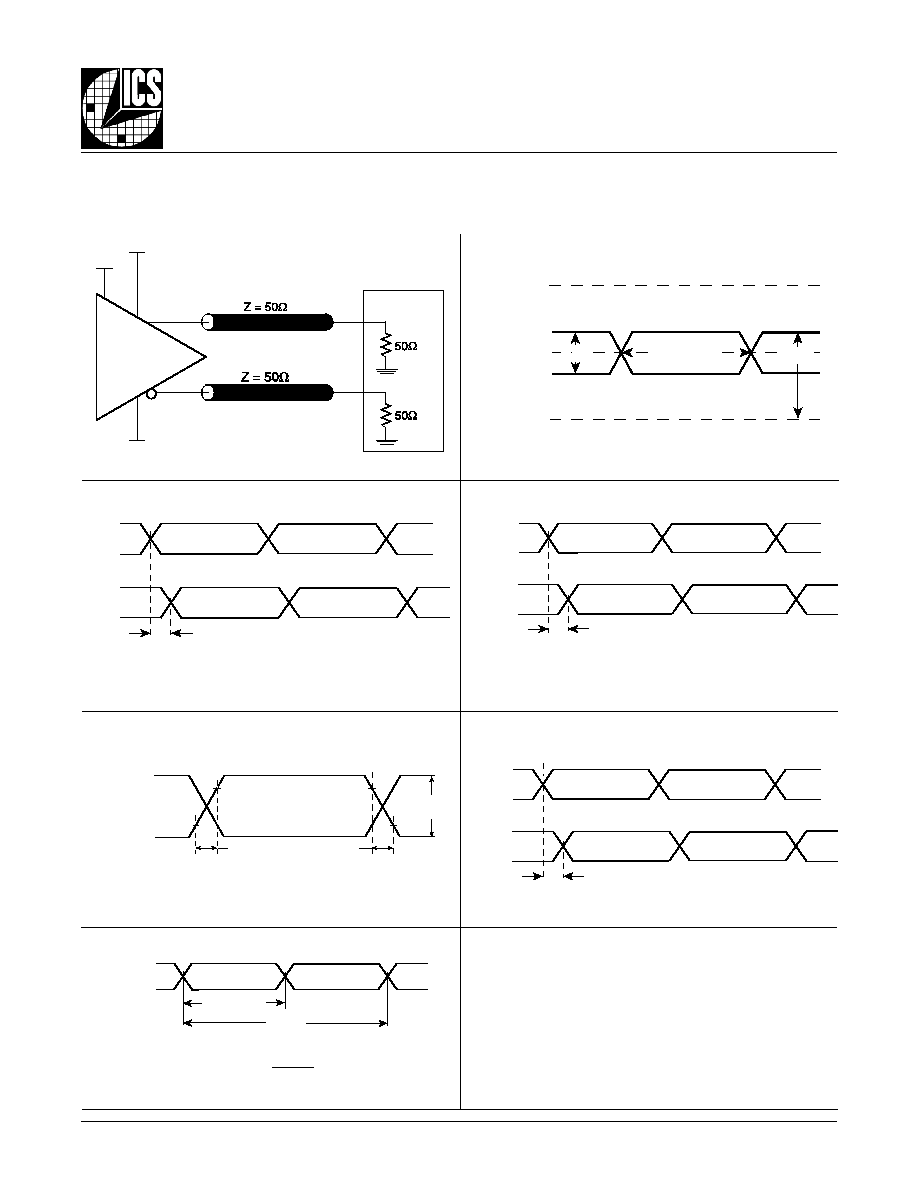
Clock Outputs
20%
80%
80%
20%
t
R
t
F
V
SW I N G
Pulse Width
t
PERIOD
t
PW
t
PERIOD
odc =
nQ0:nQ3
Q0:Q3
t
PD
nCLK,
nPCLK
CLK,
PCLK
nQ0:nQ3
Q0:Q3
Qx
nQx
Qy
nQy
PART 1
PART 2
tsk(pp)
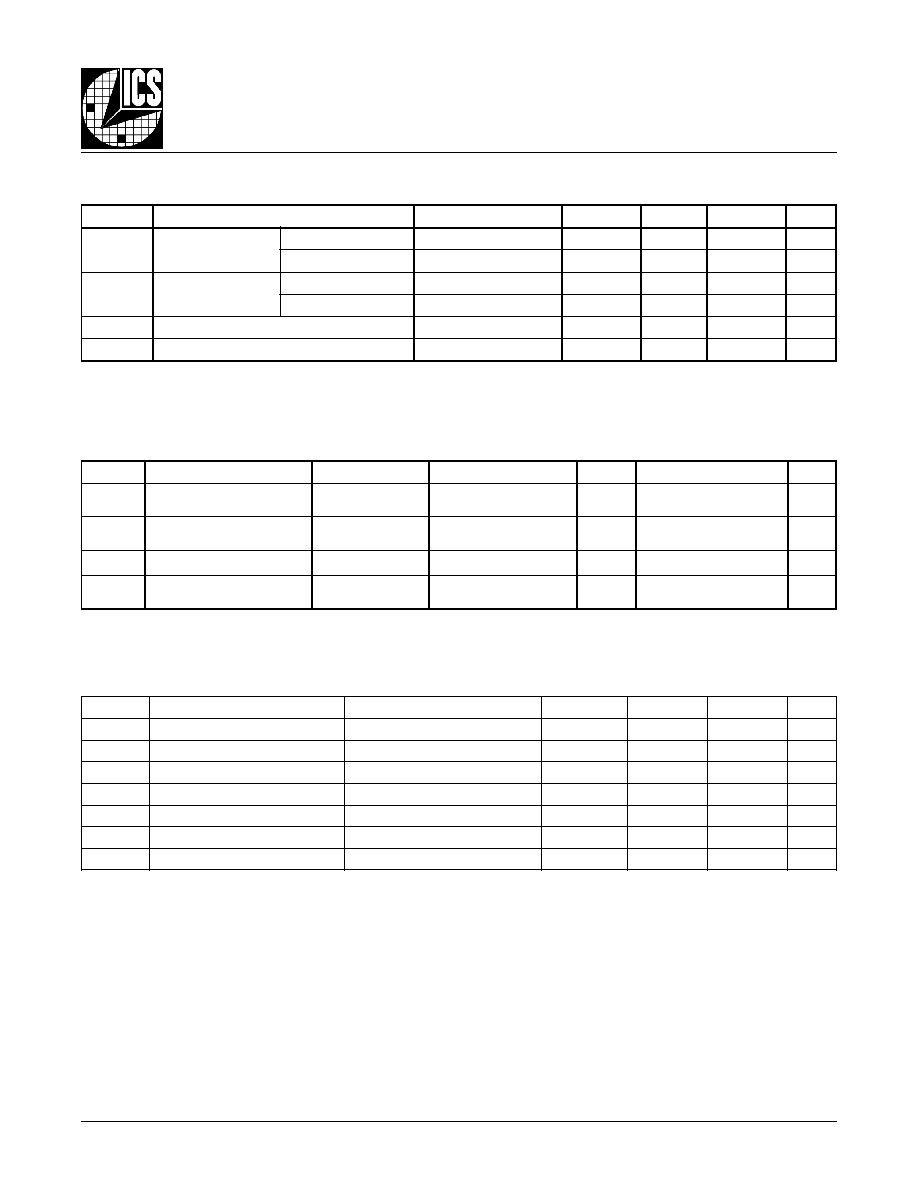
3.3V/1.8V O
UTPUT
L
OAD
AC T
EST
C
IRCUIT
D
IFFERENTIAL
I
NPUT
L
EVEL
P
ART
-
TO
-P
ART
S
KEW
O
UTPUT
S
KEW
odc & t
P
ERIOD
O
UTPUT
R
ISE
/F
ALL
T
IME
P
ROPAGATION
D
ELAY
P
ARAMETER
M
EASUREMENT
I
NFORMATION
tsk(o)
nQx
Qx
nQy
Qy
V
CMR
Cross Points
V
PP
nCLK, nPCLK
CLK, PCLK
GND
V
DD
SCOPE
LVHSTL
Qx
nQx
3.3V�5%
V
DDO
V
DD
GND = 0V
1.8V�0.2V
8523BG
www.icst.com/products/hiperclocks.html
REV. C OCTOBER 25, 2002
7
Integrated
Circuit
Systems, Inc.
ICS8523
L
OW
S
KEW
, 1-
TO
-4
D
IFFERENTIAL
-
TO
-LVHSTL F
ANOUT
B
UFFER
A
PPLICATION
I
NFORMATION
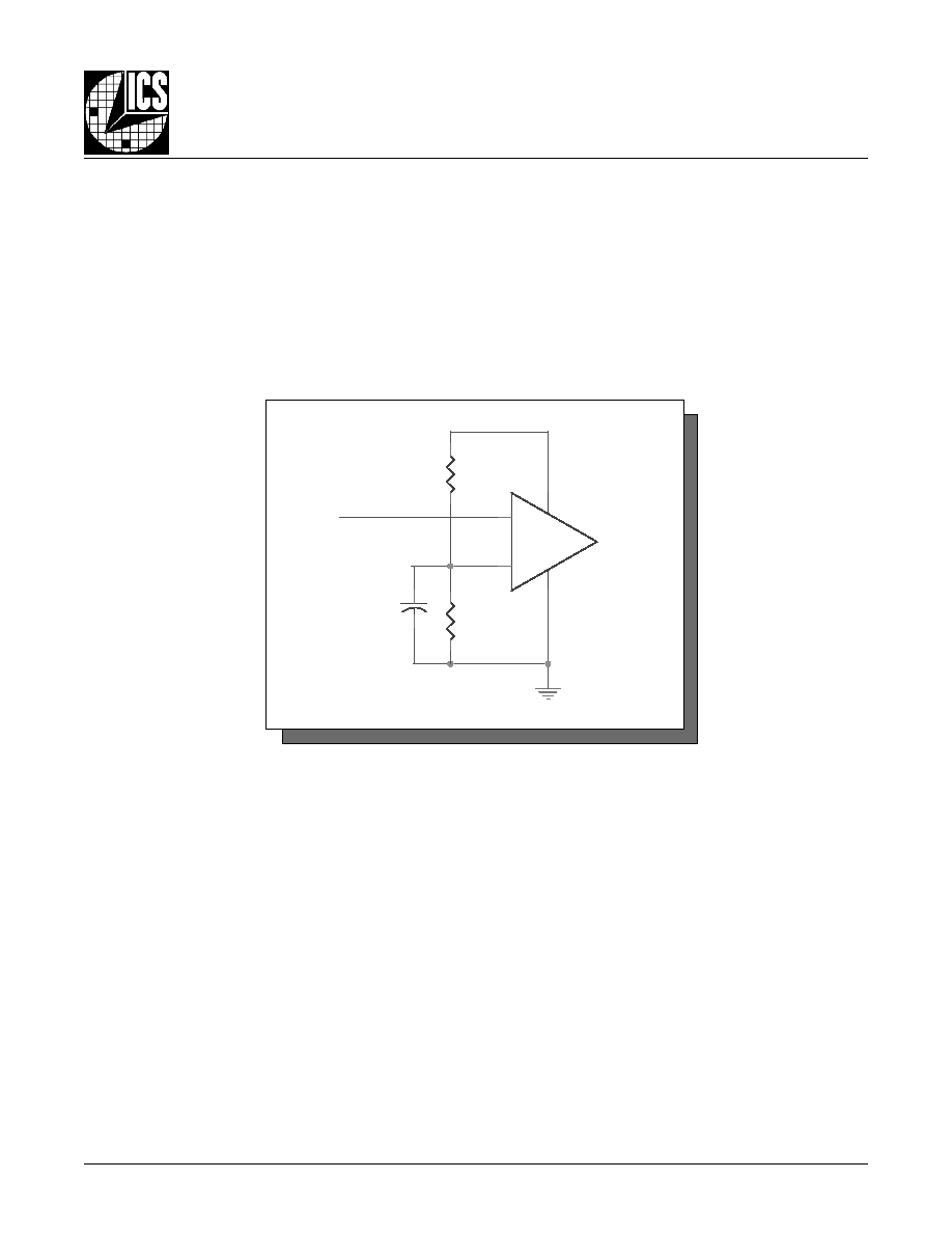
Figure 2 shows how the differential input can be wired to accept
single ended levels. The reference voltage V_REF = V
DD
/2 is
generated by the bias resistors R1, R2 and C1. This bias circuit
should be located as close as possible to the input pin. The ratio
F
IGURE
2. S
INGLE
E
NDED
S
IGNAL
D
RIVING
D
IFFERENTIAL
I
NPUT
R2
1K
V
DD
CLK_IN
+
-
R1
1K
C1
0.1uF
V_REF
of R1 and R2 might need to be adjusted to position the V_REF in
the center of the input voltage swing. For example, if the input
clock swing is only 2.5V and V
DD
= 3.3V, V_REF should be 1.25V
and R2/R1 = 0.609.
W
IRING
THE
D
IFFERENTIAL
I
NPUT
TO
A
CCEPT
S
INGLE
E
NDED
L
EVELS
8523BG
www.icst.com/products/hiperclocks.html
REV. C OCTOBER 25, 2002
8
Integrated
Circuit
Systems, Inc.
ICS8523
L
OW
S
KEW
, 1-
TO
-4
D
IFFERENTIAL
-
TO
-LVHSTL F
ANOUT
B
UFFER
D
IFFERENTIAL
C
LOCK
I
NPUT
I
NTERFACE
The CLK /nCLK accepts LVDS, LVPECL, LVHSTL, SSTL, HCSL
and other differential signals. Both V
SWING
and V
OH
must meet the
V
PP
and V
CMR
input requirements. Figures 4 to 7 show interface
examples for the HiPerClockS CLK/nCLK input driven by the
most common driver types. The input interfaces suggested here
F
IGURE
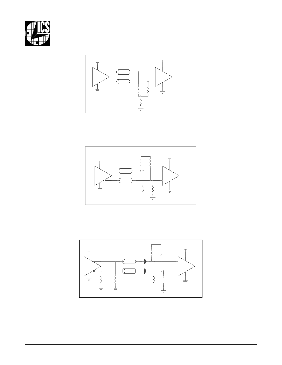
4. H
I
P
ER
C
LOCK
S CLK/
N
CLK I
NPUT
D
RIVEN
BY
ICS H
I
P
ER
C
LOCK
S LVHSTL D
RIVER
are examples only. Please consult with the vendor of the driver
component to confirm the driver termination requirements. For
example in
Figure 4, the input termination applies for ICS
HiPerClockS LVHSTL drivers. If you are using an LVHSTL driver
from another vendor, use their termination recommendation.
S
CHEMATIC
E
XAMPLE
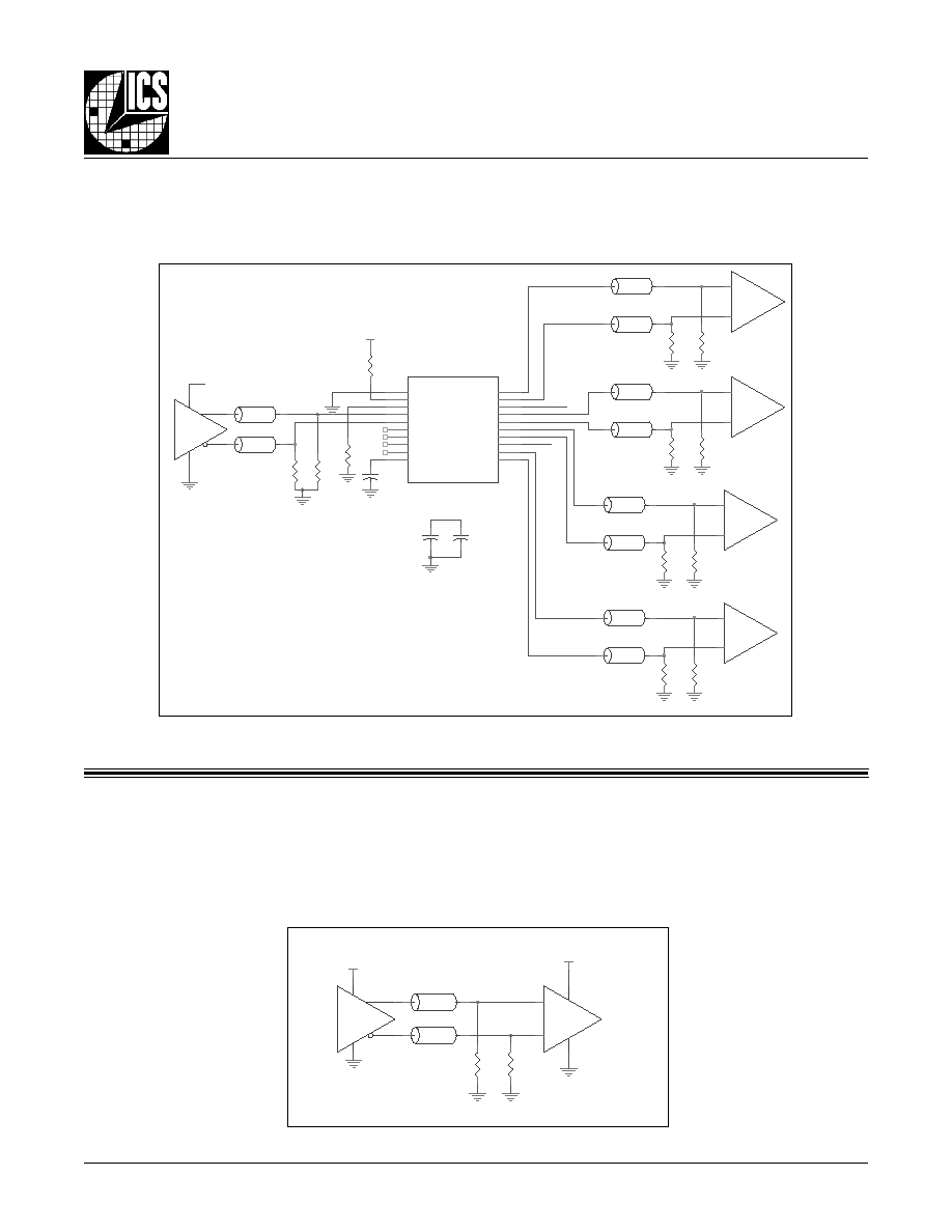
Figure 3 shows a schematic example of the ICS8523. In this
example, the input is driven by an ICS HiPerClockS LVHSTL
driver. The decoupling capacitors should be physically located
1.8V
LVHSTL Driver
Zo = 50
Zo = 50
C2
0.1u
R5
50
R6
50
R10
50
1.8V
R11
1K
R3
50
Zo = 50 Ohm
U3
8523
1
2
3
4
5
6
7
8
9
10
11
12
13
14
15
16
20
19
18
17
GND
CLK_EN
CLK_SEL
CLK
nCLK
PCLK
nPCLK
NC
NC
VDD
nQ3
Q3
VDDO
nQ2
Q2
nQ1
Q0
nQ0
VDDO
Q1
Zo = 50
+
-
Zo = 50 Ohm
Zo = 50
R4
50
R12
1K
R1
50
1.8V
1.8V
+
-
R7
50
R2
50
3.3V
C3
0.1u
R9
50
+
-
Zo = 50
R8
50
+
-
Zo = 50
3.3V
Zo = 50
Zo = 50
C1
0.1u
F
IGURE
3. ICS8523 LVHSTL B
UFFER
S
CHEMATIC
E
XAMPLE
near the power pin. For ICS8523, the unused clock outputs can
be left floating.
1.8V
R2
50
Input
LVHSTL Driver
ICS
HiPerClockS
R1
50
LVHSTL
3.3V
Zo = 50 Ohm
Zo = 50 Ohm
HiPerClockS
CLK
nCLK
8523BG
www.icst.com/products/hiperclocks.html
REV. C OCTOBER 25, 2002
9
Integrated
Circuit
Systems, Inc.
ICS8523
L
OW
S
KEW
, 1-
TO
-4
D
IFFERENTIAL
-
TO
-LVHSTL F
ANOUT
B
UFFER
F
IGURE
6. H
I
P
ER
C
LOCK
S CLK/
N
CLK I
NPUT
D
RIVEN
BY
3.3V LVPECL D
RIVER
F
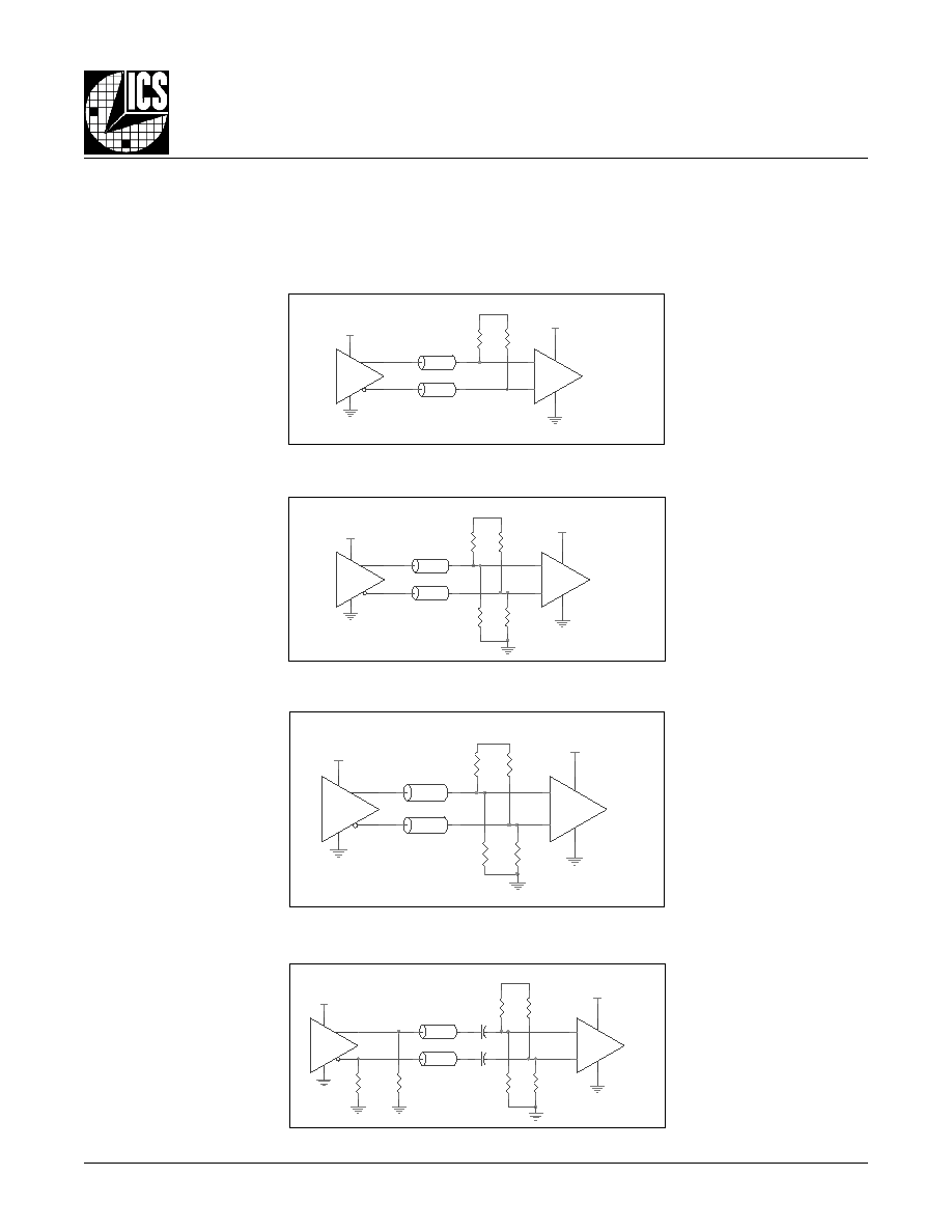
IGURE
5. H
I
P
ER
C
LOCK
S CLK/
N
CLK I
NPUT
D
RIVEN
BY
3.3V LVPECL D
RIVER
F
IGURE
7. H
I
P
ER
C
LOCK
S CLK/
N
CLK I
NPUT
D
RIVEN
BY
3.3V LVPECL D
RIVER
WITH
AC C
OUPLE
3.3V
R1
50
R3
50
Zo = 50 Ohm
LVPECL
Zo = 50 Ohm
HiPerClockS
CLK
nCLK
3.3V
Input
R2
50
Zo = 50 Ohm
Input
HiPerClockS
CLK
nCLK
3.3V
R3
125
R2
84
Zo = 50 Ohm
3.3V
R4
125
LVPECL
R1
84
3.3V
Zo = 50 Ohm
R3
125
HiPerClockS
CLK
nCLK
3.3V
R5
100 - 200
3.3V
R2
84
3.3V
R6
100 - 200
Input
R5,R6 locate near the driver pin.
Zo = 50 Ohm
R1
84
R4
125
C2
LVPECL
C1
8523BG
www.icst.com/products/hiperclocks.html
REV. C OCTOBER 25, 2002
10
Integrated
Circuit
Systems, Inc.
ICS8523
L
OW
S
KEW
, 1-
TO
-4
D
IFFERENTIAL
-
TO
-LVHSTL F
ANOUT
B
UFFER
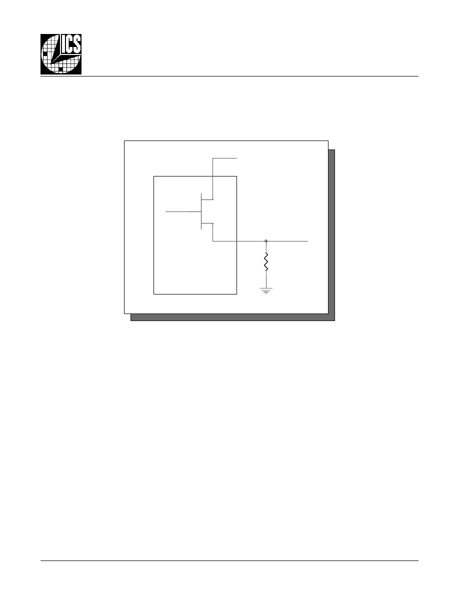
PCLK/nPCLK C
LOCK
I
NPUT
I
NTERFACE
The PCLK /nPCLK accepts LVPECL, CML, SSTL and other differ-
ential signals. Both V
SWING
and V
OH
must meet the V
PP
and V
CMR
input requirements.
Figures 8 to 11 show interface examples for
the HiPerClockS PCLK/nPCLK input driven by the most common
driver types. The input interfaces suggested here are examples
only. If the driver is from another vendor, use their termination rec-
ommendation. Please consult with the vendor of the driver compo-
nent to confirm the driver termination requirements.
F
IGURE
8. H
I
P
ER
C
LOCK
S PCLK/
N
PCLK I
NPUT
D
RIVEN
BY
A
CML D
RIVER
F
IGURE
9. H
I
P
ER
C
LOCK
S PCLK/
N
PCLK I
NPUT
D
RIVEN
BY
AN
SSTL
IN
D
RIVER
F
IGURE
10. H
I
P
ER
C
LOCK
S PCLK/
N
PCLK I
NPUT
D
RIVEN
BY
A
3.3V LVPECL D
RIVER
F
IGURE
11. H
I
P
ER
C
LOCK
S PCLK/
N
PCLK I
NPUT
D
RIVEN
BY
A
3.3V LVPECL D
RIVER
WITH
AC C
OUPLE
HiPerClockS
PCLK
nPCLK
PCLK/nPCLK
3.3V
R2
50
R1
50
3.3V
Zo = 50 Ohm
CML
3.3V
Zo = 50 Ohm
PCLK/nPCLK
2.5V
Zo = 60 Ohm
SSTL
HiPerClockS
PCLK
nPCLK
R2
120
3.3V
R3
120
Zo = 60 Ohm
R1
120
R4
120
2.5V
Zo = 50 Ohm
Input
HiPerClockS
CLK
nCLK
3.3V
R3
125
R2
84
Zo = 50 Ohm
3.3V
R4
125
LVPECL
R1
84
3.3V
3.3V
R5
100 - 200
3.3V
3.3V
HiPerClockS
PCLK
nPCLK
R1
125
PCLK/nPCLK
R2
125
R3
84
C1
C2
Zo = 50 Ohm
R4
84
Zo = 50 Ohm
R6
100 - 200
3.3V LVPECL

8523BG
www.icst.com/products/hiperclocks.html
REV. C OCTOBER 25, 2002
11
Integrated
Circuit
Systems, Inc.
ICS8523
L
OW
S
KEW
, 1-
TO
-4
D
IFFERENTIAL
-
TO
-LVHSTL F
ANOUT
B
UFFER
P
OWER
C
ONSIDERATIONS
This section provides information on power dissipation and junction temperature for the ICS8523.
Equations and example calculations are also provided.
1. Power Dissipation.
The total power dissipation for the ICS8523 is the sum of the core power plus the power dissipated in the load(s).
The following is the power dissipation for V
DD
= 3.3V + 5% = 3.465V, which gives worst case results.
NOTE: Please refer to Section 3 for details on calculating power dissipated in the load.
�
Power (core)
MAX
= V
DD_MAX
* I
DD_MAX
= 3.465V * 50mA = 173.3mW
�
Power (outputs)
MAX
= 32.8mW/Loaded Output pair
If all outputs are loaded, the total power is 4 * 32.8mW = 131.2mW
Total Power
_MAX
(3.465V, with all outputs switching) = 173.3mW + 131.2mW = 305mW
2. Junction Temperature.
Junction temperature, Tj, is the temperature at the junction of the bond wire and bond pad and directly affects the reliability of the
device. The maximum recommended junction temperature for HiPerClockS
TM
devices is 125�C.
The equation for Tj is as follows: Tj =
JA
* Pd_total + T
A
Tj = Junction Temperature
JA
= Junction-to-Ambient Thermal Resistance
Pd_total = Total Device Power Dissipation (example calculation is in section 1 above)
T
A
= Ambient Temperature
In order to calculate junction temperature, the appropriate junction-to-ambient thermal resistance
JA
must be used
. Assuming a
moderate air flow of 200 linear feet per minute and a multi-layer board, the appropriate value is 66.6�C/W per Table 6 below.
Therefore, Tj for an ambient temperature of 70�C with all outputs switching is:
70�C + 0.305W * 66.6�C/W = 90.3�C. This is well below the limit of 125�C
This calculation is only an example. Tj will obviously vary depending on the number of loaded outputs, supply voltage, air flow,
and the type of board (single layer or multi-layer).
q
JA
by Velocity (Linear Feet per Minute)
0
200
500
Single-Layer PCB, JEDEC Standard Test Boards
114.5�C/W
98.0�C/W
88.0�C/W
Multi-Layer PCB, JEDEC Standard Test Boards
73.2�C/W
66.6�C/W
63.5�C/W
NOTE: Most modern PCB designs use multi-layered boards. The data in the second row pertains to most designs.
T
ABLE
6. T
HERMAL
R
ESISTANCE
q
JA
FOR
20-
PIN
TSSOP, F
ORCED
C
ONVECTION
8523BG
www.icst.com/products/hiperclocks.html
REV. C OCTOBER 25, 2002
12
Integrated
Circuit
Systems, Inc.
ICS8523
L
OW
S
KEW
, 1-
TO
-4
D
IFFERENTIAL
-
TO
-LVHSTL F
ANOUT
B
UFFER
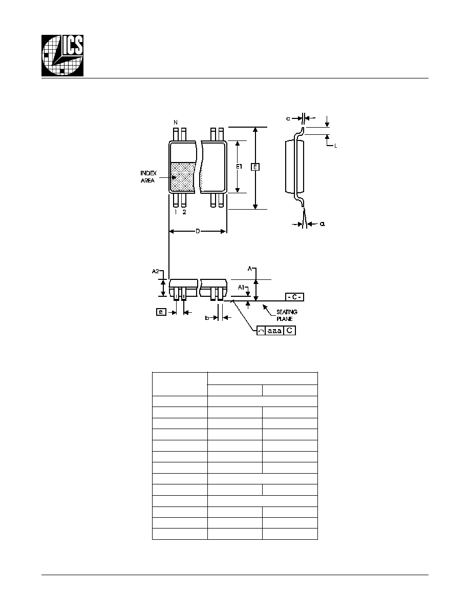
3. Calculations and Equations.
The purpose of this section is to derive the power dissipated into the load.
LVHSTL output driver circuit and termination are shown in
Figure 12.
T
o calculate worst case power dissipation into the load, use the following equations which assume a 50
load.
Pd_H is power dissipation when the output drives high.
Pd_L is the power dissipation when the output drives low.
Pd_H = (V
OH_MIN
/R
L
) * (V
DDO_MAX
- V
OH_MIN
)
Pd_L = (V
OL_MAX
/R
L
) * (V
DDO_MAX
- V
OL_MAX
)
Pd_H = (1V/50
) * (2V - 1V) = 20mW
Pd_L = (0.4V/50
) * (2V - 0.4V) = 12.8mW
Total Power Dissipation per output pair = Pd_H + Pd_L = 32.8mW
F
IGURE
12. LVHSTL D
RIVER
C
IRCUIT
AND
T
ERMINATION
V
DDO
V
OUT
RL
50
Q1

8523BG
www.icst.com/products/hiperclocks.html
REV. C OCTOBER 25, 2002
13
Integrated
Circuit
Systems, Inc.
ICS8523
L
OW
S
KEW
, 1-
TO
-4
D
IFFERENTIAL
-
TO
-LVHSTL F
ANOUT
B
UFFER
R
ELIABILITY
I
NFORMATION
T
RANSISTOR
C
OUNT
The transistor count for ICS8523 is: 472
T
ABLE
7.
JA
VS
. A
IR
F
LOW
T
ABLE
q
JA
by Velocity (Linear Feet per Minute)
0
200
500
Single-Layer PCB, JEDEC Standard Test Boards
114.5�C/W
98.0�C/W
88.0�C/W
Multi-Layer PCB, JEDEC Standard Test Boards
73.2�C/W
66.6�C/W
63.5�C/W
NOTE: Most modern PCB designs use multi-layered boards. The data in the second row pertains to most designs.
8523BG
www.icst.com/products/hiperclocks.html
REV. C OCTOBER 25, 2002
14
Integrated
Circuit
Systems, Inc.
ICS8523
L
OW
S
KEW
, 1-
TO
-4
D
IFFERENTIAL
-
TO
-LVHSTL F
ANOUT
B
UFFER
P
ACKAGE
O
UTLINE
- G S
UFFIX
T
ABLE
8. P
ACKAGE
D
IMENSIONS
Reference Document: JEDEC Publication 95, MS-153
L
O
B
M
Y
S
s
r
e
t
e
m
i
l
l
i
M
m
u
m
i
n
i
M
m
u
m
i
x
a
M
N
0
2
A
-
-
0
2
.
1
1
A
5
0
.
0
5
1
.
0
2
A
0
8
.
0
5
0
.
1
b
9
1
.
0
0
3
.
0
c
9
0
.
0
0
2
.
0
D
0
4
.
6
0
6
.
6
E
C
I
S
A
B
0
4
.
6
1
E
0
3
.
4
0
5
.
4
e
C
I
S
A
B
5
6
.
0
L
5
4
.
0
5
7
.
0
�
0
�
8
a
a
a
-
-
0
1
.
0

8523BG
www.icst.com/products/hiperclocks.html
REV. C OCTOBER 25, 2002
15
Integrated
Circuit
Systems, Inc.
ICS8523
L
OW
S
KEW
, 1-
TO
-4
D
IFFERENTIAL
-
TO
-LVHSTL F
ANOUT
B
UFFER
T
ABLE
9. O
RDERING
I
NFORMATION
While the information presented herein has been checked for both accuracy and reliability, Integrated Circuit Systems, Incorporated (ICS) assumes no responsibility for either its use or for infringement
of any patents or other rights of third parties, which would result from its use. No other circuits, patents, or licenses are implied. This product is intended for use in normal commercial applications.
Any other applications such as those requiring extended temperature range, high reliability, or other extraordinary environmental requirements are not recommended without additional processing by
ICS. ICS reserves the right to change any circuitry or specifications without notice. ICS does not authorize or warrant any ICS product for use in life support devices or critical medical instruments.
r
e
b
m
u
N
r
e
d
r
O
/
t
r
a
P
g
n
i
k
r
a
M
e
g
a
k
c
a
P
t
n
u
o
C
e
r
u
t
a
r
e
p
m
e
T
G
B
3
2
5
8
S
C
I
G
B
3
2
5
8
S
C
I
P
O
S
S
T
d
a
e
l
0
2
e
b
u
t
r
e
p
2
7
C
�
0
7
o
t
C
�
0
T
G
B
3
2
5
8
S
C
I
G
B
3
2
5
8
S
C
I
l
e
e
R
d
n
a
e
p
a
T
n
o
P
O
S
S
T
d
a
e
l
0
2
0
0
5
2
C
�
0
7
o
t
C
�
0
8523BG
www.icst.com/products/hiperclocks.html
REV. C OCTOBER 25, 2002
16
Integrated
Circuit
Systems, Inc.
ICS8523
L
OW
S
KEW
, 1-
TO
-4
D
IFFERENTIAL
-
TO
-LVHSTL F
ANOUT
B
UFFER
T
E
E
H
S
Y
R
O
T
S
I
H
N
O
I
S
I
V
E
R
v
e
R
e
l
b
a
T
e
g
a
P
e
g
n
a
h
C
f
o
n
o
i
t
p
i
r
c
s
e
D
e
t
a
D
B
D
4
T
5
T
5
5
V
d
e
d
d
A
.
e
l
b
a
t
L
T
S
H
V
L
G
N
I
W
S
.
e
l
b
a
T
s
c
i
t
s
i
r
e
t
c
a
r
a
h
C
C
D
L
T
S
H
V
L
o
t
w
o
r
t
.
e
l
b
a
t
s
c
i
t
s
i
r
e
t
c
a
r
a
h
C
C
A
D
P
;
.
n
i
M
o
t
3
.
1
f
o
e
u
l
a
v
d
e
d
d
a
,
w
o
r
.
6
.
1
o
t
0
.
2
m
o
r
f
.
x
a
M
d
e
g
n
a
h
c
1
0
/
1
3
/
7
B
3
.
m
a
r
g
a
i
D
g
n
i
m
i
T
N
E
_
K
L
C
,
1
e
r
u
g
i
F
d
e
t
a
d
p
U
1
0
/
7
1
/
0
1
B
3
.
m
a
r
g
a
i
D
g
n
i
m
i
T
N
E
_
K
L
C
,
1
e
r
u
g
i
F
d
e
t
a
d
p
U
1
0
/
2
/
1
1
C
5
T
5
.
e
l
b
a
t
s
c
i
t
s
i
r
e
t
c
a
r
a
h
C
C
A
t
D
P
.
s
n
0
.
1
o
t
s
n
3
.
1
m
o
r
f
.
n
i
M
d
e
g
n
a
h
c
,
w
o
r
.
s
p
0
0
2
o
t
s
p
0
5
1
m
o
r
f
.
x
a
M
d
e
g
n
a
h
c
,
w
o
r
)
p
p
(
k
s
t
2
0
/
1
1
/
1
C
1
V
8
.
1
t
u
o
k
o
o
t
-
6
,
1
t
e
ll
u
B
,
n
o
i
t
c
e
s
s
e
r
u
t
a
e
F
d
e
s
i
v
e
R
2
0
/
6
/
5
C
0
1
-
8
s
e
l
p
m
a
x
E
c
i
t
a
m
e
h
c
S
d
e
d
d
a
,
n
o
i
t
c
e
s
n
o
i
t
a
m
r
o
f
n
I
n
o
i
t
a
c
il
p
p
A
e
h
t
n
I
2
0
/
5
2
/
0
1
Document Outline
- General Description
- Features
- Block Diagram
- Pin Assignment
- Pin Descriptions
- Pin Characteristics
- Control Input Function Table
- CLK_EN Timing Diagram
- Clock Input Function Table
- Absolute Maximum Ratings
- Power Supply DC Characteristics
- LVCMOS DC Characteristics
- Differential DC Characteristics
- LVPECL DC Characteristics
- LVHSTL DC Characteristics
- AC Characteristics
- Parameter Measurement Information
- 3.3V/1.8V Output Load AC Test Circuit Diagram
- Differential Input Level Diagram
- Output Skew Diagram
- Part-to-Part Skew Diagram
- Output Rise/Fall Time Diagram
- Propagation Delay Diagram
- odc & tPeriod Diagram
- Application Information
- Wiring the Differential Input to Accept Single Ended Levels
- Single Ended Signal Driving Differential Input
- Schematic Example
- Differential Clock Input Interface
- HiPerClockS CLK/nCLK Input Driven by ICS HiPerClockS LVHST Driver Diagram
- HiPerClockS CLK/nCLK Input Driven by 3.3V LVPECL Driver Diagram
- HiPerClockS CLK/nCLK Input Driven by 3.3V LVPECL Driver Diagram
- HiPerClockS CLK/nCLK Input Driven by 3.3V LVPECL Driver with AC Couple Diagram
- PCLK/nPCLK Clock Input Interface
- HiPerClockS PCLK/nPCLK Input Driven by a CML Driver Diagram
- HiPerClockS PCLK/nPCLK Input Driven by an SSTL in Driver Diagram
- HiPerClockS PCLK/nPCLK Input Driven by a 3.3V LVPECL Driver Diagram
- HiPerClockS PCLK/nPCLK Input Driven by a 3.3V LVPECL Driver with AC Couple Diagram
- Power Considerations
- Power Dissipation
- Junction Temperature
- Thermal Resistance
- Calculations & Equations
- LVHSTL Driver Circuit & Termination Diagram
- Reliability Information
- Transistor Count
- Package Outline
- Package Dimensions
- Ordering Information