Integrated
Circuit
Systems, Inc.
General Description
Features
AV9173 -15
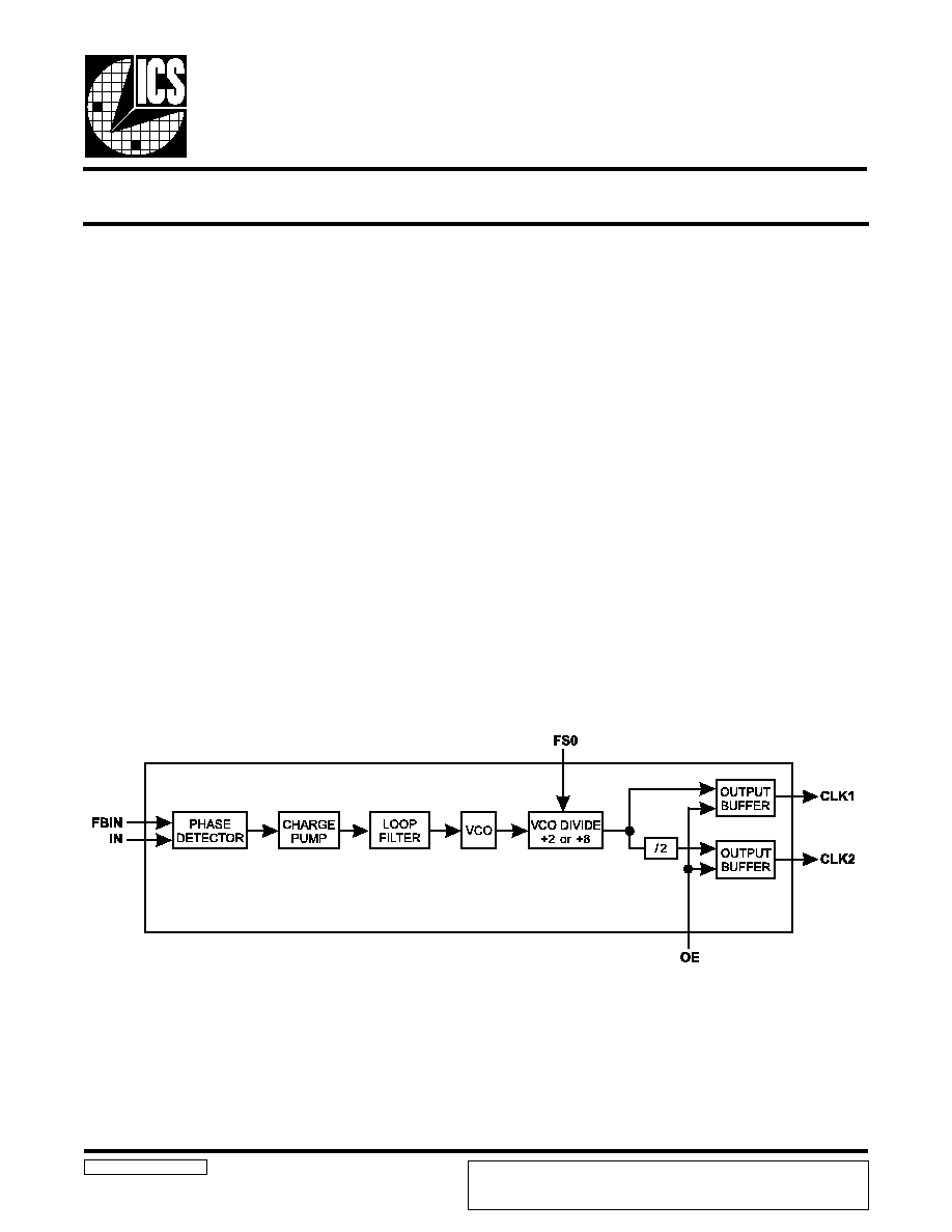
Block Diagram
Video Genlock PLL
AV9173-15RevC051397P
∑
Phase-detector/VCO circuit block
∑
Ideal for genlock system
∑
Reference clock range 12 kHz to 1 MHz
(see specification of output clock range)
∑
Output clock range 0.625 to 37.5 MHz for CLK1,
depending on input conditions (see Table 1) on page 2.
∑
Provides h-sync capability with CLK1 outputs
15 to 37.5 MHz for 15 kHz input
∑
On-chip loop filter
∑
Single 5 volt power supply
∑
Low power CMOS technology
∑
Small 8-pin DIP or SOIC package
The AV9173-15 provides the analog circuit blocks required
for implementing a video genlock dot (pixel) clock
generator. It contains a phase detector, charge pump, loop
filter, and voltage-controlled oscillator (VCO). By grouping
these critical analog blocks into one IC and utilizing
external digital functions, performance and design
flexibility are optimized as are development time and
system cost.
When used with an external clock divider, the AV9173-15
forms a Phase-Locked Loop configured as a frequency
synthesizer. The AV9173-15 is designed to accept video
horizontal synchronization (h-sync) pulses and produce a
video dot clock. A separated, negative-going sync input
reference pulse is required at pin 2 (I N).
The AV9173-15 is also suited for other clock recovery
applications in such areas as data communications.
ICS reserves the right to make changes in the device data identified in this
publication without further notice. ICS advises its customers to obtain the latest
version of all device data to verify that any information being relied upon by the
customer is current and accurate.

2
AV9173-15
Pin Descriptions
Pin Configuration
8-Pin DIP or SOIC
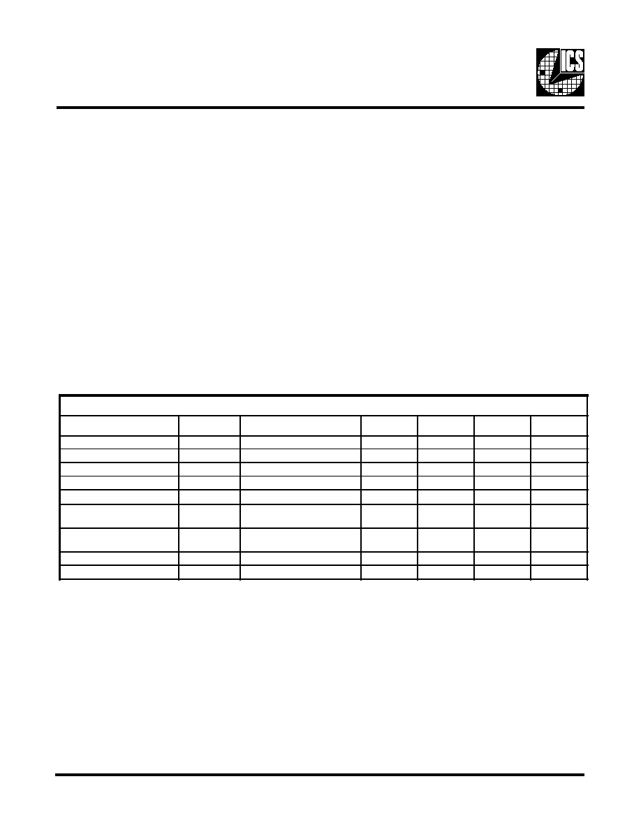
Table 1: Allowable Input Frequency to Output Frequency
(Outputs in MHz)
PIN
NUMBER
PIN NAME
TYPE
DESCRIPTION
1
FBIN
Input
Feedback Input
2
IN
Input
Input for reference sync pulse
3
GND
--
Ground
4
FS0
Input
Internal VCO divider select input
5
OE
Input
Output Enable
6
CLK1
Output
Clock Output 1
7
VDD
--
Power Supply (+5V)
8
CLK2
Output
Clock Output 2 (Divided-by-2 from Clock 1)
f
IN
(kHz)
f
OUT
for FS = 0 (MHz)
f
OUT
for FS = 1 (MHz)
CLK1 Output
CLK2 Output
CLK1 Output
CLK2 Output
12
f
IN
14 kHz
22.0 to 37.5
11.0 to 18.75
5.5 to 9.375
2.75 to 4.6875
14
<
f
IN
17 kHz
15 to 37.5
7.5 to 18.75
3.75 to 9.375
1.875 to 4.6875
17
<
f
IN
30 kHz
12.5 to 37.5
6.25 to 18.75
3.125 to 9.375
1.5625 to 4.6875
30
<
f
IN
35 kHz
7.5 to 37.5
3.75 to 18.75
1.875 to 9.375
0.9375 to 4.6875
35
<
f
IN
1000 kHz
5.0 to 37.5
2.5 to 18.75
1.25 to 9.375
0.625 to 4.6875

3
AV9173 -15
Using the AV9173- 15
Figure 1: Typical Application of AV9173-15 in a Video Genlock System
Most video sources, such as video cameras, are asynchronous,
free-running devices. To digitize video or synchronize one
video source to another free-running reference video source, a
video "genlock" (generator lock) circuit is required. The
AV9173-15 integrates the analog blocks which make the task
much easier.
In the complete video genlock circuit, the primary function of
the AV9173-15 is to provide the analog circuitry required to
generate the video dot clock within a PLL. This application is
illustrated in Figure 1. The input reference signal for this
circuit is the horizontal synchronization (h-sync) signal. If a
composite video reference source is being used, the h-sync
pulses must be separated from the composite signal. A video
sync separator circuit, such as the National Semiconductor
LM1881, can be used for this purpose.
The clock feedback divider shown in Figure 1 is a digital
divider used within the PLL to multiply the reference
frequency. Its divide ratio establishes how many video dot
clock cycles occur per h-sync pulse. For example, if 880 pixel
clocks are desired per h-sync pulse, then the divider ratio is set
to 880. Hence, together the h-sync frequency and external
divider ratio establish the dot clock frequency:
f
OUT
=
f
IN
∑ N where N is external divide ratio
Both AV9173-15 input pins IN and FBIN respond only to
negative-going clock edges of the input signal. The h-sync
signal must be constant frequency in the 12 k Hz to 1 MHz
range and stable (low clock jitter) for creation of a stable
output clock.
The output hook-up of the AV9173-15 is dictated by the
desired dot clock frequency. The primary consideration is the
internal VCO which operates over a frequency range of
10 MHz to 75 MHz. Because of the selectable VCO output
divider and the additional divider on output CLK2, four
distinct output frequency ranges can be achieved. The
following Table lists these ranges and the corresponding
device configuration.
Note that both outputs, CLK1 and CLK2, are available during
operation even though only one is fed back via the external
clock divider.
Pin 5, OE, tristates both CLK1 and CLK2 upon logic low
input. This feature can be used to revert dot clock control to
the system clock when not in genlock mode (hence, when in
genlock mode the system dot clock must be tristated).
When unused, inputs FS0 and OE must be tied to either GND
(logic low) or VDD (logic high).
For further discussion of VCO/PLL operation as it applies to
the AV9173-15, please refer to the AV9170 application note.
The AV9170 is a similar device with fixed feedback dividers
for skew control applications.
FS0 State
Output Used
Frequency Range
0
0
1
1
CLK1
CLK2
CLK1
CLK2
5 - 37.5 MHz
2.5 - 18.75 MHz
1.25 - 9.375 MHz
0.625 - 4.6875 MHz
4
AV9173-15
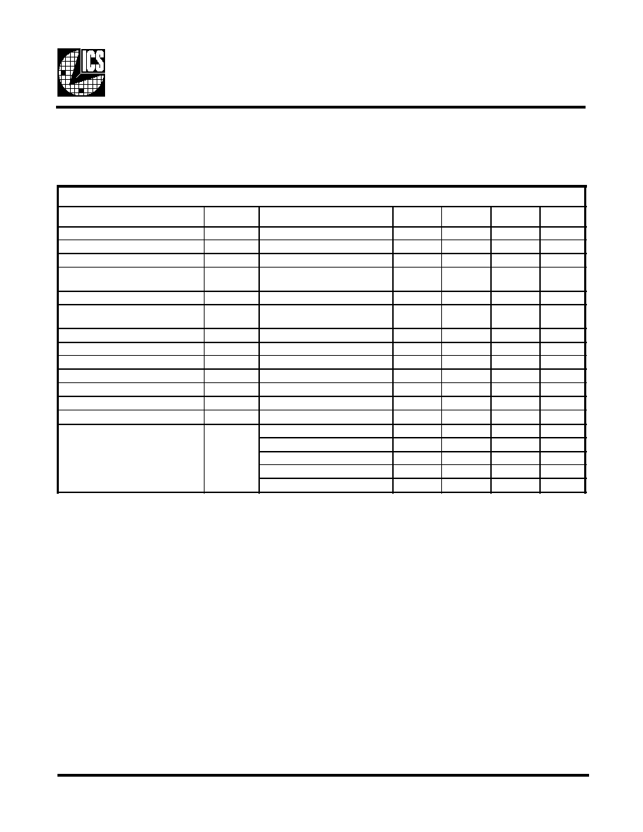
Absolute Maximum Ratings
V
DD
(referenced to GND) . . . . . . . . . . . . . . . . 7.0 V
Operating Temperature under Bias . . . . . . . . . 0∞ C to +70∞ C
Storage Temperature . . . . . . . . . . . . . . . . . . . . ≠ 65∞C to +150∞C
Voltage on I/O pins referenced to GND . . . . . GND ≠ 0.5 V to V
DD
+ 0.5 V
Power Dissipation . . . . . . . . . . . . . . . . . . . . . . 0.5 watts
Stresses above those listed under Absolute Maximum Ratings above may cause permanent damage to the device. This is a stress
rating only and functional operation of the device at these or any other conditions above those listed in the operational sections
of the specifications is not implied. Exposure to absolute maximum rating conditions for extended periods may affect product
reliability.
V
DD
= +5V ±5%, T
A
= 0∞C to 70∞C, unless otherwise stated
Electrical Characteristic
Notes:
1. Parameter is guaranteed by design and characterization. Not 100% tested in production.
DC CHARACTERISTICS
PARAMETER
SYMBOL
TEST CONDITIONS
MIN
TYP
MAX
UNITS
Input Low Voltage
V
IL
V
DD
= 5V
--
--
0.8
V
Input High Voltage
V
IH
V
DD
= 5V
2.0
--
--
V
Input Low Current
I
IL
V
IN
= 0V
-
5
--
--
µ A
Input High Current
I
IH
V
IN
= V
DD
-
5
--
5
µ A
Output Low Voltage
1
V
OL
I
O L
= 8mA
--
--
0.4
V
Output High Voltage
1
V
OH1
I
O H
= -1mA,
V
DD
= 5.0V
V
DD
-.4V
--
--
V
Output High Voltage
1
V
OH2
I
O H
= -4mA,
V
DD
= 5.0V
V
DD
-.8V
--
--
V
Output High Voltage
1
V
OH3
I
O H
= -8mA
2.4
--
--
V
Supply Current
I
DD
Unloaded, 50 MHZ
--
20
50
mA
5
AV9173 -15
V
DD
= +5V ±5%, T
A
= 0∞C to 70∞C, unless otherwise stated
Electrical Characteristics
Notes:
1. Parameter is guaranteed by design and characterization. Not 100% tested in production.
2. Input Reference Frequency = 25 kHz, Output Frequency = 25 MHz. Jitter measured between adjacent vertical pixels.
3. CLK1 frequency applies for FS = 0. For FS = 1 condition, divide allowable CLK1 range by the factor of 4.
AC CHARACTERISTICS
PARAMETER
SYMBOL
TEST CONDITIONS
MIN
TYP
MAX
UNITS
Input Clock Rise Time
1
ICLK
r
--
--
10
ns
Input Clock Fall Time
1
ICLK
f
--
--
10
ns
Output Rise Time
1
t
r 1
15pF load; 0.8 to 2.0V
--
0.6
1.5
ns
Rise time
1
t
r 2
15pF load;
20% to 80% V
DD
--
1.3
3.0
ns
Output Fall time
1
t
f 1
15pF load; 2.0 to 0.8V
--
0.6
1.5
ns
Fall time
1
t
f 2
15pF load;
80% to 20% V
DD
--
0.7
2.0
ns
Output Duty Cycle
1
d
t
15pF load, V
T H
=1.4V
40
47
55
%
Jitter,
1
1 sigma
T
1s1
CLK1 freq.
12.5 MHz
--
120
250
ps
Jitter,
1
1 sigma
T
1s2
CLK1 freq.
12.5 MHz
--
--
1
%
Jitter,
1
1 absolute
T
abs 1
CLK1 freq.
<
12.5 MHz
-400
±250
400
ps
Jitter,
1
1 absolute
T
abs 2
CLK1 freq.
<
12.5 MHz
--
--
2
%
Line-to-line jitter,
1
absolute
2
TL
abs
--
±4
--
ns
Input Frequency,
1
IN or FBIN
f
i 1
f
VCO
10 to 75 MHz
12.0
--
1000
kHz
CLK1 Frequency
3
f
CLK1
12
f
i
14 kHz
22.0
--
37.5
MHz
14
<
f
i
17 kHz
15.0
--
37.5
MHz
17
<
f
i
30 kHz
12.5
--
37.5
MHz
30
<
f
i
35 kHz
7.5
--
37.5
MHz
35
<
f
i
1000 kHz
5.0
--
37.5
MHz

6
AV9173-15
Ordering Information
AV9173-15CN08 - or - AV9173-15CS08
8-Pin DIP PACKAGE
8-Pin SOIC PACKAGE
XXX XXXX - PPP M X#W
Lead Count & Package Width
Lead Count = 1, 2 or 3 digits
W = 0.3" SOIC or 0.6" DIP; None = Standard Width
Package Type
N = DIP (Plastic)
S = SOIC
Pattern Number (2 or 3 digit number for parts with ROM code patterns)
Device Type (consists of 3 or 4 digit numbers)
Prefix
ICS, AV = Standard Device
Example:
PRODUCT PREVIEW documents contain information on products in the formative or
design phase development. Charactersitic data and other specifications are design goals.
ICS reserves the right to change or discontinue these procucts without notice.