
Philips
Semiconductors
CBT16212
24-bit bus exchange switch
with 12-bit output enables
Product data
File under Integrated Ciruits ICL03
2001 Sep 28
INTEGRATED CIRCUITS

Philips Semiconductors
Product data
CBT16212
24-bit bus exchange switch with 12-bit output enables
2
2001 Sep 28
853≠2283 27173
FEATURES
∑
5
switch connection between two ports
∑
TTL compatible control input levels
∑
Latch-up testing is done to JEDEC Standard JESD78 which
exceeds 100 mA
∑
ESD protection exceeds 1500 V HBM per JESD22-A114 and
1000 V CDM per JESD22-C101
DESCRIPTION
The CBT16212 provides 24 bits of high-speed TTL-compatible bus
switching or exchanging. The low on-state resistance of the switch
allows connections to be made with minimal propagation delay.
The CBT16212 operates as 24-bit bus switch or a 12-bit bus
exchanger, which provides data exchanging between the four signal
ports via the data-select (S0≠S2) terminals.
The CBT16212 is characterized for operation from ≠40 to +85
∞
C.
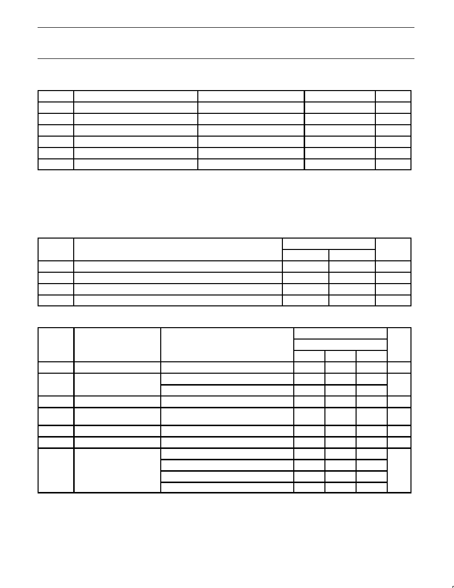
QUICK REFERENCE DATA
SYMBOL
PARAMETER
CONDITIONS
T
amb
= 25
∞
C; GND = 0 V
TYPICAL
UNIT
t
pd
Propagation delay
An to Bn
C
L
= 50 pF; V
CC
= 5 V
0.25
ns
C
IN
Input capacitance
V
I
= 0 V or V
CC
4.5
pF
C
OUT
Output capacitance
Outputs disabled; V
O
= 0 V or V
CC
11.5
pF
r
on
A1 to A2
V
CC
= 4.5 V; V
I
= 0 V
4
ORDERING INFORMATION
PACKAGES
TEMPERATURE RANGE
ORDER CODE
DRAWING NUMBER
56-Pin Plastic SSOP
≠40 to +85
∞
C
CBT16212DL
SOT371-1
56-Pin Plastic TSSOP
≠40 to +85
∞
C
CBT16212DGG
SOT364-1
NOTE:
1. Standard packing quantities and other packaging data is available at www.philipslogic.com/support/packages.
FUNCTION TABLE
S2
S1
S0
A1
A2
FUNCTION
L
L
L
Z
Z
Disconnect
L
L
H
B1
Z
A1 = B1
L
H
L
B2
Z
A1 = B2
L
H
H
Z
B1
A2 = B1
H
L
L
Z
B2
A2 = B2
H
L
H
Z
Z
Disconnect
H
H
L
B1
B2
A1 = B1, A2 = B2
H
H
H
B2
B1
A1 = B2, A2 = B1
H = High voltage level
L
= Low voltage level
Z = High impedance "off " state
LOGIC SYMBOL
FLOW CONTROL
SA00512
1 of 12 Channels
2
54
3
53
1
56
55
1A1
1A2
S0
S1
S2
1B1
1B2

Philips Semiconductors
Product data
CBT16212
24-bit bus exchange switch with 12-bit output enables
2001 Sep 28
3
PIN CONFIGURATION
1
2
3
4
5
6
7
8
9
10
11
12
13
14
15
16
17
18
19
20
33
34
35
36
37
38
39
40
41
42
43
44
45
46
47
48
21
22
23
24
49
50
51
52
53
54
55
56
25
26
27
28
32
31
30
29
S0
1A1
1A2
2A1
2A2
3A1
3A2
GND
4A1
4A2
5A1
5A2
6A1
6A2
7A1
7A2
V
CC
8A1
GND
8A2
9A1
9A2
10A1
10A2
11A1
11A2
12A1
12A2
S1
S2
1B1
1B2
2B1
2B2
3B1
GND
3B2
4B1
4B2
5B1
5B2
6B1
6B2
7B1
7B2
8B1
GND
8B2
9B1
9B2
10B1
10B2
11B1
11B2
12B1
12B2
SA00511
PIN DESCRIPTION
PIN NUMBER
SYMBOL
NAME AND FUNCTION
1, 56, 55
S0, S1, S2
Data select
2, 4, 6, 9, 11, 13, 15,
18, 21, 23, 25, 27
1A1≠12A1
A1 channel
3, 5, 7, 10, 12, 14, 16,
20, 22, 24, 26, 28
1A2≠12A2
A2 channel
54, 52, 50, 47, 45, 43,
41, 39, 36, 34, 32, 30
1B1, 12B1
B1 channel
53, 51, 48, 46, 44, 42,
40, 37, 35, 33, 31, 29
1B2, 12B2
B2 channel
8, 19, 38, 49
GND
Ground (0 V)
17
V
CC
Positive supply voltage
Philips Semiconductors
Product data
CBT16212
24-bit bus exchange switch with 12-bit output enables
2001 Sep 28
4
ABSOLUTE MAXIMUM RATINGS
1, 2
SYMBOL
PARAMETER
CONDITIONS
RATING
UNIT
V
CC
DC supply voltage
≠0.5 to +7.0
V
I
IK
DC input diode current
V
I
< 0
≠50
mA
V
I
DC input voltage
3
≠0.5 to +7.0
V
V
OUT
DC output voltage
3
output in Off or High state
≠0.5 to +5.5
V
I
OUT
DC output current
output in Low state
128
mA
T
stg
Storage temperature range
≠65 to 150
∞
C
NOTES:
1. Stresses beyond those listed may cause permanent damage to the device. These are stress ratings only and functional operation of the
device at these or any other conditions beyond those indicated under "recommended operating conditions" is not implied. Exposure to
absolute-maximum-rated conditions for extended periods may affect device reliability.
2. The performance capability of a high-performance integrated circuit in conjunction with its thermal environment can create junction
temperatures which are detrimental to reliability. The maximum junction temperature of this integrated circuit should not exceed 150
∞
C.
3. The input and output voltage ratings may be exceeded if the input and output current ratings are observed.
RECOMMENDED OPERATING CONDITIONS
SYMBOL
PARAMETER
LIMITS
UNIT
SYMBOL
PARAMETER
Min
Max
UNIT
V
CC
DC supply voltage
4.0
5.5
V
V
IH
High-level input voltage
2.0
--
V
V
IL
Low-level Input voltage
--
0.8
V
T
amb
Operating free-air temperature range
≠40
+85
∞
C
DC ELECTRICAL CHARACTERISTICS
LIMITS
SYMBOL
PARAMETER
TEST CONDITIONS
T
amb
= ≠40 to +85
∞
C
UNIT
Min
Typ
1
Max
V
IK
Input clamp voltage
V
CC
= 4.5 V; I
I
= ≠18 mA
--
--
≠1.2
V
I
Input leakage current
V
CC
= 0 V; V
I
= 5.5 V
--
--
10
µ
A
I
I
Input leakage current
V
CC
= 5.5 V; V
I
= GND or 5.5 V
--
--
±
1
µ
A
I
CC
Quiescent supply current
V
CC
= 5.5 V; I
O
= 0, V
I
= V
CC
or GND
--
--
3
µ
A
I
CC
Additional supply current per
input pin
2
V
CC
= 5.5 V, one input at 3.4 V,
other inputs at V
CC
or GND
--
--
2.5
mA
C
I
Control pins capacitance
V
I
= 3 V or 0
--
4.7
--
pF
C
IO(OFF)
Port Off capacitance
V
O
= 3 V or 0; S0, S1, or S2 = V
CC
--
11.5
--
pF
3
V
CC
= 4.0 V; V
1
= 2.4 V; I
I
= 15 mA
--
--
21
r
3
A1 to A2
V
CC
= 4.5 V; V
1
= 0 V; I
I
= 64 mA
--
4
7
r
on
3
A1 to A2
V
CC
= 4.5 V; V
1
= 0 V; I
I
= 30 mA
--
4
7
V
CC
= 4.5 V; V
1
= 2.4 V; I
I
= 15 mA
--
6
12
NOTES:
1. All typical values are at V
CC
= 5 V, T
amb
= 25
∞
C
2. This is the increase in supply current for each input that is at the specified TTL voltage level rather than V
CC
or GND.
3. Measured by the voltage drop between the A and the B terminals at the indicated current through the switch.
On-state resistance is determined by the lowest voltage of the two (A or B) terminals.

Philips Semiconductors
Product data
CBT16212
24-bit bus exchange switch with 12-bit output enables
2001 Sep 28
5
AC CHARACTERISTICS
GND = 0 V; t
R;
C
L
= 50 pF
SYMBOL
PARAMETER
FROM (INPUT)
TO
V
CC
= 5.0 V
±
0.5 V
UNIT
SYMBOL
PARAMETER
FROM (INPUT)
(OUTPUT)
Min
Max
UNIT
t
Propagation delay
1
A or B
B or A
0 25
ns
t
pd
Propagation delay
1
A or B
B or A
--
0.25
ns
t
en
Output enable time
to High and Low level
S
A or B
3.6
8.0
ns
t
dis
Output disable time
from High and Low level
S
A or B
4.3
8.0
ns
NOTES:
1. This parameter is warranted but not production tested. The propagation delay is based on the RC time constant of the typical on-state
resistance of the switch and a load capacitance of 50 pF, when driven by an ideal voltage source (zero output impedance).
AC WAVEFORMS
V
M
= 1.5 V, V
IN
= GND to 3.0 V
INPUT
1.5 V
OUTPUT
t
PLH
t
PHL
SA00028
1.5 V
1.5 V
1.5 V
3 V
0 V
V
OH
V
OL
Waveform 1. Input (An) to Output (Yn) Propagation Delays
Output Control
(Low-level
enabling )
1.5 V
t
PZH
t
PHZ
V
OH
V
OL
t
PZL
t
PLZ
3.5 V
0 V
V
OL
+ 0.3 V
V
OH
≠ 0.3 V
SA00029
1.5 V
1.5 V
1.5 V
0 V
3 V
Output
Waveform 1
S1 at 7 V
(see Note)
Note:
Waveform 1 is for an output with internal conditions such that
the output is low except when disabled by the output control.
Waveform 2 is for an output with internal conditions such that
the output is high except when disabled by the output control.
Output
Waveform 2
S1 at Open
(see Note)
Waveform 2. 3-State Output Enable and Disable Times
TEST CIRCUIT AND WAVEFORMS
C
L
= 50 pF
500
Load Circuit
DEFINITIONS
C
L
=
Load capacitance includes jig and probe capacitance;
see AC CHARACTERISTICS for value.
TEST
S1
t
pd
open
t
PLZ
/t
PZL
7 V
t
PHZ
/t
PZH
open
SA00012
500
From Output
Under Test
S1
7 V
Open
GND