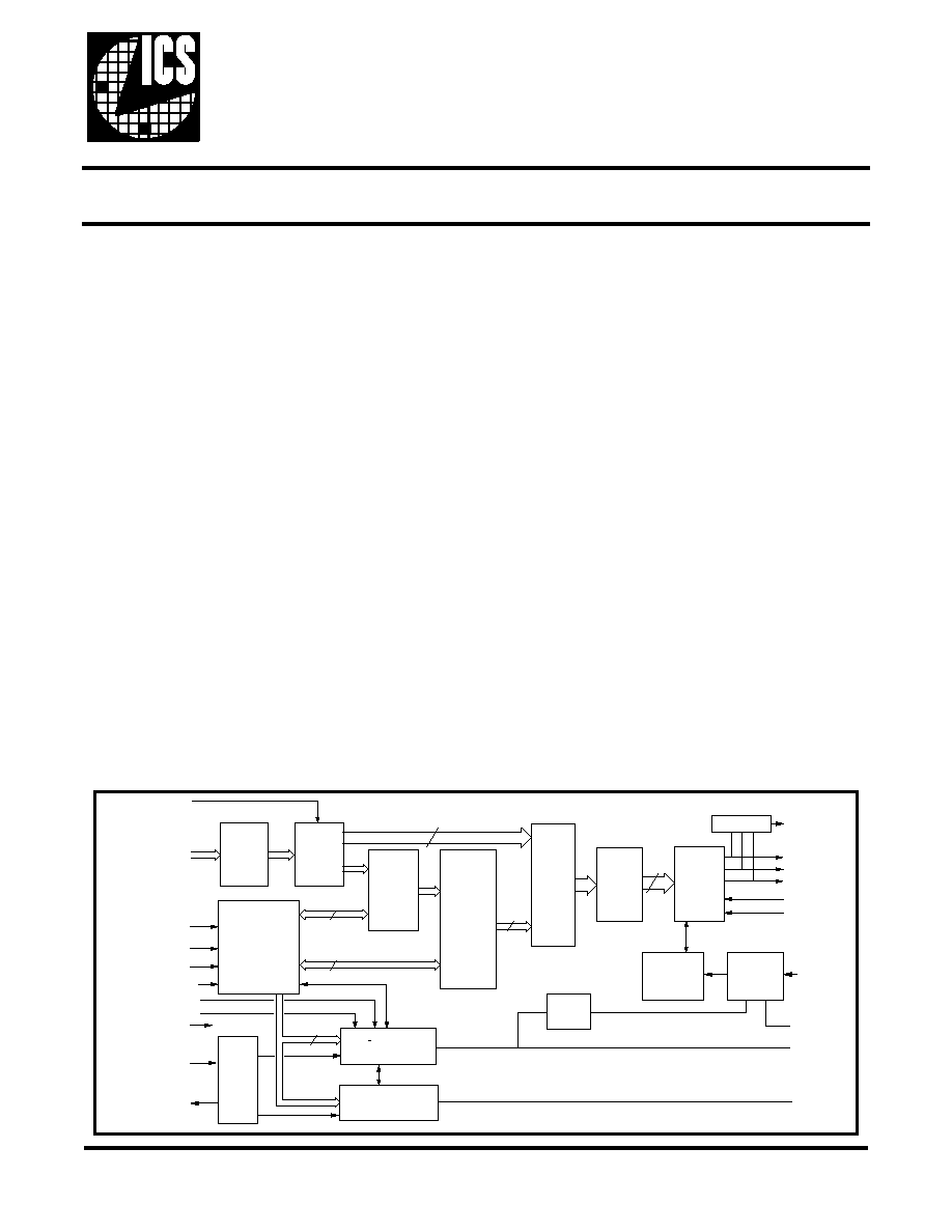
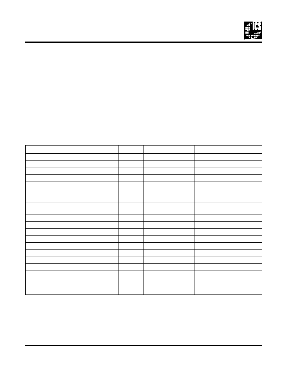
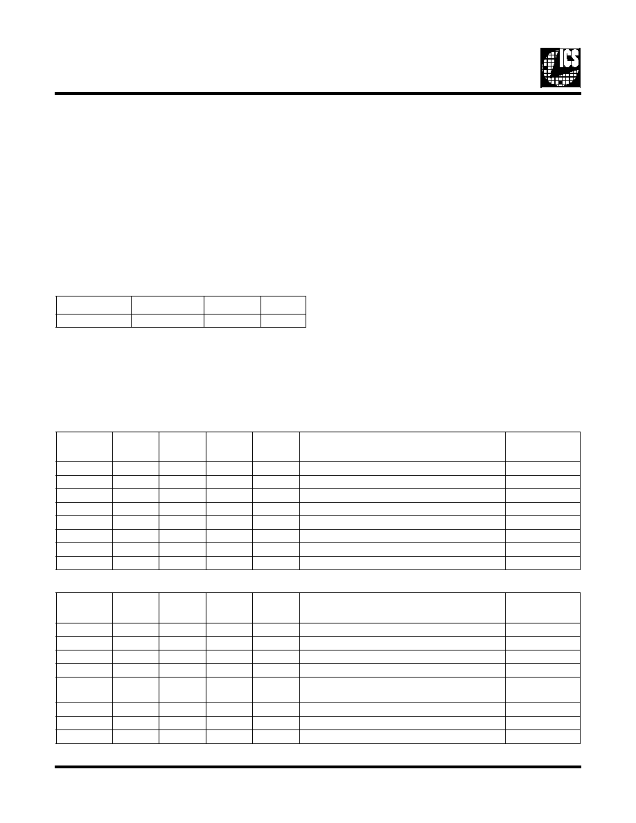
Block Schematic
PIXEL
ADR
AND
MASK
COLOR
PALETTE
256 x 18
BIT
24
18
BYPS
MUX
NORM
LATCH
24
COMPARE
TRIPLE
6/8-BIT
DAC
TIMING
GEN.
MUX.
MODE
CTL
8 PLL
PARAMETER &
CLK0 PLL
1 PLL
PARAMETER &
CLK1 PLL
2X
CLK0
CLK1
RED
GREEN
BLUE
RSET
VREF
BUFF.
LATCH
MICRO-
PROCESSOR
INTERFACE
XTAL
OSC
8
16
16
BLANK*
PCLK
P0-P15
D0-D7
WR*
RD*
RS0-RS2
XIN
XOUT
STROBE
CS0-CS2
PCLK
SENSE*
5342_01.ai
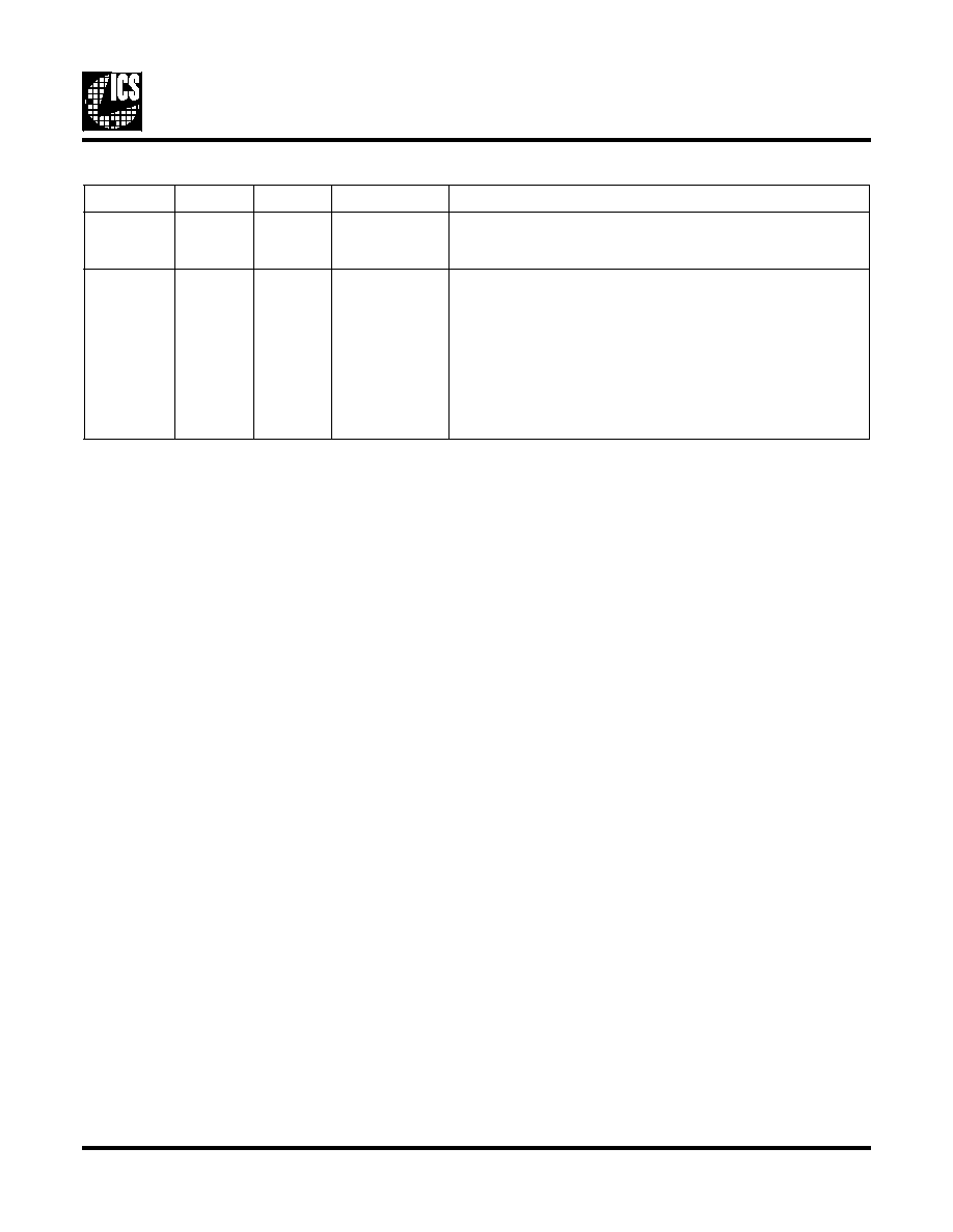
General Description
The ICS5342 GENDAC is a combination of dual programma-
ble clock generators, a 256 x 18-bit RAM, and a triple 8-bit
video DAC. The GENDAC supports 8-bit pseudo color appli-
cations, as well as 15-bit, 16-bit, and 24-bit True Color bypass
for high speed, direct access to the DACs.
The RAM makes it possible to display 256 colors selected
from a possible 262,144 colors. The dual clock generators use
Phase Locked Loop (PLL) technology to provide program-
mable frequencies for use in the graphics subsystem. The vid-
eo clock contains 8 frequencies, all of which are
programmable by the user. The memory clock has two pro-
grammable frequency locations.
The three 8-bit DACs on the ICS5342 are capable of driving
singly or doubly-terminated 75
loads to nominal 0 - 0.7
volts at pixel rates up to 135 MHz. Differential and integral
linearity errors are less than 1 LSB over full temperature and
VDD ranges. Monotonicity is guaranteed by design. On-chip
pixel mask register allows displayed colors to be changed in
a single write cycle rather than by modifying the color palette.
ICS is the world leader in all aspects of frequency (clock) gen-
eration for graphics, using patented techniques to produce
low jitter video timing.
Features
�
Triple video DAC, dual clock generator, and 16 bit pixel
port
�
Dynamic mode switch allows switching of color depth
on a pixel by pixel basis
�
24 (packed and sparse), 16, 15, or 8-bit pseudo color
pixel mode supports True Color, Hi-Color, and VGA
modes
�
High speed 256 x 6 x 3 color palette (135 MHz) with
bypass mode and 8-bit DACs
�
Eight programmable video (pixel) clock frequencies
(CLK0)
�
DAC power down in blanking mode
�
Anti-sparkle circuitry
�
On-chip loop filters reduce external components
�
Standard CPU interface
�
Single external crystal (typically 14.318 MHz)
�
Monitor sense
�
Internal voltage reference
�
135 MHz (-3), 110 MHz (-2) & 80 MHz (-1) versions
�
Very low clock jitter
�
Two latched frequency select pins or three non-latched
frequency select pins (programmable)
�
Hardware video checksum for manufacturing tests
ICS5342
GENDAC
16-Bit Integrated Clock-LUT-DAC
REV. 0.9.0
ICS5342
GENDAC
2
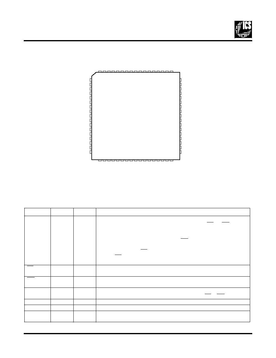
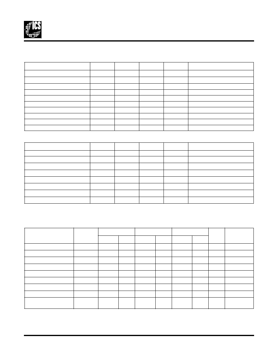
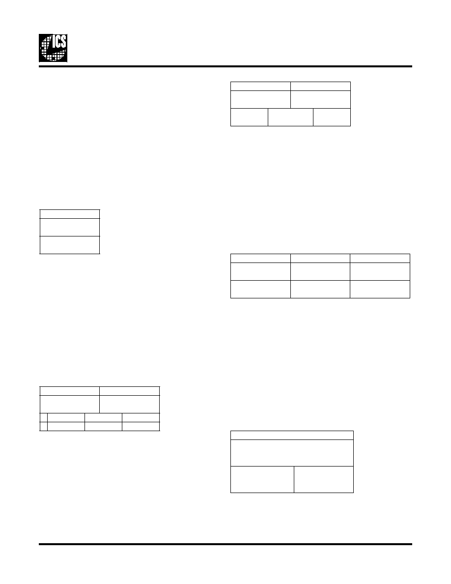
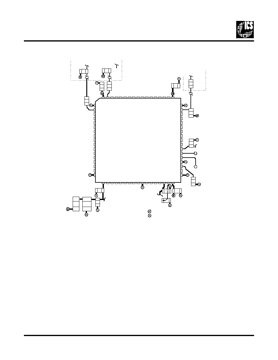
Pin Configuration
Pin Configuration
Pin Description (68-pin PLCC)
Symbol
Pin #
Type
Description
D7 - D0
21-14
I/O
Systems data bus bidirectional data I/O lines � used by host microprocessor for
internal register read and write operations (using active low RD and WR respec-
tively) for six internal registers: Pixel Address, Color Value, Pixel Mask, PLL
Address, PLL Parameter, and Command
During the write cycle, the rising edge of WR latches the data into the selected
register (set by the status of the three RS pins).
The rising edge of RD determines the end of the read cycle.
The RD set logical high indicates that data I/O lines no longer contain infor-
mation from the selected register and will be tri-stated.
RD
5
Input
RAM/PLL read enable bus control signal � in active low state, any information
present on the internal data bus is available on the Data I/O lines, D0-D7
WR
22
Input
Active low RAM/PLL write enable bus control signal � controls write timing on
microprocessor interface inputs, D0-D7
RS2-RS0
63,24,23
Input
Register address select 0 inputs � control selection of one of six internal registers �
inputs are sampled on falling edge of active enable signal (RD or WR)
XIN
48
Input
Crystal input � connect to 14.318 MHz crystal
XOUT
49
Output
Crystal output � connect to 14.318 MHz crystal
MSW
25
Input
Mode switch � digital control for selecting primary and secondary pixel color
modes � low selects primary mode � connect to ground if not used
AGND
N/C
N/C
N/C
N/C
N/C
N/C
N/C
N/C
N/C
RED
AVDD
CVDD
GRN
BLUE
RSET
DVDD
CGND
PCLK
P7
P6
P5
P4
P3
P2
P1
P0
XVDD
XGND
XOUT
XIN
VREF
N/C
DGND
5342_02
CLK0
P13
RD*
STROBE*
BLANK*
P9
CS1
CS0
P12
P11
CVDD
P10
P8
N/C
CVDD
SENSE*
36
35
34
33
32
31
30
29
28
27
40
39
38
37
43
42
41
60
59
58
57
56
55
54
53
52
51
50
49
48
47
46
45
44
1
2
3
4
5
6
7
8
9
68
64
65
66
67
61
62
63
GENDAC II
ICS5342
D0
D1
D2
D3
D4
D5
CGND
CLK1
P14
P15
WR*
RS0
RS1
MSW
CGND
10
11
12
13
14
15
16
17
18
19
20
21
22
23
24
25
26
D7
D6
RS2
ICS5342 (68-pin PLCC)
ICS5342
GENDAC
3
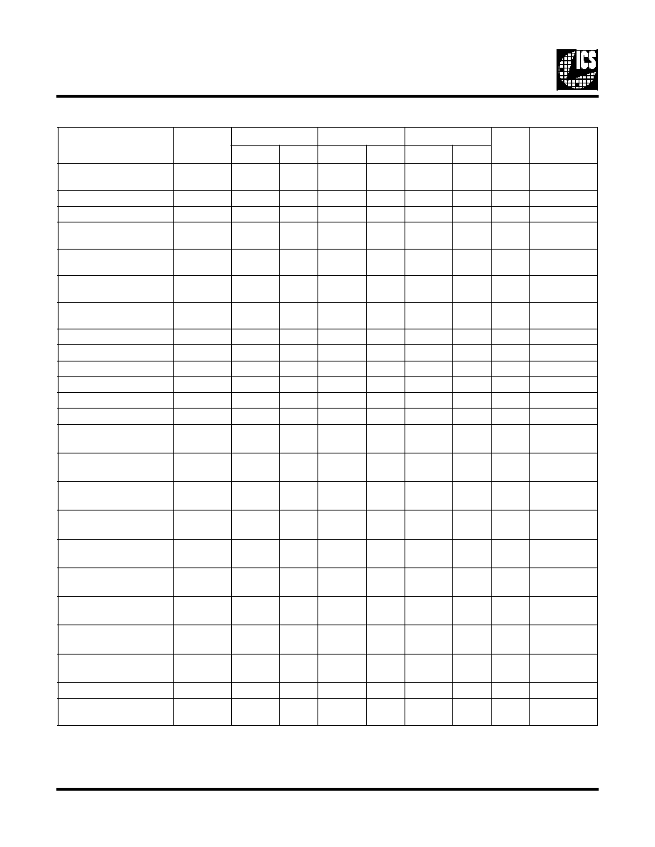
CLK1
11
Output
Memory clock output � used to time video memory
CLK0
8
Output
Video clock output � provides a CMOS level pixel or dot clock frequency to
graphics controller � output frequency is determined by values of PLL registers
CS0
2
Input
Clock select 0 � The status of CS0-1 determines which frequency is selected on
the CLK0 (video) output.
CS1
3
Input
Clock select 1� status of CS0-1 determines which frequency is selected on CLK0
(video) output
VREF
46
I/O
Internal reference voltage � normally connects to a 0.1
�
f capacitor to ground � to
use external Vref, connect 1.235V reference to this pin
RSET
42
Input
Resistor set � pin used to set current level in analog outputs � usually connected
through 1/4W, 1% resistor to ground
SENSE*
68
Output
Monitor sense � Pin is active low when any of red, green, or blue outputs >385mV.
Sense output is high when all analog outputs are < 275 mV. Chip has on-board
comparators and internal 1.235 V voltage reference. This signal is used to detect
monitor type.
BLUE
GREEN
RED
40
38
37
Output
Output
Output
Color signals from DAC analog outputs � Each DAC comprises several current
sources of which outputs are added together according to the applied binary value.
The outputs are typically used to drive a CRT monitor.
P15- P0
13,12,4,1
,
67-64,
58-51
Input
Pixel address lines � Byte-wide information is latched by the rising edge of PCLK
when using the color palette, and is masked by the Pixel Mask register. Values are
used to specify the RAM word address in default mode (accessing RAM). In Hi-
Color XGA, and True Color modes, they represent color data for the DACs.
Ground inputs if they are not used.
PCLK
59
Input
Pixel Clock � rising edge of PCLK controls latching of the Pixel Address and
BLANK* inputs � clock also controls progress of these values through the three-
stage pipeline of the Color Palette RAM, DAC, and outputs
STROBE*
6
Input
latches input clock select signals CS0-CS1
BLANK*
7
Input
Composite BLANK* Signal, active low. When BLANK* is asserted, outputs of
DACs are zero which blacks screen. DACs are automatically powered down to
save current during blanking. Color palette may still be updated through D0-D7
during blanking.
CVDD
9
-
CLK1 Power Supply � connect to DVDD
CVDD
27
-
CLK0 power supply � connect to AVDD
AVDD
41
-
DAC power supply � Connect to AVDD
DVDD
43
-
Digital power supply
XVDD
50
-
Crystal oscillator power supply� connect to AVDD
CVDD
61
-
CLK power supply � connect to DVDD
CGND
10
-
VSS for CLK1 � connect to ground.
CGND
26
-
VSS for CLK0 � connect to ground
XGND
47
-
VSS for crystal oscillator
AGND
36
-
DAC ground � connect to ground
DGND
44
-
Digital ground � connect to ground
CGND
60
-
VSS for CLK � connect to ground
N/C
28-35,
39,45,
62
-
Not connected � leave floating or tie to ground
Pin Description (68-pin PLCC)
Symbol
Pin #
Type
Description
ICS5342
GENDAC
4
Internal Registers
RS2
RS1
RS0
Register Name
Description (all registers can be written to and read from)
The GENDAC has a single pixel address register which can be
accessed through either register address 0,0,0 or 0,1,1 � reading
from either register gives the same result.
Writing a value to address 0,0,0:
� specifies an address within the color palette RAM
� initializes the Color Value register
Writing a value to address 0,1,1:
� specifies an address within the color palette RAM
� loads Color Value register with contents of location in
addressed RAM palette and then:
� increments Pixel Address register
0
1
1
Pixel Address
WRITE
Writing to this 8-bit register is done before writing one or more
color values to color palette RAM.
0
1
1
Pixel Address
READ
Writing to this 8-bit register is done before reading one or more
color values from color palette RAM.
0
0
1
Color Value
The 18-bit Color Value register acts as a buffer between the
microprocessor interface and the color palette. A value may be
read from or written to this register using a three-byte transfer
sequence. The color value is contained in the least significant 6
bits, D0-D5, of the byte read � the most significant 2 bits are set
to zero. The same 6 bits are used when writing a byte. When
reading or writing, data is transferred in the same order � red
byte first, then green, then blue. Each transfer between the Color
Value register and the color palette replaces the normal pixel
mapping operations of the GENDAC for a single pixel.
After writing three definitions to this register, its contents are
written to the location in the color palette RAM specified by the
Pixel Address register, before that register increments.
After reading three definitions from this register, the contents of
the location in the color palette RAM specified by the Pixel
Address registers are copied into the Color Value register, and
the Pixel Address register increments.
0
1
0
Pixel Mask
The 8-bit Pixel Mask register can be used to mask selected bits
of the Pixel Address value applied to the Pixel Address inputs
(P7-P0). A one in a position in the mask register leaves the corre-
sponding bit in the Pixel Address unaltered, while a zero sets
that bit to zero. The Pixel Mask register does not affect the Pixel
Address generated by the microprocessor interface when the pal-
ette RAM is being accessed.
1
0
0
PLL Address
WRITE
Writing to this 8-bit register is performed prior to writing one or
more PLL programming values to the PLL Parameter register.
1
1
1
PLL Address
READ
Writing to this 8-bit register is performed prior to reading one or
more PLL programming values from the PLL Parameter register.
ICS5342
GENDAC
5
1
1
0
Command
This 8-bit register selects color mode, for instance 8-bit Pseudo
Color, Hi-Color, True Color, or XGA, and DAC power down.
The registers are reset to pseudo color mode on power up.
1
0
1
PLL Parameter
There are 16 PLL parameter registers accessible as indexed by
Read/Write registers. Parameter registers 0F and 0D-00 are two
bytes long and 0E is one byte long. Register 0E is a control reg-
ister. The bits of this register include clock select and enable
functions, the rest contain PLL frequency parameters. After writ-
ing the start index address in the PLL address register, these reg-
isters can be accessed in successive two (or one) bytes. The
address register auto increments after one (0E) or two bytes to
access the entire register
Internal Registers
RS2
RS1
RS0
Register Name
Description (all registers can be written to and read from)
ICS5342
GENDAC
6
Note:
Stresses above those listed under Absolute Maximum Ratings may cause permanent damage to the device. This is a stress
rating only and functional operation of the device at these or any other conditions above those indicated in the operational sec-
tions of this specification is not implied. Exposure to absolute maximum rating conditions for extended periods may affect de-
vice reliability.
Electrical Characteristics
DC CHARACTERISTICS (note: J)
Parameter
Symbol
Min.
Max.
Units
Test Conditions
Positive supply voltage
V
DD
4.75
5.25
V
Input logic "1" voltage
V
IH
2.0
V
DD
+0.5
V
Input logic "0" voltage
V
IL
� 0.5
0.8
V
Reference current
I
REF
�7.0
�10
mA
Reference voltage
V
REF
1.10
1.35
V
Digital input current
I
IN
�
10
�
A
V
DD
=max, V
DD
V
IN
GND
Off-state digital output current
I
OZ
�
50
�
A
V
DD
= max, V
DD
V
IN
GND
Average power supply current
I
DD
250
mA
I
O
= max, Digital outputs
unloaded
DACs in power down mode
I
DACOFF
50
mA
no palette access
Sense logic "1"
V
OHS
2.4
V
I
O
= -0.4mA
Sense logic "0"
V
OLS
0.4
V
I
O
= 0.4mA
Clock logic "1"
V
OHC
2.4
V
I
O
= -12.0mA
Clock logic "0"
V
OLC
0.4
V
I
O
= 12.0mA
Logic "1"
V
OH
2.4
V
I
O
= -3.2mA, note K
Logic "0"
V
OL
0.4
V
I
O
= 3.2mA, note K
XIN input clock rise time
XCLK
r*
15
ns
TTL levels
XIN input clock fall time
XCLK
f*
15
ns
TTL levels
Frequency change of CLK0 and
CLK1 over supply and tempera-
ture
FD
0.05
%
with respect to typical frequency
Power Supply Voltage........................................................7 V
Voltage on any other pin.............. GND
�
0.5V to V
DD
+ 0.5V
Temperature under bias ................................ � 40� C to 85� C
Storage Temperature................................... � 65� C to 150� C
DC Digital Output Current ......................................... 25 mA
Analog Output Current ................................................ 45 mA
Reference Current ...................................................... �15 mA
Power Dissipation ......................................................... 1.0 W
Absolute Maximum Ratings
ICS5342
GENDAC
7
* Characterized values only
DAC Characteristics
Parameter
Symbol
Min
Max
Units
Test Conditions
Maximum output voltage
V
o
(max)
1.5
V
I
o
10 mA
Maximum output current
I
o
(max)
21
mA
V
o
1V
Full scale error
�
5
%
note A, B
DAC to DAC correlation
�
2
%
note B
Integral Linearity, 6-bit
�
0.5
LSB
note B
Integral Linearity, 8-bit
�
1
LSB
note B
Full scale settling time*, 6-bit
28
ns
note C
Full scale settling time*, 8-bit
20
ns
note C
Rise time (10% to 90%)*
6
ns
note C
Glitch energy*
200
pV.s
note C
PLL AC Characteristics
Parameter
Symbol
Min
Max
Units
Test Conditions
Clock 0 operating range
f0
25
135
MHz
Clock 1 operating range
f
1
25
135
MHz
Output clocks rise time*
t
r
3
ns
25 pF load, TTL levels
Output clocks fall time*
t
r
3
ns
25 pF load, TTL levels
Duty Cycle*
d
t
40/60
60/40
%
Jitter, one sigma*
j
1s
130 ps
ps
Jitter, absolute*
j
abs
-300 ps
300 ps
ps
Input reference frequency*
f
ref
5
25
MHz
Typically 14.318 MHz
AC Electrical Characteristics (note: J)
Parameter
Symbol
80 MHZ
110MHz
135Mhz
Units
Test
Conditions
Min
Max
Min
Max
Min
Max
PCLK period
t
CHCH
12.5
9.09
7.4
ns
PCLK jitter
t
CHCH
*
�
2.5
+2.5
%
note D
PCLK width low
t
CLCH
5
3.6
3
ns
PCLK width high
t
CHCL
5
3.6
3
ns
Pixel word setup time
t
PVCH
3
3
2
ns
note E
Pixel word hold time
t
CHPX
3
2
1
ns
note E
BLANK* setup time
t
BVCH
3
3
2
ns
note E
BLANK* hold time
t
CHBX
3
2
1
ns
note E
PCLK to valid DAC
output
t
CHAV
*
20
20
20
ns
note
F
ICS5342
GENDAC
8
Differential output
delay
t
CHAV
2
2
2
ns
note G
WR* pulse width low
t
WLWH
50
50
50
ns
RD* pulse width low
t
RLRH
50
50
50
ns
Register select setup
time
t
SVWL
10
10
10
ns
write cycle
Register select setup
time
t
SVRL
10
10
10
ns
read cycle
Register select hold
time
t
WLSX
10
10
10
ns
write cycle
Register select hold
time
t
RLSX
10
10
10
ns
read cycle
WR* data setup time
t
DVWH
10
10
10
ns
WR* data hold time
t
WHDX
10
10
10
ns
Output turn-on delay
t
RLQX
5
5
5
ns
RD* enable access time
t
RLQV
40
40
40
ns
Output hold time
t
RHQX
3
3
3
ns
Output turn-off delay
t
RHQZ
20
20
20
ns
note H
Successive write inter-
val
t
WHWL1
4
(t
CHCH
)
4
(t
CHCH
)
4
(t
CHCH
)
cycle
note I
WR* followed by read
interval
t
WHRL1
4
(t
CHCH
)
4
(t
CHCH
)
4
(t
CHCH
)
cycle
note I
Successive read interval
t
RHRL1
4
(t
CHCH)
4
(t
CHCH
)
4
(t
CHCH
)
cycle
note I
RD* followed by write
interval
t
RHWL1
4
(t
CHCH)
4
(t
CHCH
)
4
(t
CHCH
)
cycle
note I
WR* after color write
t
WHWL2
4
(t
CHCH)
4
(t
CHCH
)
4
(t
CHCH
)
cycle
note I
RD* after color write
t
WHRL2
4
(t
CHCH
)
4
(t
CHCH
)
4
(t
CHCH)
cycle
note I
RD* after color read
t
RHRL2
8
(t
CHCH
)
8
(t
CHCH
)
8
(t
CHCH)
cycle
note I
WR* after color read
t
RHWL2
8
(t
CHCH
)
8
(t
CHCH
)
8
(t
CHCH
)
cycle
note I
RD* after read address
write
t
WHRL3
8
(t
CHCH)
8
(t
CHCH
)
8
(t
CHCH
)
cycle
note I
SENSE* output delay
t
SOD
1
1
1
�
s
XIN input clock rise
time
t
XCLKR
*
15
15
15
ns
TTL levels
AC Electrical Characteristics (note: J)
Parameter
Symbol
80 MHZ
110MHz
135Mhz
Units
Test
Conditions
Min
Max
Min
Max
Min
Max
ICS5342
GENDAC
9
* Characterized values only
XIN input clock fall
time
t
XCLKF
*
15
15
15
ns
TTL levels
AC Electrical Characteristics (note: J)
Parameter
Symbol
80 MHZ
110MHz
135Mhz
Units
Test
Conditions
Min
Max
Min
Max
Min
Max
Notes:
A. Full scale error is derived from design equation:
{[(F.S.I
OUT
)R
L
� 2.1(I
REF
)R
L
] / [2.1(I
REF
)R
L
]} 100%
V
BLACK LEVEL
= 0 V
F.S.I
OUT
= Actual full scale measured output
B. R= 37.5
, I
REF
= � 8.88 mA
C. Z
I
= 37.5
+ 30 pF, I
REF
= � 8.88 mA
D. This parameter is the allowed Pixel Clock frequency
variation. It does not permit the Pixel Clock period to
vary outside the minimum values for Pixel Clock
(t
CHCH
) period.
E.
The color palette's pixel address is required to be a valid
logic level with the appropriate setup and hold times at
each rising edge of PCLK (this requirement includes the
blanking period).
F.
The output delay is measured from the 50% point of the
rising edge of CLOCK to the valid analog output. A
valid analog output is defined when the analog signal is
halfway between its successive values.
G. This applies to different analog outputs on the same
device.
H. Measured at
�
200 mV from steady state output voltage.
I.
This parameter allows synchronization between opera-
tions on the microprocessor interface and the pixel
stream being processed by the color palette.
J.
The following specifications apply for V
DD
= +5V
�
0.5V, GND=0. Operating Temperature = 0�C to 70�C.
K. Except for SENSE pin.
AC Test Conditions
Input pulse levels...................................................V
DD
to 3V
Input rise and fall times (10% to 90%) ............................ 3 ns
Digital input timing reference level ............................... 1.5 V
Digital output timing reference level .............0.8 V and 2.4 V
Capacitance
C
1
Digital input ............................................................... 7 pF
C
0
Digital output ............................................................. 7 pF
C
0A
Analog output ........................................................ 10 pF
Clock Load
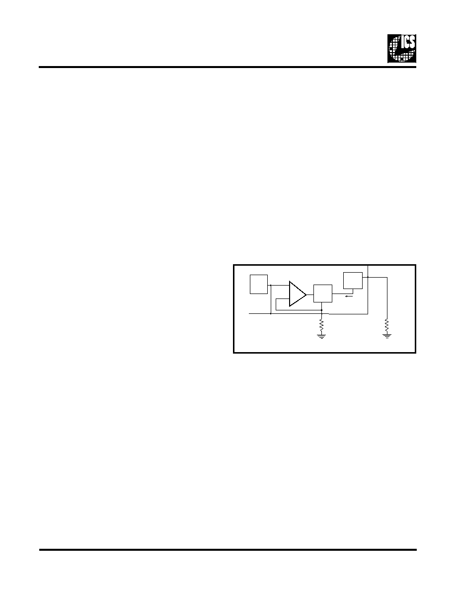
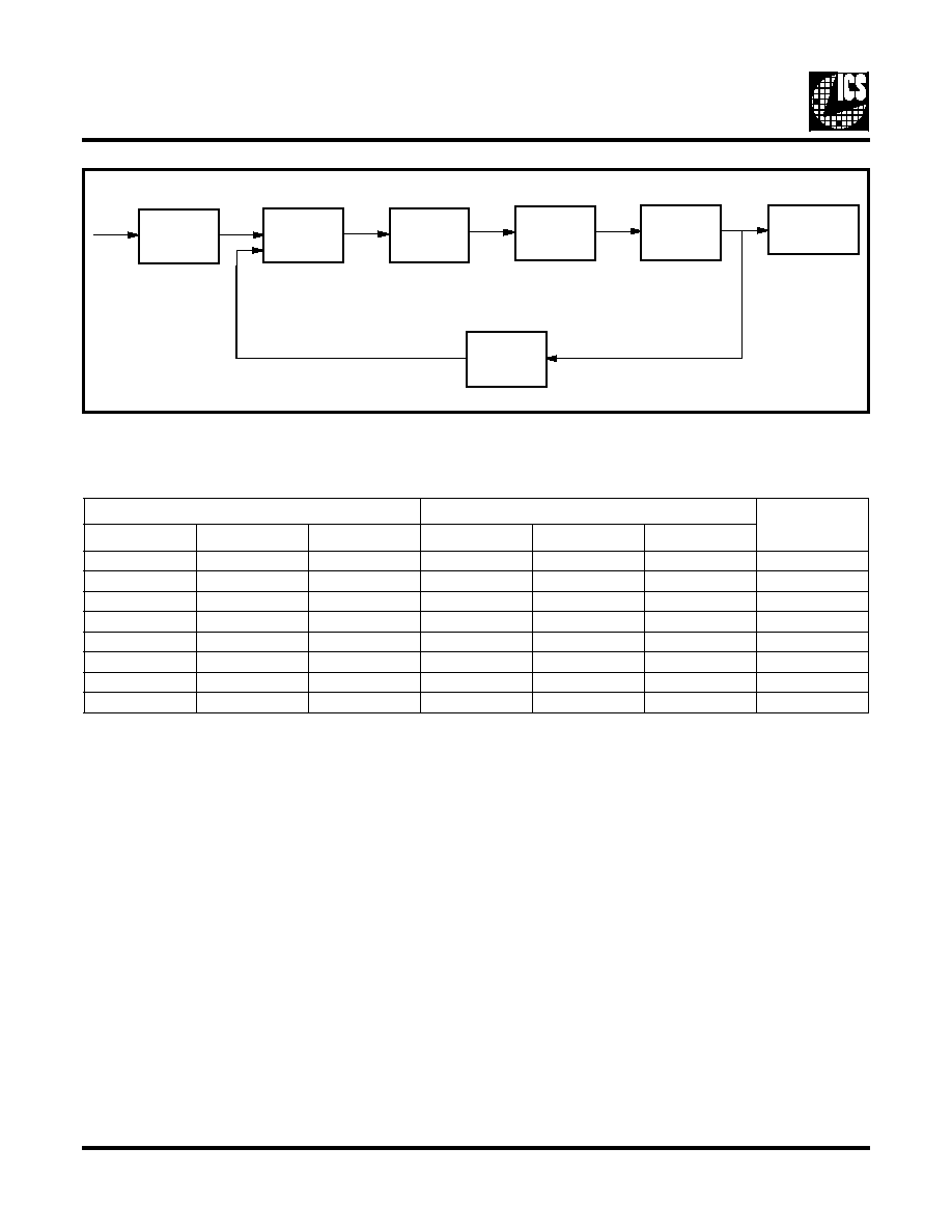
General Operation
The ICS5342 GENDAC is intended for use as the analog out-
put stage of raster scan video systems. It contains a high-
speed Random Access Memory of 256 x 18-bit words, three
6/8-bit high-speed DACs, a microprocessor/graphic control-
ler interface, a pixel word mask, on-chip comparators, and
two user programmable frequency generators.
An externally generated BLANK* signal can be applied to
pin 7 of the ICS5342. This signal acts on all three of the ana-
log outputs. The BLANK* signal is delayed internally so that
it appears with the correct relationship to the pixel bit stream
at the analog outputs.
A pixel word mask is included to allow the incoming pixel
address to be masked. This permits rapid changes to the effec-
CLK
25 pF
1.4V
200
5342_03
ICS5342
GENDAC
10
tive contents of the color palette RAM to facilitate such oper-
ations as animation and flashing objects. Operations on the
contents of the mask register can also be totally asynchronous
to the pixel stream.
The ICS5342 also includes dual PLL frequency generators
providing a video clock (CLK0) and a memory clock (CLK1),
both generated from a single 14.318 MHz crystal. There are
eight selectable CLK0 frequencies. All eight are programma-
ble. There are two selectable and programmable CLK1 fre-
quencies (fA, fB). Default values (Shown in tables: "Video
Clock Default Frequency Registers," and "Memory Clock
Default Frequency Registers") are loaded into the appropriate
registers on power up.
Video Path
The GENDAC supports nine different video modes and is de-
termined by bits 4-7 of the command register. The default
mode is the 8-bit Pseudo Color mode. The other modes are the
bypass 15-bit, 16-bit and 24 bit True Color modes in 8-bit and
16-bit interface, and the 16-bit Pseudo Color (2:1) mode with
2X Clock. The 24-bit True Color has sparse and packed
modes.
Pseudo Color
8-bit Interface
In this mode, Pixel Address, P7-P0 and BLANK* inputs are
sampled on the rising edge of the clock (PCLK) and any
change appears at the analog outputs after three succeeding
rising edges of the PCLK. The DAC output depends on the
data in the color palette RAM.
16-bit Interface
In this mode, Pixel Address, P15-P0 and BLANK* inputs are
sampled on the rising edge of the clock (PCLK) and any
change appears at the analog outputs after three succeeding
rising edges of the 2 x ICLK. ICLK frequency is twice the
PCLK input frequency. The DAC output depends on the data
in the color palette RAM.
Bypass Mode
The GENDAC supports seven different bypass modes: three
for byte transfers and four for word transfers. In these modes,
the address pins P0-P15 represent Color Data that is applied
directly to the DAC. The internal look-up table RAM is ig-
nored. During byte transfers, the P8-P15 inputs are"don't
care." Data is always latched on the rising edge of PCLK.
Byte or word framing is internally synchronized with the ris-
ing edge of BLANK*.
DAC Outputs
The outputs of the DACs are designed to be capable of pro-
ducing 0.7 V peak white amplitude with an I
REF
of 8.88 mA
when driving a doubly-terminated 75
load. This corre-
sponds to an effective DAC output load (R
EFFECTIVE
) of 37.5
. The formula for calculating I
REF
with various peak white
voltage/output loading combinations is given below:
Note that for all values of I
REF
and output loading:
The reference current I
REF
is determined by the reference
voltage V
REF
and the value of the resistor connected to R
SET
pin. V
REF
can be the internal band gap reference voltage or
can be overridden by an external voltage. In both cases:
DAC Setup
The BLANK* input to the GENDAC acts on all three of the
DAC outputs. When the BLANK* input is low, the DACs are
powered down.
The connection between the DAC outputs of the ICS5342 and
the RGB inputs of the monitor should be regarded as a trans-
mission line. Impedance changes along the transmission line
will result in the reflection of part of the video signal back
along the line. These reflections may result in a degradation
of the picture displayed by the monitor.
RF techniques should be observed to ensure good fidelity.
The PCB trace connecting the GENDAC to the off-board con-
nector should be sized to form a transmission line of the cor-
rect impedance. Correctly matched RF connectors should be
used for connection from the PCB to the monitor coaxial cable
and from that cable to the monitor.
There are two recommended methods of DAC termination:
double termination and buffered signal. Each is described be-
low with its relative merits.
I
REF
V
PEAKWHITE
2.1
R
EFFECTIVE
�
---------------------------------------------
=
V
BLACKLEVEL
0
=
I
REF
V
REF
R
SET
/
=
DAC
V
REF
(
INT
)
I
REF
V
REF
(EXT)
33
34
36
38
39
R
SET
R
EFF
I
REF
5342_04
ICS5342
GENDAC
11
Double Termination (Figure 1)
For this termination scheme, a load resistor is placed at both
the DAC output and the monitor input. The resistor values
should be equal to the characteristic impedance of the line.
Double termination of the DAC output allows both ends of the
transmission line between the DAC outputs and the monitor
inputs to be correctly matched.The result should be an ideal
reflection-free system.
This arrangement is relatively tolerant of variations in trans-
mission line impedance (e.g. a mismatched connector) since
no reflections occur from either end of the line. A doubly ter-
minated DAC output will rise faster than any singly terminat-
ed output because the rise time of the DAC outputs is
dependent on the RC time constant of the load.
Double Termination
If the GENDAC drives large capacitive loads (for instance
long cable runs), it may be necessary to buffer the DAC out-
puts. The buffer will have a relatively high input impedance.
The connection between the DAC outputs and the buffer in-
puts should also be considered as a transmission line. The
buffer output will have a relatively low impedance. It should
be matched to the transmission line between it and the monitor
with a series terminating resistor. The transmission line
should be terminated at the monitor.
Buffered Signal
SENSE Output
The GENDAC contains three comparators, one for each of the
DAC output R, G and B lines. The reference voltage to the
comparators is proportional to the V
REF
(internal or external)
and is typically 0.330 for V
REF
=1.235 Volts. The SENSE*
pin will be driven low when any analog video output is above
0.385 mV. SENSE* output will be high when all analog out-
puts are below 275 mV. This signal is used to detect the type
of (or lack of) monitor connected to the system.
PLL Clock
The ICS5342 has dual PLL frequency generators for generat-
ing the video clock (CLK0) and memory clock (CLK1) need-
ed for graphics subsystems. Both of these clocks are
generated from a single 14.318 MHz crystal or they can be
driven from an external clock source. The chip includes the
capacitors for the crystal and all of the components needed for
the PLL loop filters, minimizing board component count.
There are eight possible video clock, CLK0, frequencies (f0-
f7) which can be selected by the external pins CS1-CS0. All
clocks are software selectable by setting a bit in the PLL con-
trol register. Frequencies f0-f7 can be programmed for any
frequency by writing appropriate parameter values to the PLL
parameter registers. The default frequencies on power up are
commonly used video frequencies (see table "Video Clock
Default Frequency Registers"). At power up, the frequencies
can be selected by pins CS2-CS0. There are two programma-
ble memory clock frequencies (fA, fB). On power up this fre-
quency defaults to the frequency given in the table:
"MemoryClock Default Frequency Registers." The memory
clock transition between frequencies is smooth and glitch free
if the N2 PLL parameter is not changed from its previous set-
ting.
* With 14.318 MHz input.
R
LOAD
R
LOAD
MONITOR
ICS5342
Ground
Ground
5342_05
R
T
R
LOAD
MONITOR
ICS5342
Ground
Ground
R
S
5342_06
Video Clock (CLK0) Default Frequency Register *
fn
VCLK
(MHz)
M & N
Code
Comments
f0
25.175
7D 50
VGA0 (VGA Graphics)
f1
28.322
55 49
VGA1 (VGA Text)
f2
31.500
2A 43
VESA 640 x 480 @72 Hz
f3
36.00
77 4A
VESA 800 x 600 @56 Hz
f4
40.00
79 49
VESA 800 x 600 @60 Hz
f5
44.889
6F 47
1024 x 768 @43 Hz Inter-
laced
f6
65.00
74 2B
1024 x 768 @ 60 Hz,
640 x 480 Hi-Color @ 72
Hz
f7
75.00
71 29
VESA 1024 x 768 @ 70
Hz,
True Color 640 x 480
ICS5342
GENDAC
12
Microprocessor Interface
Below are listed the six microprocessor interface registers
within the ICS5342, and the register addresses through which
they can be accessed.
Asynchronous Access to Microprocessor Interface
Accesses to all registers may occur without reference to the
high speed timing of the pixel bit stream being processed by
the GENDAC. Data transfers between the color palette RAM
and the Color Value register, as well as modifications to the
Pixel Mask register, are synchronized to the Pixel Clock by
internal logic. This is done in the period between micropro-
cessor interface accesses. Thus, various minimum periods are
specified between microprocessor interface accesses to allow
the appropriate transfers or modifications to take place. Ac-
cess to PLL address, PLL parameter and to the command reg-
ister are asynchronous to the pixel clock.
The contents of the palette RAM can be accessed via the Col-
or Value register and the Pixel Address registers.
Writing to the color palette RAM
To set a new color definition, a value specifying a location in
the color palette RAM is first written to the Write mode Pixel
Address register. The values for the red, green and blue inten-
sities are then written in succession to the Color Value regis-
ter. After the blue data is written to the Color Value register,
the new color definition is transferred to the RAM, and the
Pixel Address register is automatically incremented.
Writing new color definitions to a set of consecutive locations
in the RAM is made easy by this auto-incrementing feature.
First, the start address of the set of locations is written to the
write mode Pixel Address register, followed by the color def-
inition of that location. Since the address is incremented after
each color definition is written, the color definition for the
next location can be written immediately. Thus, the color def-
initions for consecutive locations can be written sequentially
to the Color Value register without re-writing to the Pixel Ad-
dress register each time.
Reading from the RAM
To read a color definition, a value specifying the location in
the palette RAM to be read is written to the read mode Pixel
Address register. After this value has been written, the con-
tents of the location specified are copied to the Color Value
register, and the Pixel Address register automatically incre-
ments.
The red, green and blue intensity values can be read by a se-
quence of three reads from the Color Value register. After the
blue value has been read, the location in the RAM currently
specified by the Pixel Address register is copied to the Color
Value register and the Pixel Address again automatically in-
crements. A set of color values in consecutive locations can be
read simply by writing the start address of the set to the read
mode Pixel Address register and then sequentially reading the
color values for each location in the set. Whenever the Pixel
Address register is updated, any unfinished color definition
read or write is aborted and a new one may begin.
The Pixel Mask Register
The pixel address used to access the RAM through the pixel
interface is the result of the bitwise AND-ing of the incoming
pixel address and of the contents of the Pixel Mask register.
This pixel masking process can be used to alter the displayed
colors without altering the video memory or the RAM con-
tents. By partitioning the color definitions by one or more bits
in the pixel address, such effects as rapid animation, overlays,
and flashing objects can be produced.
The Pixel Mask register is independent of the Pixel Address
and Color Value registers.
The Command Register
The Command register is used to select the various GENDAC
color modes and to set the power down mode. On power up
this register defaults to an 8-bit Pseudo Color mode. This reg-
ister can be accessed by control pins RS2-RS0, or by a special
sequence of events for graphics subsystems that do not have
the control signal RS2. For graphic systems that do not have
RS2, this pin is tied low and an internal flag (HF: Hidden
Flag) is set when the pixel mask register is read four times
Memory Clock (CLK1) Default Frequency Register
fn
MCLK
(MHz)
M & N
Code
Comments
fA
45.00
4F 2B
Memory and GUI sub-
system clock
fB
55.00
79 2E
Memory and GUI sub-
system clock
Microprocessor Interface Registers
RS2
RS1
RS0
Register Name
0
0
0
Pixel Address (write mode)
0
1
1
Pixel Address (read mode)
0
0
1
Color Value
0
1
0
Pixel Mask
1
0
0
PLL Address (write mode)
1
0
1
PLL Parameter
1
1
0
Command
1
1
1
PLL Address (read mode)
0/HF
1
0
Command Register accessed by
(hidden) flag after special
sequence of events.

ICS5342
GENDAC
13
consecutively. Once the flag is set, the following Read or
Write to the pixel mask register is directed to the command
register. The flag is reset for read or write to any register other
than the Pixel Mask register. The sequence has to be repeated
for any subsequent access to the command register.
The PLL Parameter Register
The CLK0 and CLK1 of the ICS5342 can be programmed for
different frequencies by writing different values to the PLL
parameter register bank. There are eight registers in the pa-
rameter register; seven are two bytes long and one (0E) is one
byte long.
Writing to the PLL parameter register
To write the PLL parameter data, the corresponding address
location is first written to the PLL address register. For soft-
ware compatibility with other chips, two address registers are
defined: the write mode PLL address register and the read
mode PLL address register. These are actually a single Read/
Write register in the ICS5342. The next PLL parameter write
will be directed to the first byte of the address location speci-
fied by the PLL address register. The next write to the param-
eter register will automatically be to the second byte of this
register. At the end of the second write the address is automat-
ically incremented. For the one byte "0E" register the address
location is incremented after the first byte write. If this fre-
quency is selected while programming, the output frequency
will change at the end of the second write.
Reading the PLL parameter register
To read one of the registers of the PLL parameter register the
address value corresponding to the location is first written to
the PLL address register. The next PLL parameter read will be
directed to the first byte of the address location pointed by this
index register. A next read of the parameter register will auto-
matically be the second byte of this register. At the end of the
second read, the address location is automatically increment-
ed. The address register (0E) is incremented after the first byte
read.
ICS5342
GENDAC
14
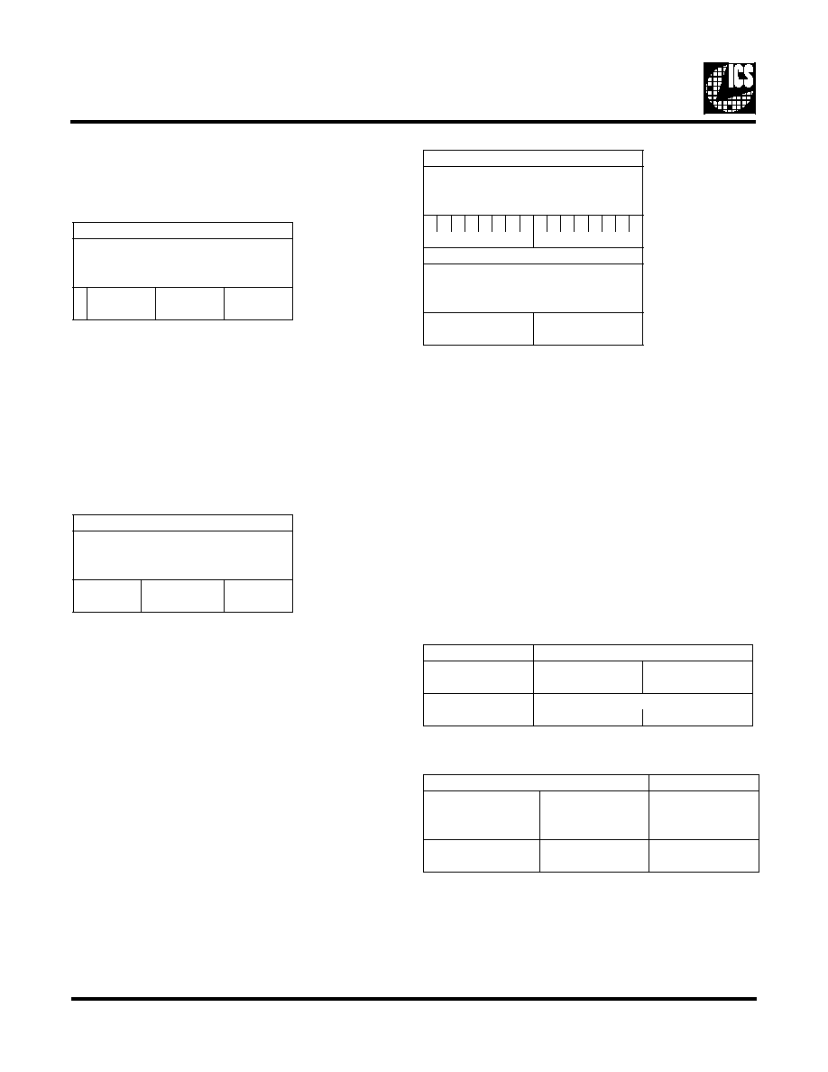
Functional Description
This section describes the register address and bit definition
for the RAMDAC and the Frequency Synthesizer sections.
Color Palette
Command Register
(RS0-RS2 = 011)
(RS0-RS1 = 01 with hidden flag)
By setting bits 4 and 7-5 in the command register the
ICS5342 can be programmed for different color modes and
the DACs can be turned off for low power operation.
Bit 7-4
Color Mode Select - These three bits select the
Color Mode of RAMDAC operation as shown in
the following table "Color Mode Select" (default
is 0 at power up).
Bit 3-2
(Reserved) Set to `0' for future compatibility.
Bit 1
Test Mode - When bit 1 is set checksum accumu-
lation is enabled. If bit 0 is also set the oscillator
and synthesizers are turned off for minimum
noise.
Bit 0
Power Down Mode of RAMDAC - When this bit
is set to 0 (default is 0), the device operates nor-
mally. If this bit is set to 1, the power and clock
to the Color Palette RAM and DACs are turned
off. The data in the Color Palette RAM are still
preserved. The CPU can access without loss of
data by internal automatic clock start/stop con-
trol. The DAC outputs become the same as
BLANK* (sync) level output during power down
mode. This bit does not affect the PLL clock syn-
thesizer function unless test mode is enabled.
Command Registers
7
6
5
4
3
2
1
0
2
1
0
3
Reserved = 0
Test mode
Snooze
Color Mode Select
8-BIT INTERFACE
Mode
Number
CM3
(CR4)
CM2
(CR7)
CM1
(CR6)
CM0
(CR5)
Color Mode
Clock Cycles/
Pixel Bits
0
0
0
0
0
8-bit Pseudo Color With Palette (default)
1
1
0
0
0
1
15-bit Direct Color With Bypass (Hi-Color)
2
3
0
0
1
0
24-Bit True Color With Bypass (True Color)
3
2
0
0
1
1
16-bit Direct Color With Bypass (XGA)
2
1
0
1
0
0
15-bit Direct Color With Bypass (hi-color)
2
1
0
1
0
1
15-bit Direct Color With Bypass (Hi-Color)
2
2
0
1
1
0
15-bit Direct Color With Bypass (Hi-Color)
2
3
0
1
1
1
24-bit True Color With Bypass (True Color)
3
16-BIT INTERFACE
Mode
Number
CM3
(CR4)
CM2
(CR7)
CM1
(CR6)
CM0
(CR5)
Color Mode
Clock Cycles/
Pixel Bits
4
1
0
0
0
Multiplexed 16-bit Pseudo Color With Palette
1/2
5
1
0
0
1
15-bit Direct Color With Bypass (Hi-Color)
1
6
1
0
1
0
16-bit Direct Color With Bypass (XGA
1
7
1
0
1
1
24-bit True Color With Bypass (True Color)
2
8
1
1
0
0
24-bit Packed True Color With Bypass
(true-color)
3/2
1
1
0
1
Reserved
1
1
1
0
Reserved
1
1
1
1
Reserved
ICS5342
GENDAC
15
Color Modes
The nine selectable color modes are described here. Four are
eight-bit and five are 16-bit wide pixel input. Color Modes 0-3
are 8-bit interfaces with bits P0-P7; P8-P15 are "don't care"
bits.
Mode 0: 8-bit Pseudo Color (one clock per pixel). This mode
is the 8-bit per pixel Pseudo Color mode. In this mode, inputs
P0-P7 are the pixel address for the color palette RAM and are
latched on the rising edge of every PCLK. This is the default
mode on power up and it is selected by setting bits CR7-CR4
to 0000.
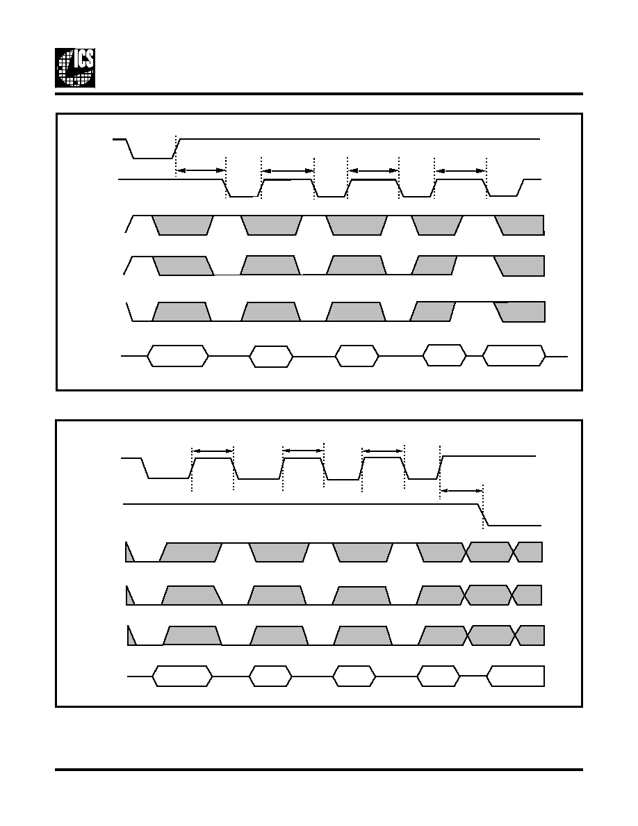
Mode 1: (15-bit per color bypass Hi-Color mode). This mode
is the 15-bit per pixel bypass mode. In this mode, inputs P0-P7
are the color DATA and are input directly to the DAC, by-
passing the color palette. The two bytes of data are latched in
two successive PCLK rising edges. ICS5342 supports only
the two clock mode and does not support the mode where the
data are latched on the rising and the falling edges. For com-
patibility, the 15/16 one clock modes are selected as two clock
modes in this chip. The low-byte, high byte synchronization
is internally done by the rising edge of BLANK*. Each color
is 5-bit wide and is packed into two bytes as shown below.
This mode can be selected by setting bits CR7-CR4 to 0010,
1000 or 1010.
3LSB = set to zero
Mode 2: (16-bit per pixel bypass XGA mode). This mode is
the 16-bit per pixel bypass mode and the P0-P7 inputs to go to
the DAC directly, bypassing the color palette. The 2 bytes
data is latched on two successive rising edges and the low-
byte, high-byte synchronization is internally done by the ris-
ing edge of BLANK*. In this mode, blue and red colors are 5
bits wide and green is 6 bits wide. The 2 bytes of data are
packed as shown below. This mode can be selected by setting
bits CR7-CR4 to 0110 or 1100.
2LSB = set to zero (green)
3LSB = set to zero (blue, red)
Mode 3: (24-bit per pixel True Color Mode). This mode is the
24-bit per pixel bypass mode. The three bytes of data are
latched on three successive PCLK edges and the first byte is
synchronized by the rising edge of BLANK*. In this mode,
each of the colors are 8-bit wide and the DAC is an 8-bit wide
DAC. The first byte is blue followed by green and red. This
mode can be selected by setting bits CR7-CR4 to 0100 or
1110. The DAC outputs changes every three cycles and the
pipeline delay from the first byte to output is five cycles.
16 bit Color Modes
Modes 4 - 8 use the 16-bit pixel interface.
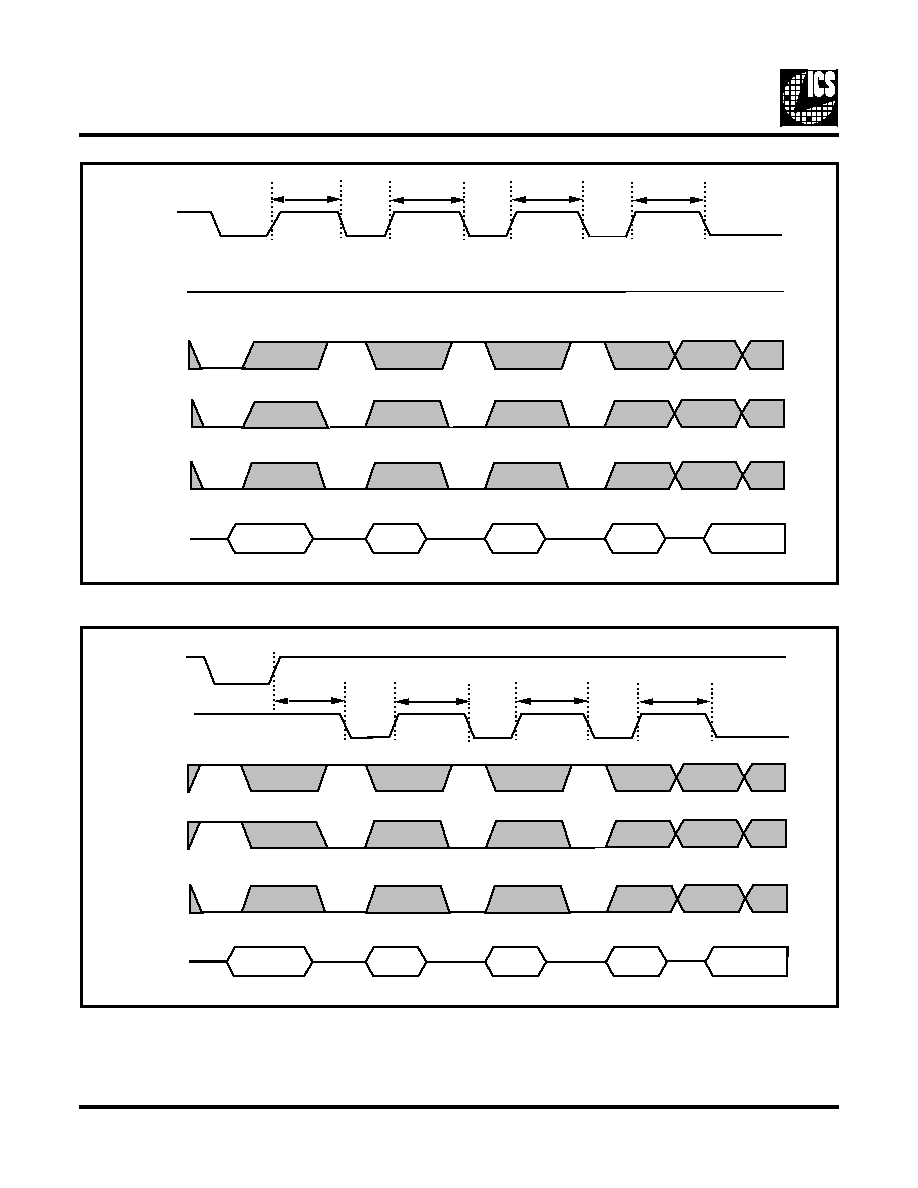
Mode 4: (8-bit Pseudo Color two pixels per clock) In this
mode, inputs P0-P15 are latched on the rising edge of every
PCLK. P0-7 and P8-P15 are used for successive addresses for
the palette RAM using an internal clock (ICLK) that runs at
twice the PCLK frequency. The DAC outputs change twice
for every PCLK and the pipeline delay from the first word to
output is one and one half cycles. This mode can be selected
by setting bits CR7-CR4 to 0001.
Mode 5: (16-bit pixel interface, 15-bit per color bypass Hi-
Color Mode) In this mode inputs P0-P15 are the color data
and are input directly to the DAC, bypassing the color palette.
The data is latched by the rising edge of PCLK and is pipe-
8-bit Pseudo Color
- Mode 0
PIXEL BYTE
P
7
P
6
P
5
P
4
P
3
P
2
P
1
P
0
7 6 5 4 3 2 1 0
LUT ADDRESS
15-Bit Color - Mode 1
SECOND BYTE
FIRST BYTE
P P P P P P P P P P P P P P P P
7 6 5 4 3 2 1 0 7 6 5 4 3 2 1 0
X 7 6 5 4 3 7 6 5 4 3 7 6 5 4 3
X RED
GREEN
BLUE
16-Bit Color - Mode 2
SECOND BYTE
FIRST BYTE
P P P P P P P P P P P P P P P P
7 6 5 4 3 2 1 0 7 6 5 4 3 2 1 0
7 6 5 4 3 7 6 5 4 3 2 7 6 5 4 3
RED
GREEN
BLUE
24-bit Color - Mode 3
THIRD BYTE
SECOND BYTE
FIRST BYTE
P P P P P P P P P P P P P P P P P P P P P P P P
7 6 5 4 3 2 1 0 7 6 5 4 3 2 1 0 7 6 5 4 3 2 1 0
7 6 5 4 3 2 1 0 7 6 5 4 3 2 1 0 7 6 5 4 3 2 1 0
RED
GREEN
BLUE
Multiplexed 8-bit Pseudo Color Word
- Mode 4
PIXEL WORD
P P P P P P P P P P P P P P P P
1 1 1 1 1 1 9 8 7 6 5 4 3 2 1 0
5 4 3 2 1 0
7 6 5 4 3 2 1 0 7 6 5 4 3 2 1 0
2nd PIXEL
ADDRESS
1st PIXEL
ADDRESS
ICS5342
GENDAC
16
lined to the DAC. The pipeline delay from input to DAC out-
put is three PCLK cycles. Each color is 5-bit wide as shown
below. This mode is selected by setting bits CR7-CR4 to
0011.
3LSB = set to zero
Mode 6: (16-bit pixel interface, 16-bit per color bypass XGA
mode) In this mode input P0-P15 are the color data and are in-
put directly to the DAC bypassing the color palette. The data
is latched by the rising edge of PCLK and is pipelined to the
DAC. The pipeline delay, from input to DAC output, is three
PCLK cycles. In this mode Blue and Red colors are 5 bits
wide, and Green is 6 bits wide. This mode is selected by set-
ting bits CR7-CR4 to 0101.
2LSB = set to zero (GREEN)
3LSB = set to zero (BLUE, RED)
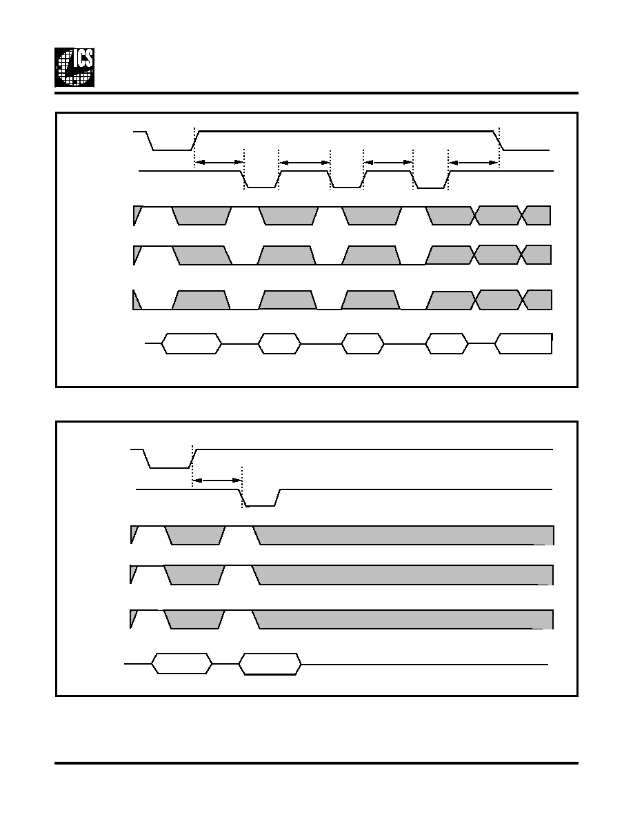
Mode 7: (16-bit pixel interface, 24-bit per color bypass
TRUE color mode) In this mode inputs P0-P15 are the color
data and are input directly to the DAC bypassing the color pal-
ette. Two words are latched on two successive rising edge of
PCLK to form the 24-bit DAC input. The first word and the
lower byte of the second word form the 24-bit pixel input to
the DAC. The higher byte of the second word is ignored. The
low and high word synchronization is internally done by the
rising edge of BLANK*. The pipeline delay from latching of
the first word to DAC output is 4 cycles and each pixel is two
pixel clocks wide. In this mode, each of the colors are 8-bits
wide and the DAC is 8-bit wide DAC. The first byte is Blue
followed by Green and Red. This mode is selected by setting
bits CR7-CR4 to 0111.
Mode 8: (16-bit pixel interface packed 24-bit per color bypass
TRUE color mode) In this mode inputs P0-P15 are the color
data and are input directly to the DAC bypassing the color pal-
ette. Three words are latched on three successive rising edges
of PCLK to form two successive 24-bit DAC inputs. The 16-
bit first word and the lower byte of the second word from the
first 24-bit pixel input and the second byte of the second word
with the 16 bits of the third word from the second 24-bit pixel
input. This cycle repeats every three cycles. The three-word
synchronization is internally done by the rising edge of
BLANK*. The pipeline delay from latching of first word to
DAC output is 3 1/2 cycles and each of the colors are 8-bits
wide and DAC is 8-bit wide DAC. The first byte is Blue fol-
lowed by Green and Red. This mode is selected by setting bits
CR7-CR4 to 1001.
15-Bit Color Word - Mode 5
PIXEL WORD
P P P P P P P P P P P P P P P P
1 1 1 1 1 1 9 8 7 6 5 4 3 2 1 0
5 4 3 2 1 0
X 7 6 5 5 4 7 6 5 4 3 7 6 5 4 3
X RED
GREEN
BLUE
16-Bit Color Word - Mode 6
PIXEL WORD
P P P P P P P P P P P P P P P P
1 1 1 1 1 1 9 8 7 6 5 4 3 2 1 0
5 4 3 2 1 0
7 6 5 4 3 7 6 5 4 3 2 7 6 5 4 3
RED
GREEN
BLUE
24-Bit Direct Color Word - Mode 7
FIRST WORD
P P P P P P P P P P P P P P P P
1 1 1 1 1 1 9 8 7 6 5 4 3 2 1 0
5 4 3 2 1 0
7 6 5 4 3 2 1 0 7 6 5 4 3 2 1 0
GREEN
BLUE
SECOND WORD
P P P P P P P P P P P P P P P P
1 1 1 1 1 1 9 8 7 6 5 4 3 2 1 0
5 4 3 2 1 0
X X X X X X X X 7 6 5 4 3 2 1 0
IGNORED
RED
Packed 24-bit Word - Mode 8
1st DAC Cycle
SECOND WORD FIRST WORD
P P P P P P P P P P P P P P P P P P P P P P P P
7 6 5 4 3 2 1 0 1 1 1 1 1 1 9 8 7 6 5 4 3 2 1 0
7 6 5 4 3 2 1 0 5 4 3 2 1 0 9 8 7 6 5 4 3 2 1 0
RED
GREEN
BLUE
2nd DAC Cycle
THIRD WORD
SECOND WORD
P P P P P P P P P P P P P P P P P P P P P P P P
1 1 1 1 1 1 9 8 7 6 5 4 3 2 1 0 1 1 1 1 1 1 9 8
5 4 3 2 1 0
5 4 3 2 1 0
7 6 5 4 3 2 1 0 7 6 5 4 3 2 1 0 7 6 5 4 3 2 1 0
RED
GREEN
BLUE
ICS5342
GENDAC
17
Frequency Generators
The ICS5342 clock synthesizer can be reprogrammed through
the microprocessor interface for any set of frequencies. This
is done by writing appropriate values to the PLL Parameter
Register Bank (See following table: "PLL Parameter Regis-
ters").
PLL Address Registers
The address of the parameter register is written to the PLL ad-
dress registers before accessing the parameter register. This
register is accessed by register select pins RS2-RS0 = 100 or
111.
PLL Parameters Registers
There are sixteen registers in the PLL parameter register (ta-
ble 5). Registers 00 to 07 are for the CLK0 selectable frequen-
cy list, Register 0A and 0B for CLK1 programmable
frequency and register 0E is the PLL control register.
PLL Control Register
Bits in this register determine internal or external CLK0 se-
lect.
Bit 7,6, 3 Reserved, set to `0' for future compatibility.
Bit 5
Enable Internal Clock Select (INCS) for CLK0.
When this bit is set to 1, the CLK0 output fre-
quency is selected by bits 2-0 in this register.
External pins CS0-CS2 are ignored.
Bit 4
Clk1 Select when this bit is set to 0, fA is
selected. When it is set to 1, fB is selected. The
default is 0 for fA selected at power up.
Bit 2 - 0
Internal Clock Select for CLK0 (INCS). These
three bits select the CLK0 output frequency if bit
5 of this register is on. They are interpreted as an
octal number, n, that selects fn. Default selects f0.
PLL Data Registers
The CLK0 and CLK1 output frequency is determined by the
parameter values in this register. These are two-byte registers;
the first byte is the M-byte and the second the N-byte.
M-Byte PLL Parameter Input
The M-byte has a 7-bit value (1-127) which is the feedback
divider of the PLL.
N-Byte PLL Parameter Input
The N-byte contains two parameter values. N1 sets a 5-bit val-
ue (1-31) for the input pre scalar and N2 is a 2-bit code for se-
lecting 1, 2, 4, or 8 post divide clock output.
PLL Address Register
7 6 5 4 3 2 1 0
PLL Register Adr.
7 6 5 4 3 2 1 0
PLL Parameter Registers
Index
R/W
Register
00
R/W
CLK0 f0 PLL Parameters
(2 bytes)
01
R/W
CLK0 f1 PLL Parameters
(2 bytes)
02
R/W
CLK0 f2 PLL Parameters
(2 bytes)
03
R/W
CLK0 f3 PLL Parameters
(2 bytes)
04
R/W
CLK0 f4 PLL Parameters
(2 bytes)
05
R/W
CLK0 f5 PLL Parameters
(2 bytes)
06
R/W
CLK0 f6 PLL Parameters
(2 bytes)
07
R/W
CLK0 f7 PLL Parameters
(2 bytes)
08
R/-
(Reserved) = 0
(2 bytes
09
R/W
CLK1 fA PLL
(2 bytes)
0A
R/W
CLK1 fB PLL
(2 bytes)
0B
R/W
(Reserved) = 0
(2 bytes
0C
R/-
(Reserved) = 0
(2 bytes)
0D
R/-
(Reserved) = 0
(2 bytes)
0E
R/W
PLL Control Register
(1-byte)
0F
R/-
(Reserved) = 0
(2 bytes)
PLL Control Register
7
6
5
4
3
2
1
0
(RV)=
0
(RV)=
0
ENBL
INCS
CLK1
SEL
(RV)=
0
Internal Select
X
X
X
M-Byte
7
6
5
4
3
2
1
0
Reserved
= 0
M-Divider Value
X
X
X
X
X
X
X
N-Byte PLL Parameter Input
7
6
5
4
3
2
1
0
Reserved
= 0
N2 - Code
N1-Divider Value
X
X
X
X
X
X
X
ICS5342
GENDAC
18
N2 Post Divide Code
If mode 4 is set in the command register, CR7-CR4 bits equal
0001, and the N2 code must be 10.
The block diagram of the PLL clock synthesizer is shown in
figure 3.
Based on the M and N values, the output frequency of the
clocks is given by the following equation:
M and N values should be programmed such that the frequen-
cy of the VC0 is within the optimum range for duty cycle, jit-
ter and glitch free transition. Optimum duty cycle is achieved
by programming N2 for values greater than unity. See the next
section for a programming example.
Programming Example
Suppose an output frequency of 25.175 MHz is desired. The
reference crystal is 14.318 MHz. The VCO should be targeted
to run in the 60 to 270 MHz range, so choosing a post divide
of 4 gives a VCO frequency of:
From the table in the previous section, we find N2 = 2 Substi-
tuting F
REF
= 14.318 and 2
N2
= 4 into the clock frequency
equation in the previous section:
By trial and error:
M + 2 = 127 M = 125
N1 + 2 = 18 N1 = 16
so the registers are:
M = 125d = 1 1 1 1 1 0 1 b
N = 0 & N2 code & N1 = 0 & 1 0 & 1 0 0 0 0
N = 0 1 0 1 0 0 0 0 b
Additional Information on Programming
the Frequency Generator section of the
GENDAC
When programming the GENDAC PLL parameter registers,
there are many possible combinations of parameters which
will give the correct output frequency. Some combinations are
better than others, however. Here is a method to determine
how the registers need to be set:
The key guidelines come from the operation of the phase
locked loop, which has the following restrictions:
1.
This refers to the input refer-
ence frequency. Most users simply connect a 14.318
MHz crystal to the crystal inputs, so this is not a prob-
lem.
2.
This is the frequency input to
the phase detector.
3.
This is the VCO
frequency. In general, the VCO should run as fast as pos-
sible, because it has lower jitter at higher frequencies.
Also, running the VCO at multiples of the desired fre-
quency allows the use of output divides, which tends to
improve the duty cycle.
4.
This is the output fre-
quency.
These rules lead to the following procedure for determining
the PLL parameters, assuming rules 1 and 4 are satisfied.
A. Determine the value of N2 (either 1, 2, 4 or 8) by select-
ing the highest value of N2, which satisfies the condition
N2* fCLK < 270 Mhz.
B. Calculate:
C. Now (M+2) and (N1+2) must be found by trial and error.
With a 14.318 MHz reference frequency, there will gen-
erally be a small output frequency error due to the reso-
lution limit of (M+2) and (N1+2). For a given frequency
tolerance, several different (M+2) and (N1+2) combina-
tions can usually be found. Usually, a few minutes trying
N2 Post Divide Code
N2 Code
Divider
00
1
01
2
10
4
11
8
F
OUT
M
2
+
(
)
F
REF
2
N 2
N1
2
+
(
)
---------------------------------
=
4
25.175
�
101.021 MHz
=
25.175
14.318
---------------- 4
M
2
+
N1
2
+
-----------------
=
2 MHz
f
REF
25 MHz
<
<
600KHz
f
REF
N1
2
+
-----------------
8MHz
60MHz
M
2
+
N1
2
+
----------------- f
REF
270 MHz
f
CLK 0
and f
CLK 1
35 MHz
M
2
+
N 1
2
+
-----------------
2
N 2
f
OUT
f
REF
-----------------------
=
ICS5342
GENDAC
19
out numbers with a calculator will produce a workable
combination. Multiplying possible values of (N1+2) by
the desired ratio will indicate approximately the value of
M. This method is shown in the example below. A pro-
gram could be written to try all possible combinations of
(M+2) and (N1+2) (3937 possible combinations). Dis-
card those outside the error band, and select from those
remaining by giving preference to ratios which use lower
values of (M+2). Lower values of (M+2) and (N1+2)
provide better noise rejection in the phase locked loop.
Example: Suppose you have a 14.318 MHz reference crystal
and want an output frequency of 66 MHz. You want to limit
the VCO frequency to 240 Mhz and have an error of no great-
er than 0.5%. What are the values of the PLL data registers?
A. 66*8 = 528 > 250 -- VCO speed too high
66*4 = 264 > 250 -- VCO speed too high
66*2 = 132 < 250 -- VCO speed OK, N2 = 2, N2 code =
01 from the Post Divide Code table in the PLL Data
Registers section.
B. 132/14.31818 = 9.219 This is the desired frequency mul-
tiplication ratio.
C. Setting (N1+2) = 3,4, ...12, 13 and performing some
simple calculations yields the following table: (Note that
N1 cannot be 0).
The ratio 83/9 is closest. Thus:
(N2+2) = 9
N2=7
(M+2) = 83
M = 81
The M-byte PLL parameter word is simply 81 in binary, plus
bit 7 (which must be set to 0), or 01010001. The N-byte PLL
parameter word is N2 code (01) concatenated with 5 bits of
N2 in binary (00111), or 00100111. Once again, bit 7 must be
zero.
The combination with the least frequency error was chosen,
but several other combinations are within the 0.5% tolerance.
Because the lowest value of (M+2) offers the best damping,
the 37/4 combination will have the best power supply rejec-
tion. This results in lower jitter due to external noise.
Example Calculation of PLL Data Register Values
(N1 + 2)
(N1 + 2) *9.219
rounded (=M + 2)
Actual Ratio
Percent Error
3
27.657
28
9.33
-1.23
4
36.876
37
9.25
-0.34
5
46.095
46
9.20
0.21
6
55.314
55
9.17
0.57
7
64.533
65
9.29
-0.72
8
73.752
74
9.25
-0.34
9
82.971
83
9.22
-0.03
10
92.19
92
9.20
0.21
11
101.409
101
9.18
0.40
12
110.628
111
9.25
-0.34
13
119.847
120
9.23
-0.13
ICS5342
GENDAC
20
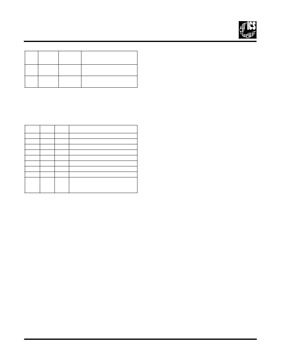
PLL Clock Synthesizer Block Diagram
Video Clock Selection Table
External Select
(Internal Select PLL Control Register)
CLK 0
Frequency
CS2
CS1
CS0
BIT 2
BIT 1
BIT 0
0
0
0
0
0
0
f0
0
0
1
0
0
1
f1
0
1
0
0
1
0
f2
0
1
1
0
1
1
f3
1
0
0
1
0
0
f4
1
0
1
1
0
1
f5
1
1
0
1
1
0
f6
1
1
1
1
1
1
f7
1/(N1+2)
F
ref
PHASE
DETECT
CHARGE
PUMP
LOOP
FILTER
VCO
N2
COUNTER
1/(M1+2)
5342_07
ICS5342
GENDAC
21
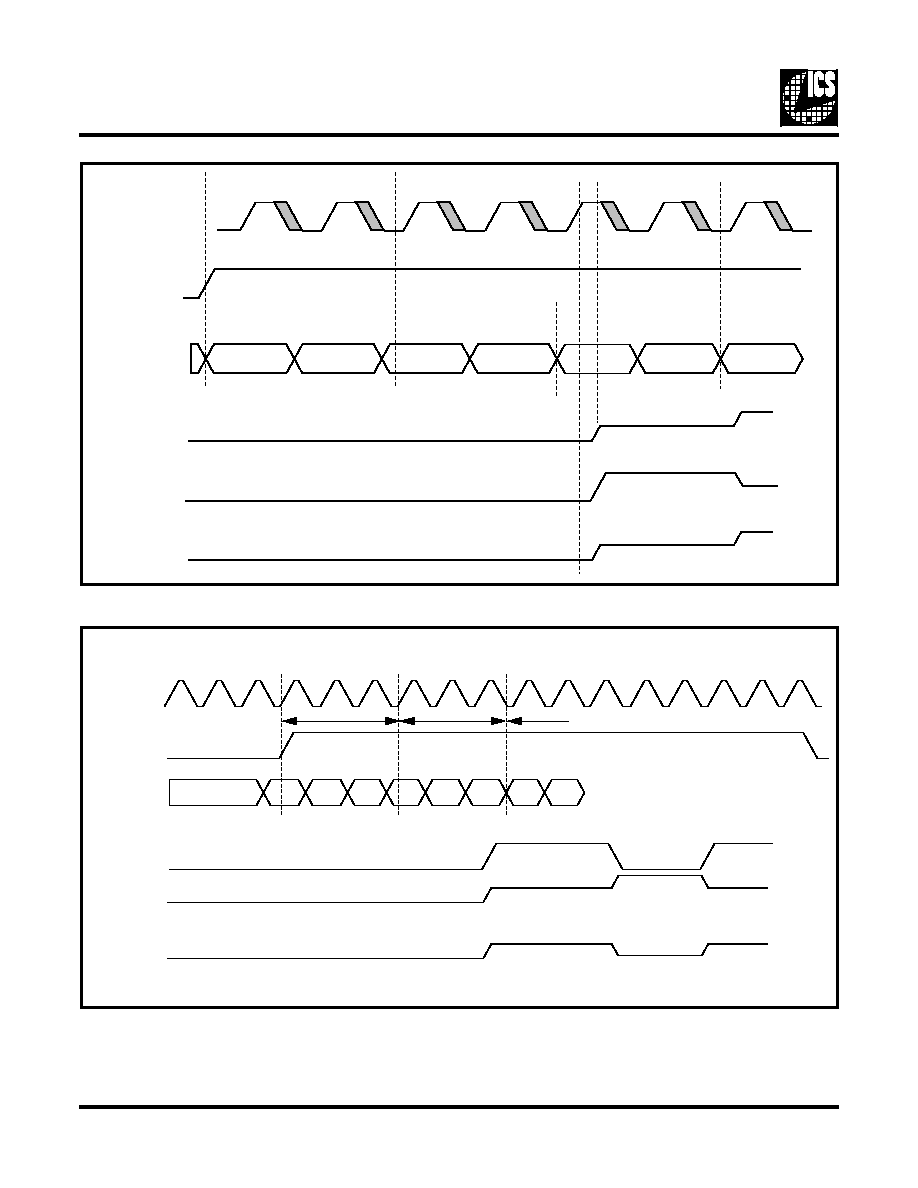
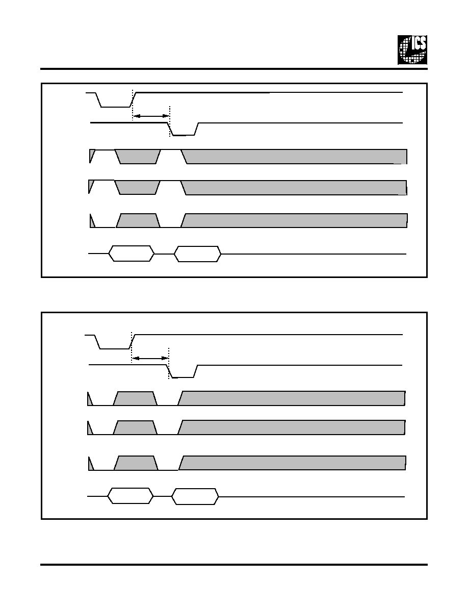
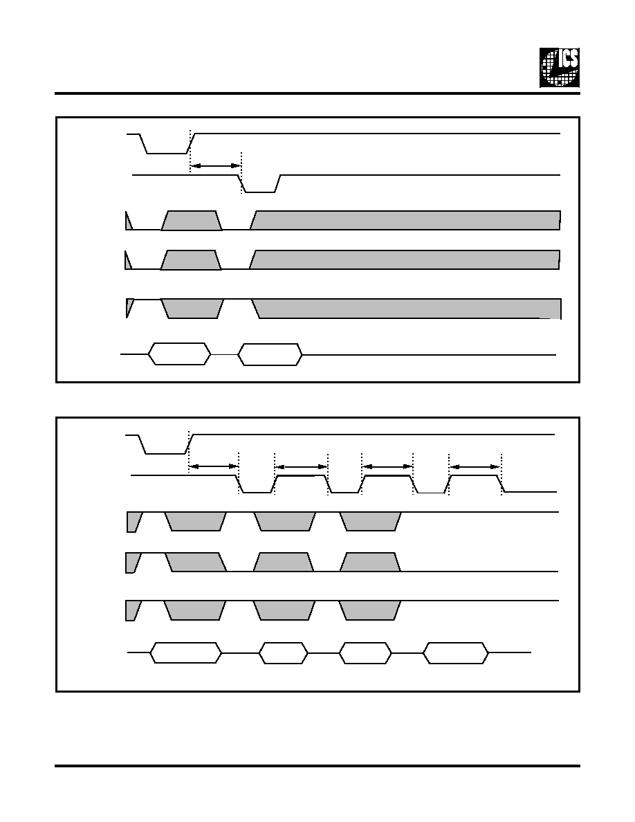
System Timing - Pseudo Color, Mode 0
Detailed Timing Specifications � Pseudo Color, Mode 0
PCLK
5342_8
BLANK
P0-P7
RED
GREEN
BLUE
A
B
C
D
E
F
G
H
I
J
K
A
F
F
F
G
G
G
B
C
C
C
B
B
A
A
BLANK
BLANK
BLANK
E
F
G
H
I
J
K
A
A
A
B
B
B
C
C
C
BLANK
BLANK
BLANK
F
F
F
G
G
G
t
PVCH
PLCK
BLANK
RED
BLUE
t
CHAV
t
CHAV
t
CHAV
t
CHBX
t
BVCH
t
CLPX
t
CHCL
t
CHCH
t
CLCH
5342_09
ICS5342
GENDAC
22
System Timing Bypass- 15(5/6/5) Modes 1,2
System Timing Bypass True Color 24 (8,8,8) Mode 3
PCLK
1
LOW BYTE
A
HIGH BYTE
A
LOW BYTE
B
HIGH BYTE
B
5342_10
2
3
4
A
B
B
B
A
A
5
6
7
BLANK
P0-P7
DAC-RD
DAC-GR
DAC-BL
PCLK
1
25ns
0ns
50ns
75ns
100ns
125ns
5342_11
150ns
2
3
4
5
6
7
8
9
A
A
BL
GR
RD
BL
GR
RD
B
B
C
C
BLANK
P0-P7
DAC-BL
DAC-GR
DAC-RD
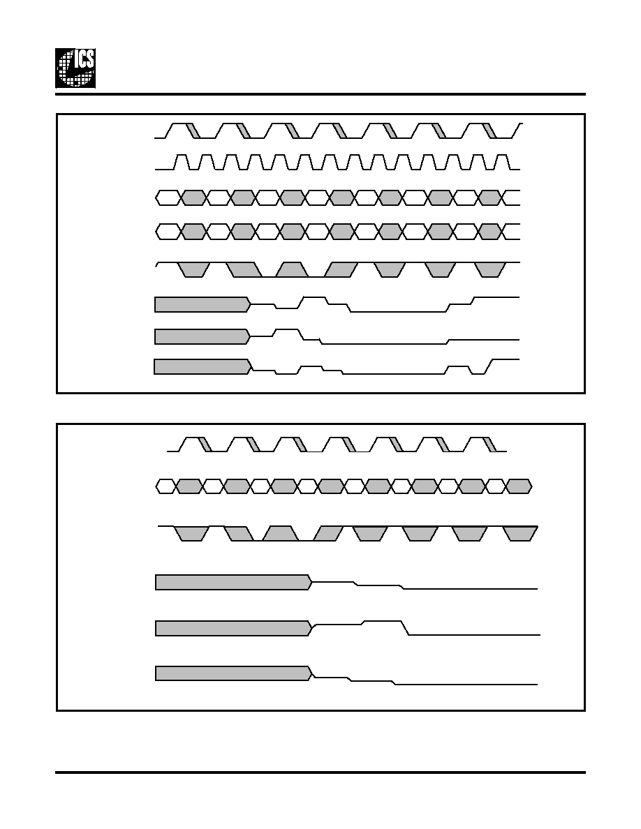
ICS5342
GENDAC
23
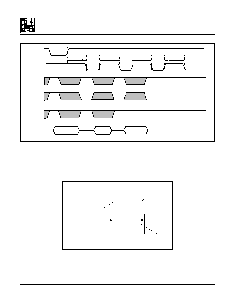
System Timing - 8-bit Pseudo Color, Mode 4
System Timing - 16-bit Color, Mode 5(5,5,5) and 6((5,6,5)
1
1
1
5342_12
A
A
C
E
G
J
L
N
B
D
F
H
K
M
P
K
K
L
J
J
J
L
L
B
C
C
C
D
D
D
B
B
A
A
BLANK
BLANK
BLANK
PCLK
ICLK
BLANK
P0-P7
P8-P15
RED
GREEN
BLUE
1
1
1
1
PCLK
5342_13
BLANK
P0-P7
RED
GREEN
BLUE
1
A
A
A
A
B
B
B
B
BLANK
BLANK
BLANK
C
D
E
F
G
H
2
3
4
5
6
7
ICS5342
GENDAC
24
System Timing - 16-bit Direct True Color, Mode 7
System Timing - 24-bit Packed Color, Mode 8
PCLK
5342_14
BLANK
P0-P7
RED
GREEN
BLUE
1
Ab
Ag
Ar
--
Bb
Bg
Br
--
Cb
Cg
Cr
--
Db
Dg
Dr
--
A
A
A
BLANK
BLANK
BLANK
2
3
4
5
6
7
PCLK
5342_15
BLANK
P0-P7
RED
GREEN
BLUE
1
AL
AM
AU
BL
BM
BU
CL
CM
CU
DL
DM
DU
EL
EM
EU
FL
FM
FU
GL
GM
A
B
B
B
A
A
BLANK
BLANK
BLANK
BLANK
BLANK
BLANK
2
3
4
5
6
7
ICS5342
GENDAC
25
Read-Write Timing
Basic Write Cycle Timing
t
WLWH
t
SVWL
t
WLSX
t
DVWH
t
WHDX
t
RLRH
t
SVRL
t
RLSX
t
RLQV
t
RHQX
t
RLQX
t
RHQZ
Basic Read Cycle Timing
5342_16
RS0-RS1
D0-D7
RD*
WR*
RS0-RS1
D0-D7
WR*
RD*
RS0
WR*
RD*
Write to Pixel Mask Register Followed by Write
Write to Pixel Mask Register Followed by Read
Read from Pixel or Pixel Address Register
(Read or Write) followed by Read
5342_17
RS1
t
WHWL1
t
WHRL1
Read from Pixel or Pixel Address Register
(Read or Write) followed by Write
t
RHRL1
t
RHWL1
ICS5342
GENDAC
26
Write and Read Back Pixel Address Register (Read Mode)
Write and Read Back Pixel Address Register (Write Mode)
W it
d R
d B
k Pi
l Add
R
i t
(R
d M d )
5342_18
RS0
RS1
RS2
D0-D7
WR*
RD*
t
WHRL1
ADDRESS
ADDRESS+1
5342_19
RS0
RS1
RS2
D0-D7
WR*
RD*
t
WHRL3
ADDRESS
ADDRESS
ICS5342
GENDAC
27
Read Color Value then Pixel Address Register (Read Mode)
Color Value Write Followed by any Read
5342_20
RS0
RS1
RS2
D0-D7
WR*
RD*
t
WHRL3
t
RHRL1
t
RHRL1
t
RHRL2
ADDRESS
GREEN
RED
BLUE
ADDRESS+2
WR*
RD*
t
WHWL1
t
WHWL1
t
WHWL1
t
WHRL2
5342_21
RS1
RS2
D0-D7
ADDRESS
GREEN
RED
BLUE
RS0
ICS5342
GENDAC
28
Color Value Write Followed by any Write
Color Value Read Followed by any Read
5342_22
RS0
RS1
RS2
D0-D7
WR*
RD*
t
WHWL1
t
WHWL1
t
WHWL1
t
WHWL2
ADDRESS
GREEN
RED
BLUE
5342_23
RS0
RS1
RS2
D0-D7
WR*
RD*
t
WHRL3
t
RHRL1
t
RHRL1
t
RHRL2
ADDRESS
GREEN
RED
BLUE
ICS5342
GENDAC
29
Color Value Read Followed by any Write
Write and Read back PLL Address Register (Write Mode)
5342_24
RS0
RS1
RS2
D0-D7
WR*
RD*
t
WHRL3
t
RHRL1
t
RHRL1
t
RHWL2
ADDRESS
GREEN
RED
BLUE
5342_25
RS0
RS1
RS2
D0-D7
WR*
RD*
t
WHRL3
ADDRESS
ADDRESS
ICS5342
GENDAC
30
Write and Read back PLL Address Register (Read Mode)
Read Two bytes PLL Register then PLL Address Register
5342_26
RS0
RS1
RS2
D0-D7
WR*
RD*
t
WHRL3
ADDRESS
ADDRESS+1
R
d T
B t
PLL R
i t
th
PLL Add
R
i t
5342_27
RS0
RS1
RS2
D0-D7
WR*
RD*
t
WHRL3
t
RHRL1
t
RHRL1
t
RHRL2
PLL ADDRESS
PLL HIGH
PLL LOW
ADR+1
ICS5342
GENDAC
31
Read One Byte PLL Register then PLL Address Register
Monitor SENSE Signal
5342_28
RS0
RS1
RS2
D0-D7
WR*
RD*
t
WHRL3
t
RHRL1
t
RHRL1
t
RHRL2
ADDRESS
PLL
ADR+1
RED
GREEN
BLUE
SENSE
0.335V
t
S0D
5342_29
ICS5342
GENDAC
32
Recommended Layout
VIA to power plane
VIA to ground plane
AGND
RED
AVDD
CVDD
GRN
BLUE
RSET
DVDD
PCLK
XVDD
XGND
XOUT
XIN
CLK0
36
35
34
33
32
31
30
29
28
27
40
39
38
37
43
42
41
60
59
58
57
56
55
54
53
52
51
50
49
48
47
46
45
44
1
2
3
4
5
6
7
8
9
68
64
65
66
67
61
62
63
GENDAC II
ICS5342
CLK1
DGND
10
11
12
13
14
15
16
17
18
19
20
21
22
23
24
25
26
R4
R2
R2
R4
R5
R1
C2
C2
VAA
C1
FB1
C3
-
-
+
C1 0.047
�
F chip capacitor
C2 0.1
�
F chip capacitor
C3 10
�
F tantalum capacitor
FB1 ferrite bead, Fair-Rite 2743019447
R1 33 ohm
R2 100 ohm
R3 141 ohm, 1%
R4 220 ohm
R5 560 ohm
Y1 parallel resonant crystal cut for C
L
= 12 pF
C2
LOCATE NEAR
CONTROLLER
LOCATE NEAR
CONTROLLER
C1
C2
R3
VAA
C2
Y1
VAA
C2
VREF
CGND
DGND
CVDD
CGND
5342_30
Board Layout and Analog Signal Consider-
ations
The high performance of the GENDAC is dependent on care-
ful PC board layout. The use of a four layer board (internal
power and ground planes, signals on the two surface layers) is
recommended. The ground plane layer should be closest to the
component side of the board. The layout following this sec-
tion shows a suggested configuration.
Power Supply
As a high speed CMOS device, the GENDAC may draw large
transient currents from the power supply. It is necessary to
adopt high-frequency board-layout and power-distribution
techniques to assure proper operation of the GENDAC. This
will also minimize radio frequency interference (RFI). DAC
to DAC crosstalk can also be attributed to a high impedance
power supply.

ICS5342
GENDAC
33
Note the power plane is not separated into analog and digital
supply regions. The power and ground planes are continuous,
not split. Power is supplied to the analog power pins through
the ferrite bead, and bypassed at the power entry point by C3,
a 10
�
F tantalum capacitor. Analog power connections should
be routed as shown in the diagram. They may be routed on the
back side so the analog signals are routed without vias. Power
pins 9 and 43 should be connected to digital power. Power
pins 27, 41 and 50 are connected to analog power (VAA). Ce-
ramic decoupling capacitors (indicated by C1 and C2) should
be placed as close to the GENDAC as possible. The power
traces should be routed through the capacitor pads and the
ground vias should not be shared. The rule is: one pad, one
via. The GENDAC analog ground pins should have multiple
vias to the ground plane, if possible.
To supply the transient currents required, the impedance in
the decoupling path should be kept to a minimum. It is just as
important that the connection between the capacitor ground
pad and the ground plane be short and direct. It is recommend-
ed that the decoupling capacitance between V
DD
and GND
should be a 0.047
�
F to 0.1
�
F high frequency capacitor. Chip
capacitors have the lowest lead inductance and are highly rec-
ommended. 0.047
�
F chip capacitors are more effective at fre-
quencies above 80 MHz than other values in the range of
0.022
�
F to 0.1
�
F. All supply pins must have a ceramic ca-
pacitor connected. A tantalum capacitor with a value between
10
�
F and 22
�
F is recommended to decouple low frequen-
cies. To further reduce power-supply noise, a ferrite bead may
be added in series with the positive supply to form a low pass
filter, as shown in the layout example. Power and ground trac-
es to the GENDAC should be 50 mils wide whenever possi-
ble.
Analog Signals
All analog and digital I/O lines are not shown. Analog signals
(DAC outputs, V
REF
, R
SET
) should only be routed on the top
side of the board. DAC output termination resistors should be
located as close as possible to the GENDAC for best signal
quality. Doing this will also reduce RFI.
Digital Input Information
To minimize differential ground noise between components
on the board, the impedance in the ground supply between the
GENDAC and the digital devices driving it should be mini-
mized. This or a high impedance ground trace on the control-
ler may cause false signals to the GENDAC. This can appear
as glitches on edge sensitive inputs such as RD*, WR*, and
STRB. Splitting the ground plane exacerbates this problem.
The combination of series impedance in the ground supply to
the GENDAC and transients in the current drawn by the de-
vice, will appear as voltage differences across the GND pins
on the GENDAC. The effect this will have is to compromise
the low time and duty cycle of the output clocks.
The PCB traces between the outputs of the TTL devices driv-
ing the GENDAC and the input to the GENDAC behave like
low impedance transmission lines. The trace is driven from a
low impedance source and terminated with a high impedance.
In accordance with transmission line principles, signal transi-
tions will be reflected from the high impedance input to the
device. Similarly, signal transitions will be inverted and re-
flected from the low impedance TTL output. Termination is
necessary to reduce or eliminate ringing; particularly the un-
dershoot caused by reflections. Termination may either be se-
ries or parallel. Series and parallel termination is the
recommended technique to use. This is accomplished by plac-
ing a resistor in series with the signal at the output of the clock
driver. The resistor matches the output buffer impedance to
that of the transmission line. At the far end of the line another
resistor is added to terminate the transmission line to VCC.
To minimize reflections, some experimentation is necessary
to find the proper value to use for the series termination. Gen-
erally, a series resistor with a value around 75
, and a parallel
resistor of 330
will be satisfactory. Since each design will
result in a different trace impedance, a resistor of a predeter-
mined value may not properly match the signal path imped-
ance. The proper value of resistance should be found
empirically.

ICS5342
GENDAC
34

ICS5342
GENDAC
35
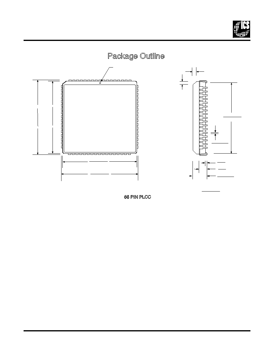
ICS5342
GENDAC
36
Package Detail
0.890 - 0.930
(22.61 - 23.62)
0.165 - 0.180
(4.20 - 4.57)
0.102
(2.59)
0.020
(0.51)
0.013 - 0.021
(0.33 - 0.53)
0.045
0.045
INCHES
(MILLIMETERS)
LEAD PITCH 0.050 TYPICAL
DIMENSIONS:
Package Outline
27
43
9
GENDAC II
ICS5342
61
0.985 - 0.995
(25.02 - 25.27)
0.950 - 0.958
(24.13 - 24.33)
0.985 - 0.995
(25.02 - 25.27)
0.950 - 0.958
(24.13 - 24.33)
PIN 1 IDENTIFIER
68 PIN PLCC
5342_31