Document Outline
- General Description
- Features
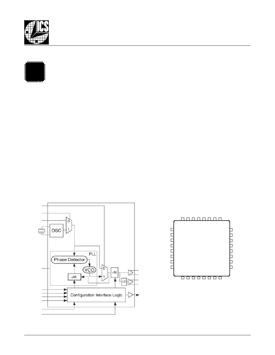
- Block Diagram
- Pin Assignment
- Functional Description
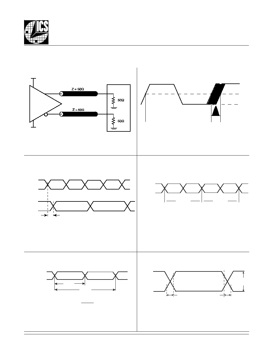
- Parallel & Serial Load Operations Diagram
- Pin Descriptions
- Pin Characteristics
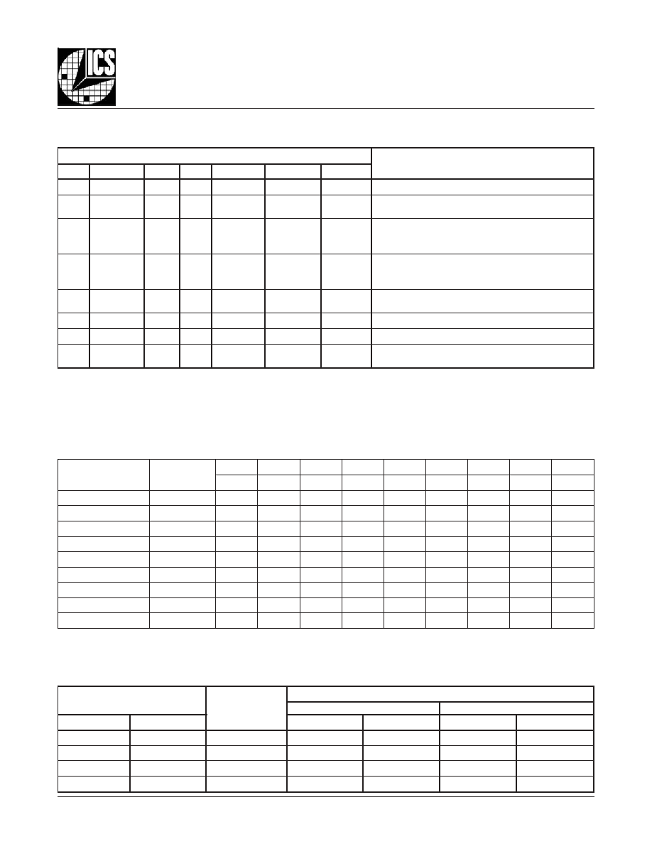
- Parallel & Serial Mode Function Table
- Programmable VCO Frequency Function Table
- Programmable Output Divider Function Table
- Absolute Maximum Ratings
- Power Supply DC Characteristics
- LVCMOS DC Characteristics
- LVPECL DC Characteristics
- Input Frequency Characteristics
- Crystal Characteristics
- AC Characteristics
- Parameter Measurement Information
- Applications
- Storage Area Networks
- Common SANs Appliations Frequencies
- Configuration Detials for SANs Applications
- Power Supply Filtering Techniques
- Termination for LVPECL Outputs
- Layout Guideline
- Power Considerations
- Power Dissipation
- Junction Temperature
- Thermal Resistance
- Calculations & Equations
- LVPECL Driver Circuit & Termination Diagram
- Reliability Information
- Transistor Count
- Package Outline
- Package Dimensions
- Ordering Information
8432CY-11
www.icst.com/products/hiperclocks.html
REV. E MAY 20, 2005
1
PRELIMINARY
Integrated
Circuit
Systems, Inc.
ICS8432-11
700MH
Z
/350MH
Z
, L
OW
P
HASE
N
OISE
,
C
RYSTAL
-
TO
- 3.3V LVPECL F
REQUENCY
S
YNTHESIZER
G
ENERAL
D
ESCRIPTION
The ICS8432-11 is a general purpose, dual output
Crystal-to-3.3V Differential LVPECL High Frequency
Synthesizer and a member of the HiPerClockSTM
family of High Performance Clock Solutions from
ICS. The ICS8432-11 has a selectable TEST_CLK
or crystal inputs. The TEST_CLK input accepts LVCMOS or
LVTTL input levels and translates them to 3.3V LVPECL
levels. The VCO operates at a frequency range of 200MHz
to 700MHz. The VCO frequency is programmed in steps
equal to the value of the input reference or crystal frequency.
Output frequencies up to 700MHz for FOUT and 350MHz
for FOUT/2 can be programmed using the serial or parallel
interfaces to the configuration logic. The low phase noise
characteristics and the multiple frequency outputs of the
ICS8432-11 makes it an ideal clock source for Fiber Channel
1 and 2, and Infiniband applications.
B
LOCK
D
IAGRAM
P
IN
A
SSIGNMENT
F
EATURES
∑ Dual differential 3.3V LVPECL outputs
∑ Selectable crystal oscillator interface or
LVCMOS/LVTTL TEST_CLK
∑ TEST_CLK can accept the following input levels:
LVCMOS or LVTTL
∑ Maximum FOUT frequency: 700MHz
∑ Maximum FOUT/2 frequency: 350MHz
∑ VCO range: 200MHz to 700MHz
∑ Parallel interface for programming counter and
VCO frequency multiplier and dividers
∑ Cycle-to-cycle jitter: 25ps (maximum)
∑ RMS period jitter: TBD
∑ 3.3V supply voltage
∑ 0∞C to 70∞C ambient operating temperature
32-Lead LQFP
7mm x 7mm x 1.4mm package body
Y Package
Top View
The Preliminary Information presented herein represents a product in prototyping or pre-production. The noted characteristics are based on initial
product characterization. Integrated Circuit Systems, Incorporated (ICS) reserves the right to change any circuitry or specifications without notice.
HiPerClockSTM
ICS
32 31 30 29 28 27 26 25
9 10 11 12 13 14 15 16
1
2
3
4
5
6
7
8
24
23
22
21
20
19
18
17
XTAL_IN
TEST_CLK
XTAL_SEL
V
CCA
S_LOAD
S_DATA
S_CLOCK
MR
M5
M6
M7
M8
N 0
N 1
nc
V
EE
V
EE
nFOUT
FOUT
V
CCO
nFOUT/2
FOUT/2
V
CC
TEST
XT
AL_OUT
nP_LOAD
VCO_SEL
M0
M1
M2
M3
M4
ICS8432-11
VCO_SEL
XTAL_SEL
TEST_CLK
XTAL_IN
XTAL_OUT
S_LOAD
S_DATA
S_CLOCK
nP_LOAD
M0:M8
N0:N1
FOUT
nFOUT
FOUT/2
nFOUT/2
TEST
MR
8432CY-11
www.icst.com/products/hiperclocks.html
REV. E MAY 20, 2005
2
PRELIMINARY
Integrated
Circuit
Systems, Inc.
ICS8432-11
700MH
Z
/350MH
Z
, L
OW
P
HASE
N
OISE
,
C
RYSTAL
-
TO
- 3.3V LVPECL F
REQUENCY
S
YNTHESIZER
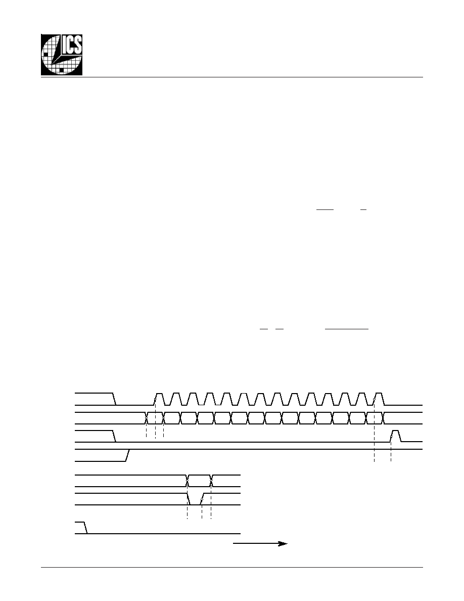
nP_LOAD or until a serial event occurs. As a result, the M and
N bits can be hardwired to set the M divider and N output divider
to a specific default state that will automatically occur during
power-up. The TEST output is LOW when operating in the paral-
lel input mode. The relationship between the VCO frequency,
the input frequency and the M divider is defined as follows:
The M value and the required values of M0 through M8 are
shown in Table 3B, Programmable VCO Frequency Function
Table. Valid M values for which the PLL will achieve lock are
defined as 8
M 28. The frequency out is defined as follows:
Serial operation occurs when nP_LOAD is HIGH and S_LOAD
is LOW. The shift register is loaded by sampling the S_DATA
bits with the rising edge of S_CLOCK. The contents of the
shift register are loaded into the M divider and N output
divider when S_LOAD transitions from LOW-to-HIGH. The
M divide and N output divide values are latched on the HIGH-
to-LOW transition of S_LOAD. If S_LOAD is held HIGH, data
at the S_DATA input is passed directly to the M divider and
N output divider on each rising edge of S_CLOCK. The serial
mode can be used to program the M and N bits and test bits
T1 and T0. The internal registers T0 and T1 determine the state
of the TEST output as follows:
Time
S
ERIAL
L
OADING
P
ARALLEL
L
OADING
M, N
F
UNCTIONAL
D
ESCRIPTION
NOTE: The functional description that follows describes
operation using a 25MHz clock input. Valid PLL loop divider
values for different input frequencies are defined in the Input
Frequency Characteristics, Table 5, NOTE 1.
The ICS8432-11 features a fully integrated PLL and there-
fore requires no external components for setting the loop
bandwidth. A differential clock input is used as the input to the
ICS8432-11. This input is fed into the phase detector. A 25MHz
clock input provides a 25MHz phase detector reference fre-
quency. The VCO of the PLL operates over a range of 200MHz
to 700MHz. The output of the M divider is also applied to the
phase detector.
The phase detector and the M divider force the VCO output
frequency to be M times the reference frequency by adjust-
ing the VCO control voltage. Note, that for some values of M
(either too high or too low), the PLL will not achieve lock. The
output of the VCO is scaled by a divider prior to being sent
to each of the LVPECL output buffers. The divider provides
a 50% output duty cycle.
The programmable features of the ICS8432-11 support two
input modes to program the PLL M divider and N output
divider. The two input operational modes are parallel and
serial. Figure1 shows the timing diagram for each mode. In
parallel mode, the nP_LOAD input is initially LOW. The data
on inputs M0 through M8 and N0 and N1 is passed directly
to the M divider and N output divider. On the LOW-to-HIGH
transition of the nP_LOAD input, the data is latched and the
M divider remains loaded until the next LOW transition on
fVCO = fxtal x M
T1
T0
TEST Output
0
0
LOW
0
1
S_Data, Shift Register Input
1
0
Output of M divider
1
1
CMOS Fout/2
F
IGURE
1. P
ARALLEL
& S
ERIAL
L
OAD
O
PERATIONS
*NOTE:
The NULL timing slot must be observed.
T1
T0
*
NULL
N 1
N 0
M8
M7
M6
M5
M4
M3
M2
M1
M0
S_CLOCK
S_DATA
S_LOAD
nP_LOAD
M0:M8, N0:N1
nP_LOAD
S_LOAD
fOUT = fVCO = fxtal x M
N
N

8432CY-11
www.icst.com/products/hiperclocks.html
REV. E MAY 20, 2005
3
PRELIMINARY
Integrated
Circuit
Systems, Inc.
ICS8432-11
700MH
Z
/350MH
Z
, L
OW
P
HASE
N
OISE
,
C
RYSTAL
-
TO
- 3.3V LVPECL F
REQUENCY
S
YNTHESIZER
T
ABLE
1. P
IN
D
ESCRIPTIONS
r
e
b
m
u
N
e
m
a
N
e
p
y
T
n
o
i
t
p
i
r
c
s
e
D
1
5
M
t
u
p
n
I
p
u
ll
u
P
f
o
n
o
i
t
s
i
s
n
a
r
t
H
G
I
H
-
o
t
-
W
O
L
n
o
d
e
h
c
t
a
l
a
t
a
D
.
s
t
u
p
n
i
r
e
d
i
v
i
d
M
.
s
l
e
v
e
l
e
c
a
f
r
e
t
n
i
L
T
T
V
L
/
S
O
M
C
V
L
.
t
u
p
n
i
D
A
O
L
_
P
n
,
4
,
3
,
2
,
9
2
,
8
2
2
3
,
1
3
,
0
3
,
8
M
,
7
M
,
6
M
,
1
M
,
0
M
4
M
,
3
M
,
2
M
t
u
p
n
I
n
w
o
d
ll
u
P
6
,
5
1
N
,
0
N
t
u
p
n
I
n
w
o
d
ll
u
P
C
3
e
l
b
a
T
n
i
d
e
n
i
f
e
d
s
a
e
u
l
a
v
r
e
d
i
v
i
d
t
u
p
t
u
o
N
s
e
n
i
m
r
e
t
e
D
.
s
l
e
v
e
l
e
c
a
f
r
e
t
n
i
L
T
T
V
L
/
S
O
M
C
V
L
.
e
l
b
a
T
n
o
i
t
c
n
u
F
7
c
n
d
e
s
u
n
U
.
t
c
e
n
n
o
c
o
N
6
1
,
8
V
E
E
r
e
w
o
P
.
s
n
i
p
y
l
p
p
u
s
e
v
i
t
a
g
e
N
9
T
S
E
T
t
u
p
t
u
O
.
n
o
i
t
a
r
e
p
o
f
o
e
d
o
m
l
a
i
r
e
s
e
h
t
n
i
E
V
I
T
C
A
s
i
h
c
i
h
w
t
u
p
t
u
o
t
s
e
T
.
s
l
e
v
e
l
e
c
a
f
r
e
t
n
i
S
O
M
C
V
L
.
e
d
o
m
l
e
ll
a
r
a
p
n
i
W
O
L
n
e
v
i
r
d
t
u
p
t
u
O
0
1
V
C
C
r
e
w
o
P
.
n
i
p
y
l
p
p
u
s
e
r
o
C
2
1
,
1
1
2
/
T
U
O
F
n
,
2
/
T
U
O
F
t
u
p
t
u
O
.
r
e
z
i
s
e
h
t
n
y
s
e
h
t
r
o
f
t
u
p
t
u
o
l
a
i
t
n
e
r
e
f
f
i
d
y
c
n
e
u
q
e
r
f
f
l
a
H
.
s
l
e
v
e
l
e
c
a
f
r
e
t
n
i
L
C
E
P
V
L
V
3
.
3
3
1
V
O
C
C
r
e
w
o
P
.
n
i
p
y
l
p
p
u
s
t
u
p
t
u
O
5
1
,
4
1
T
U
O
F
n
,
T
U
O
F
t
u
p
t
u
O
.
r
e
z
i
s
e
h
t
n
y
s
e
h
t
r
o
f
t
u
p
t
u
o
l
a
i
t
n
e
r
e
f
f
i
D
.
s
l
e
v
e
l
e
c
a
f
r
e
t
n
i
L
C
E
P
V
L
V
3
.
3
7
1
R
M
t
u
p
n
I
n
w
o
d
ll
u
P
s
r
e
d
i
v
i
d
l
a
n
r
e
t
n
i
e
h
t
,
H
G
I
H
c
i
g
o
l
n
e
h
W
.
t
e
s
e
R
r
e
t
s
a
M
h
g
i
H
e
v
i
t
c
A
e
h
t
d
n
a
w
o
l
o
g
o
t
)
x
T
U
O
F
(
s
t
u
p
t
u
o
e
u
r
t
e
h
t
g
n
i
s
u
a
c
t
e
s
r
e
r
a
e
h
t
,
W
O
L
c
i
g
o
l
n
e
h
W
.
h
g
i
h
o
g
o
t
)
x
T
U
O
F
n
(
s
t
u
p
t
u
o
d
e
t
r
e
v
n
i
R
M
f
o
n
o
i
t
r
e
s
s
A
.
d
e
l
b
a
n
e
e
r
a
s
t
u
p
t
u
o
e
h
t
d
n
a
s
r
e
d
i
v
i
d
l
a
n
r
e
t
n
i
.
s
e
u
l
a
v
T
d
n
a
,
N
,
M
d
e
d
a
o
l
t
c
e
f
f
a
t
o
n
s
e
o
d
.
s
l
e
v
e
l
e
c
a
f
r
e
t
n
i
L
T
T
V
L
/
S
O
M
C
V
L
8
1
K
C
O
L
C
_
S
t
u
p
n
I
n
w
o
d
ll
u
P
r
e
t
s
i
g
e
r
t
f
i
h
s
e
h
t
o
t
n
i
t
u
p
n
i
A
T
A
D
_
S
t
a
t
n
e
s
e
r
p
a
t
a
d
l
a
i
r
e
s
n
i
s
k
c
o
l
C
.
K
C
O
L
C
_
S
f
o
e
g
d
e
g
n
i
s
i
r
e
h
t
n
o
.
s
l
e
v
e
l
e
c
a
f
r
e
t
n
i
L
T
T
V
L
/
S
O
M
C
V
L
9
1
A
T
A
D
_
S
t
u
p
n
I
n
w
o
d
ll
u
P
f
o
e
g
d
e
g
n
i
s
i
r
e
h
t
n
o
d
e
l
p
m
a
s
a
t
a
D
.
t
u
p
n
i
l
a
i
r
e
s
r
e
t
s
i
g
e
r
t
f
i
h
S
.
s
l
e
v
e
l
e
c
a
f
r
e
t
n
i
L
T
T
V
L
/
S
O
M
C
V
L
.
K
C
O
L
C
_
S
0
2
D
A
O
L
_
S
t
u
p
n
I
n
w
o
d
ll
u
P
.
s
r
e
d
i
v
i
d
e
h
t
o
t
n
i
r
e
t
s
i
g
e
r
t
f
i
h
s
m
o
r
f
a
t
a
d
f
o
n
o
i
t
i
s
n
a
r
t
s
l
o
r
t
n
o
C
.
s
l
e
v
e
l
e
c
a
f
r
e
t
n
i
L
T
T
V
L
/
S
O
M
C
V
L
1
2
V
A
C
C
r
e
w
o
P
.
n
i
p
y
l
p
p
u
s
g
o
l
a
n
A
2
2
L
E
S
_
L
A
T
X
t
u
p
n
I
p
u
ll
u
P
e
c
n
e
r
e
f
e
r
L
L
P
e
h
t
s
a
s
t
u
p
n
i
t
s
e
t
r
o
l
a
t
s
y
r
c
n
e
e
w
t
e
b
s
t
c
e
l
e
S
s
t
u
p
n
i
L
A
T
X
s
t
c
e
l
e
S
.
s
l
e
v
e
l
e
c
a
f
r
e
t
n
i
L
T
T
V
L
/
S
O
M
C
V
L
.
e
c
r
u
o
s
.
W
O
L
n
e
h
w
K
L
C
_
T
S
E
T
s
t
c
e
l
e
S
.
H
G
I
H
n
e
h
w
3
2
K
L
C
_
T
S
E
T
t
u
p
n
I
n
w
o
d
ll
u
P
.
s
l
e
v
e
l
e
c
a
f
r
e
t
n
i
L
T
T
V
L
/
S
O
M
C
V
L
.
t
u
p
n
i
k
c
o
l
c
t
s
e
T
,
4
2
5
2
,
N
I
_
L
A
T
X
T
U
O
_
L
A
T
X
t
u
p
n
I
.
t
u
p
n
i
e
h
t
s
i
N
I
_
L
A
T
X
.
s
t
u
p
n
i
r
o
t
a
ll
i
c
s
o
l
a
t
s
y
r
C
.
t
u
p
t
u
o
e
h
t
s
i
T
U
O
_
L
A
T
X
6
2
D
A
O
L
_
P
n
t
u
p
n
I
n
w
o
d
ll
u
P
s
i
0
M
:
8
M
t
a
t
n
e
s
e
r
p
a
t
a
d
n
e
h
w
s
e
n
i
m
r
e
t
e
D
.
t
u
p
n
i
d
a
o
l
l
e
ll
a
r
a
P
e
h
t
s
t
e
s
0
N
:
1
N
t
a
t
n
e
s
e
r
p
a
t
a
d
n
e
h
w
d
n
a
,
r
e
d
i
v
i
d
M
o
t
n
i
d
e
d
a
o
l
.
s
l
e
v
e
l
e
c
a
f
r
e
t
n
i
L
T
T
V
L
/
S
O
M
C
V
L
.
e
u
l
a
v
r
e
d
i
v
i
d
t
u
p
t
u
o
N
7
2
L
E
S
_
O
C
V
t
u
p
n
I
p
u
ll
u
P
.
e
d
o
m
s
s
a
p
y
b
r
o
L
L
P
n
i
s
i
r
e
z
i
s
e
h
t
n
y
s
r
e
h
t
e
h
w
s
e
n
i
m
r
e
t
e
D
.
s
l
e
v
e
l
e
c
a
f
r
e
t
n
i
L
T
T
V
L
/
S
O
M
C
V
L
.
s
e
u
l
a
v
l
a
c
i
p
y
t
r
o
f
,
s
c
i
t
s
i
r
e
t
c
a
r
a
h
C
n
i
P
,
2
e
l
b
a
T
e
e
S
.
s
r
o
t
s
i
s
e
r
t
u
p
n
i
l
a
n
r
e
t
n
i
o
t
r
e
f
e
r
n
w
o
d
ll
u
P
d
n
a
p
u
ll
u
P
:
E
T
O
N
T
ABLE
2. P
IN
C
HARACTERISTICS
l
o
b
m
y
S
r
e
t
e
m
a
r
a
P
s
n
o
i
t
i
d
n
o
C
t
s
e
T
m
u
m
i
n
i
M
l
a
c
i
p
y
T
m
u
m
i
x
a
M
s
t
i
n
U
C
N
I
e
c
n
a
t
i
c
a
p
a
C
t
u
p
n
I
4
F
p
R
P
U
L
L
U
P
r
o
t
s
i
s
e
R
p
u
ll
u
P
t
u
p
n
I
1
5
k
R
N
W
O
D
L
L
U
P
r
o
t
s
i
s
e
R
n
w
o
d
ll
u
P
t
u
p
n
I
1
5
k
8432CY-11
www.icst.com/products/hiperclocks.html
REV. E MAY 20, 2005
4
PRELIMINARY
Integrated
Circuit
Systems, Inc.
ICS8432-11
700MH
Z
/350MH
Z
, L
OW
P
HASE
N
OISE
,
C
RYSTAL
-
TO
- 3.3V LVPECL F
REQUENCY
S
YNTHESIZER
T
ABLE
3A. P
ARALLEL
AND
S
ERIAL
M
ODES
F
UNCTION
T
ABLE
s
t
u
p
n
I
s
n
o
i
t
i
d
n
o
C
R
M
D
A
O
L
_
P
n
M
N
D
A
O
L
_
S
K
C
O
L
C
_
S
A
T
A
D
_
S
H
X
X
X
X
X
X
.
t
e
s
e
r
s
r
e
t
n
u
o
c
N
d
n
a
M
.
t
e
s
e
R
L
L
a
t
a
D
a
t
a
D
X
X
X
e
h
t
o
t
y
l
t
c
e
r
i
d
d
e
s
s
a
p
s
t
u
p
n
i
N
d
n
a
M
n
o
a
t
a
D
.
W
O
L
d
e
c
r
o
f
t
u
p
t
u
o
T
S
E
T
.
r
e
d
i
v
i
d
M
L
a
t
a
D
a
t
a
D
L
X
X
s
n
i
a
m
e
r
d
n
a
s
r
e
t
s
i
g
e
r
t
u
p
n
i
o
t
n
i
d
e
h
c
t
a
l
s
i
a
t
a
D
l
a
i
r
e
s
a
li
t
n
u
r
o
n
o
i
t
i
s
n
a
r
t
W
O
L
t
x
e
n
li
t
n
u
d
e
d
a
o
l
.
s
r
u
c
c
o
t
n
e
v
e
L
H
X
X
L
a
t
a
D
h
t
i
w
d
e
d
a
o
l
s
i
r
e
t
s
i
g
e
r
t
f
i
h
S
.
e
d
o
m
t
u
p
n
i
l
a
i
r
e
S
f
o
e
g
d
e
g
n
i
s
i
r
h
c
a
e
n
o
A
T
A
D
_
S
n
o
a
t
a
d
.
K
C
O
L
C
_
S
L
H
X
X
L
a
t
a
D
e
h
t
o
t
d
e
s
s
a
p
e
r
a
r
e
t
s
i
g
e
r
t
f
i
h
s
e
h
t
f
o
s
t
n
e
t
n
o
C
.
r
e
d
i
v
i
d
M
L
H
X
X
L
a
t
a
D
.
d
e
h
c
t
a
l
e
r
a
s
e
u
l
a
v
r
e
d
i
v
i
d
t
u
p
t
u
o
N
d
n
a
r
e
d
i
v
i
d
M
L
H
X
X
L
X
X
.
s
r
e
t
s
i
g
e
r
t
f
i
h
s
t
c
e
f
f
a
t
o
n
o
d
t
u
p
n
i
l
a
i
r
e
s
r
o
l
e
ll
a
r
a
P
L
H
X
X
H
a
t
a
D
s
i
t
i
s
a
r
e
d
i
v
i
d
M
o
t
y
l
t
c
e
r
i
d
d
e
s
s
a
p
A
T
A
D
_
S
.
d
e
k
c
o
l
c
W
O
L
=
L
:
E
T
O
N
H
G
I
H
=
H
e
r
a
c
t
'
n
o
D
=
X
n
o
i
t
i
s
n
a
r
t
e
g
d
e
g
n
i
s
i
R
=
n
o
i
t
i
s
n
a
r
t
e
g
d
e
g
n
il
l
a
F
=
T
ABLE
3B. P
ROGRAMMABLE
VCO F
REQUENCY
F
UNCTION
T
ABLE
T
ABLE
3C. P
ROGRAMMABLE
O
UTPUT
D
IVIDER
F
UNCTION
T
ABLE
s
t
u
p
n
I
e
u
l
a
V
r
e
d
i
v
i
D
N
)
z
H
M
(
y
c
n
e
u
q
e
r
F
t
u
p
t
u
O
T
U
O
F
2
/
T
U
O
F
1
N
0
N
m
u
m
i
n
i
M
m
u
m
i
x
a
M
m
u
m
i
n
i
M
m
u
m
i
x
a
M
0
0
1
0
0
2
0
0
7
5
2
1
0
5
3
0
1
2
0
0
1
0
5
3
5
.
2
6
5
7
1
1
0
4
0
5
5
7
1
5
2
.
1
3
5
.
7
8
1
1
8
5
2
5
.
7
8
5
2
6
.
5
1
5
7
.
3
4
y
c
n
e
u
q
e
r
F
O
C
V
)
z
H
M
(
e
d
i
v
i
D
M
6
5
2
8
2
1
4
6
2
3
6
1
8
4
2
1
8
M
7
M
6
M
5
M
4
M
3
M
2
M
1
M
0
M
0
0
2
8
0
0
0
0
0
1
0
0
0
5
2
2
9
0
0
0
0
0
1
0
0
1
0
5
2
0
1
0
0
0
0
0
1
0
1
0
5
7
2
1
1
0
0
0
0
0
1
0
1
1
∑
∑
∑
∑
∑
∑
∑
∑
∑
∑
∑
∑
∑
∑
∑
∑
∑
∑
∑
∑
∑
∑
0
5
6
6
2
0
0
0
0
1
1
0
1
0
5
7
6
7
2
0
0
0
0
1
1
0
1
1
0
0
7
8
2
0
0
0
0
1
1
1
0
0
f
o
y
c
n
e
u
q
e
r
f
t
u
p
n
i
K
L
C
_
T
S
E
T
r
o
l
a
t
s
y
r
c
o
t
d
n
o
p
s
e
r
r
o
c
s
e
i
c
n
e
u
q
e
r
f
g
n
i
t
l
u
s
e
r
e
h
t
d
n
a
s
e
u
l
a
v
e
d
i
v
i
d
M
e
s
e
h
T
:
1
E
T
O
N
.
z
H
M
5
2
8432CY-11
www.icst.com/products/hiperclocks.html
REV. E MAY 20, 2005
5
PRELIMINARY
Integrated
Circuit
Systems, Inc.
ICS8432-11
700MH
Z
/350MH
Z
, L
OW
P
HASE
N
OISE
,
C
RYSTAL
-
TO
- 3.3V LVPECL F
REQUENCY
S
YNTHESIZER
T
ABLE
4A. P
OWER
S
UPPLY
DC C
HARACTERISTICS
,
V
CC
= V
CCA
= V
CCO
= 3.3V±5%, T
A
= 0∞C
TO
70∞C
l
o
b
m
y
S
r
e
t
e
m
a
r
a
P
s
n
o
i
t
i
d
n
o
C
t
s
e
T
m
u
m
i
n
i
M
l
a
c
i
p
y
T
m
u
m
i
x
a
M
s
t
i
n
U
V
C
C
e
g
a
t
l
o
V
y
l
p
p
u
S
e
v
i
t
i
s
o
P
5
3
1
.
3
3
.
3
5
6
4
.
3
V
V
A
C
C
e
g
a
t
l
o
V
y
l
p
p
u
S
g
o
l
a
n
A
5
3
1
.
3
3
.
3
5
6
4
.
3
V
V
O
C
C
e
g
a
t
l
o
V
y
l
p
p
u
S
t
u
p
t
u
O
5
3
1
.
3
3
.
3
5
6
4
.
3
V
I
E
E
t
n
e
r
r
u
C
y
l
p
p
u
S
r
e
w
o
P
0
1
1
A
m
I
A
C
C
t
n
e
r
r
u
C
y
l
p
p
u
S
g
o
l
a
n
A
5
1
A
m
T
ABLE
4B. LVCMOS / LVTTL DC C
HARACTERISTICS
,
V
CC
= V
CCA
= V
CCO
= 3.3V±5%, T
A
= 0∞C
TO
70∞C
NOTE 1: Outputs terminated with 50
to V
CCO
/2. See "Parameter Measurement Information" section,
"3.3V Output Load Test Circuit" figure.
l
o
b
m
y
S
r
e
t
e
m
a
r
a
P
s
n
o
i
t
i
d
n
o
C
t
s
e
T
m
u
m
i
n
i
M
l
a
c
i
p
y
T
m
u
m
i
x
a
M
s
t
i
n
U
V
H
I
e
g
a
t
l
o
V
h
g
i
H
t
u
p
n
I
2
V
C
C
3
.
0
+
V
V
L
I
e
g
a
t
l
o
V
w
o
L
t
u
p
n
I
3
.
0
-
8
.
0
V
I
H
I
t
u
p
n
I
t
n
e
r
r
u
C
h
g
i
H
,
R
M
,
1
N
,
0
N
,
8
M
-
6
M
,
4
M
-
0
M
,
K
L
C
_
T
S
E
T
,
K
C
O
L
C
_
S
D
A
O
L
_
P
n
,
D
A
O
L
_
S
,
A
T
A
D
_
S
V
C
C
V
=
N
I
V
5
6
4
.
3
=
0
5
1
A
µ
L
E
S
_
O
C
V
,
L
E
S
_
L
A
T
X
,
5
M
V
C
C
V
=
N
I
V
5
6
4
.
3
=
5
A
µ
I
L
I
t
u
p
n
I
t
n
e
r
r
u
C
w
o
L
,
R
M
,
1
N
,
0
N
,
8
M
-
6
M
,
4
M
-
0
M
,
K
L
C
_
T
S
E
T
,
K
C
O
L
C
_
S
D
A
O
L
_
P
n
,
D
A
O
L
_
S
,
A
T
A
D
_
S
V
C
C
,
V
5
6
4
.
3
=
V
N
I
V
0
=
5
-
A
µ
L
E
S
_
O
C
V
,
L
E
S
_
L
A
T
X
,
5
M
V
C
C
,
V
5
6
4
.
3
=
V
N
I
V
0
=
0
5
1
-
A
µ
V
H
O
t
u
p
t
u
O
e
g
a
t
l
o
V
h
g
i
H
1
E
T
O
N
;
T
S
E
T
6
.
2
V
V
L
O
t
u
p
t
u
O
e
g
a
t
l
o
V
w
o
L
1
E
T
O
N
;
T
S
E
T
5
.
0
V
A
BSOLUTE
M
AXIMUM
R
ATINGS
Supply Voltage, V
CC
4.6V
Inputs, V
I
-0.5V to V
CC
+ 0.5 V
Outputs, I
O
Continuous Current
50mA
Surge Current
100mA
Package Thermal Impedance,
JA
47.9∞C/W (0 lfpm)
Storage Temperature, T
STG
-65∞C to 150∞C
NOTE: Stresses beyond those listed under Absolute
Maximum Ratings may cause permanent damage to the
device. These ratings are stress specifications only. Functional
operation of product at these conditions or any conditions be-
yond those listed in the
DC Characteristics or AC Character-
istics is not implied. Exposure to absolute maximum rating
conditions for extended periods may affect product reliability.
8432CY-11
www.icst.com/products/hiperclocks.html
REV. E MAY 20, 2005
6
PRELIMINARY
Integrated
Circuit
Systems, Inc.
ICS8432-11
700MH
Z
/350MH
Z
, L
OW
P
HASE
N
OISE
,
C
RYSTAL
-
TO
- 3.3V LVPECL F
REQUENCY
S
YNTHESIZER
T
ABLE
7. AC C
HARACTERISTICS
,
V
CC
= V
CCA
= V
CCO
= 3.3V±5%, T
A
= 0∞C
TO
70∞C
l
o
b
m
y
S
r
e
t
e
m
a
r
a
P
s
n
o
i
t
i
d
n
o
C
t
s
e
T
m
u
m
i
n
i
M
l
a
c
i
p
y
T
m
u
m
i
x
a
M
s
t
i
n
U
F
T
U
O
y
c
n
e
u
q
e
r
F
t
u
p
t
u
O
5
2
0
0
7
z
H
M
)
c
c
(
t
ij
t
3
,
1
E
T
O
N
;
r
e
t
t
i
J
e
l
c
y
C
-
o
t
-
e
l
c
y
C
5
2
s
p
)
r
e
p
(
t
ij
t
3
,
1
E
T
O
N
;
S
M
R
,
r
e
t
t
i
J
d
o
i
r
e
P
D
B
T
s
p
t
)
o
(
k
s
3
,
2
E
T
O
N
;
w
e
k
S
t
u
p
t
u
O
D
B
T
s
p
t
R
e
m
i
T
e
s
i
R
t
u
p
t
u
O
z
H
M
0
5
@
%
0
8
o
t
%
0
2
0
0
3
0
0
7
s
p
t
F
e
m
i
T
ll
a
F
t
u
p
t
u
O
z
H
M
0
5
@
%
0
8
o
t
%
0
2
0
0
3
0
0
7
s
p
t
S
e
m
i
T
p
u
t
e
S
D
A
O
L
_
P
n
o
t
N
,
M
5
s
n
K
C
O
L
C
_
S
o
t
A
T
A
D
_
S
5
s
n
D
A
O
L
_
S
o
t
K
C
O
L
C
_
S
5
s
n
t
H
e
m
i
T
d
l
o
H
D
A
O
L
_
P
n
o
t
N
,
M
5
s
n
K
C
O
L
C
_
S
o
t
A
T
A
D
_
S
5
s
n
D
A
O
L
_
S
o
t
K
C
O
L
C
_
S
5
s
n
c
d
o
e
l
c
y
C
y
t
u
D
t
u
p
t
u
O
7
4
3
5
%
t
K
C
O
L
e
m
i
T
k
c
o
L
L
L
P
0
1
s
m
.
e
s
i
w
r
e
h
t
o
d
e
t
o
n
s
s
e
l
n
u
z
H
M
0
0
5
t
a
d
e
r
u
s
a
e
m
s
r
e
t
e
m
a
r
a
p
ll
A
.
s
t
u
p
n
i
L
A
T
X
g
n
i
s
u
e
c
n
a
m
r
o
f
r
e
p
r
e
t
t
i
J
:
1
E
T
O
N
.
s
n
o
i
t
i
d
n
o
c
d
a
o
l
l
a
u
q
e
h
t
i
w
d
n
a
e
g
a
t
l
o
v
y
l
p
p
u
s
e
m
a
s
e
h
t
t
a
s
t
u
p
t
u
o
n
e
e
w
t
e
b
w
e
k
s
s
a
d
e
n
i
f
e
D
:
2
E
T
O
N
.
s
t
n
i
o
p
s
s
o
r
c
l
a
i
t
n
e
r
e
f
f
i
d
t
u
p
t
u
o
e
h
t
t
a
d
e
r
u
s
a
e
M
.
5
6
d
r
a
d
n
a
t
S
C
E
D
E
J
h
t
i
w
e
c
n
a
d
r
o
c
c
a
n
i
d
e
n
i
f
e
d
s
i
r
e
t
e
m
a
r
a
p
s
i
h
T
:
3
E
T
O
N
T
ABLE
4C. LVPECL DC C
HARACTERISTICS
,
V
CC
= V
CCA
= V
CCO
= 3.3V±5%, T
A
= 0∞C
TO
70∞C
l
o
b
m
y
S
r
e
t
e
m
a
r
a
P
s
n
o
i
t
i
d
n
o
C
t
s
e
T
m
u
m
i
n
i
M
l
a
c
i
p
y
T
m
u
m
i
x
a
M
s
t
i
n
U
V
H
O
1
E
T
O
N
;
e
g
a
t
l
o
V
h
g
i
H
t
u
p
t
u
O
V
O
C
C
4
.
1
-
V
O
C
C
9
.
0
-
V
V
L
O
1
E
T
O
N
;
e
g
a
t
l
o
V
w
o
L
t
u
p
t
u
O
V
O
C
C
0
.
2
-
V
O
C
C
7
.
1
-
V
V
G
N
I
W
S
g
n
i
w
S
e
g
a
t
l
o
V
t
u
p
t
u
O
k
a
e
P
-
o
t
-
k
a
e
P
6
.
0
0
.
1
V
0
5
h
t
i
w
d
e
t
a
n
i
m
r
e
t
s
t
u
p
t
u
O
:
1
E
T
O
N
V
o
t
O
C
C
.
V
2
-
T
ABLE
5. I
NPUT
F
REQUENCY
C
HARACTERISTICS
,
V
CC
= V
CCA
= V
CCO
= 3.3V±5%, T
A
= 0∞C
TO
70∞C
l
o
b
m
y
S
r
e
t
e
m
a
r
a
P
s
n
o
i
t
i
d
n
o
C
t
s
e
T
m
u
m
i
n
i
M
l
a
c
i
p
y
T
m
u
m
i
x
a
M
s
t
i
n
U
f
N
I
y
c
n
e
u
q
e
r
F
t
u
p
n
I
1
E
T
O
N
;
K
L
C
_
T
S
E
T
2
1
5
2
z
H
M
;
T
U
O
_
L
A
T
X
,
N
I
_
L
A
T
X
1
E
T
O
N
2
1
5
2
z
H
M
K
C
O
L
C
_
S
D
B
T
z
H
M
e
h
t
n
i
h
t
i
w
e
t
a
r
e
p
o
o
t
O
C
V
e
h
t
r
o
f
t
e
s
e
b
t
s
u
m
e
u
l
a
v
M
e
h
t
,
e
g
n
a
r
y
c
n
e
u
q
e
r
f
K
L
C
_
T
S
E
T
d
n
a
l
a
t
s
y
r
c
t
u
p
n
i
e
h
t
r
o
F
:
1
E
T
O
N
7
1
e
r
a
M
f
o
s
e
u
l
a
v
d
il
a
v
,
z
H
M
2
1
f
o
y
c
n
e
u
q
e
r
f
t
u
p
n
i
m
u
m
i
n
i
m
e
h
t
g
n
i
s
U
.
e
g
n
a
r
z
H
M
0
0
7
o
t
z
H
M
0
0
2
M
e
h
t
g
n
i
s
U
.
8
5
8
e
r
a
M
f
o
s
e
u
l
a
v
d
il
a
v
,
z
H
M
5
2
f
o
y
c
n
e
u
q
e
r
f
m
u
m
i
x
a
m
M
.
8
2
T
ABLE
6. C
RYSTAL
C
HARACTERISTICS
r
e
t
e
m
a
r
a
P
s
n
o
i
t
i
d
n
o
C
t
s
e
T
m
u
m
i
n
i
M
l
a
c
i
p
y
T
m
u
m
i
x
a
M
s
t
i
n
U
n
o
i
t
a
ll
i
c
s
O
f
o
e
d
o
M
l
a
t
n
e
m
a
d
n
u
F
y
c
n
e
u
q
e
r
F
2
1
5
2
z
H
M
)
R
S
E
(
e
c
n
a
t
s
i
s
e
R
s
e
i
r
e
S
t
n
e
l
a
v
i
u
q
E
0
7
e
c
n
a
t
i
c
a
p
a
C
t
n
u
h
S
7
F
p
l
e
v
e
L
e
v
i
r
D
1
W
m
8432CY-11
www.icst.com/products/hiperclocks.html
REV. E MAY 20, 2005
7
PRELIMINARY
Integrated
Circuit
Systems, Inc.
ICS8432-11
700MH
Z
/350MH
Z
, L
OW
P
HASE
N
OISE
,
C
RYSTAL
-
TO
- 3.3V LVPECL F
REQUENCY
S
YNTHESIZER
P
ARAMETER
M
EASUREMENT
I
NFORMATION
O
UTPUT
S
KEW
P
ERIOD
J
ITTER
3.3V O
UTPUT
L
OAD
AC T
EST
C
IRCUIT
SCOPE
Qx
nQx
LVPECL
2V
C
YCLE
-
TO
-C
YCLE
J
ITTER
-1.3V ± 0.165V
tsk(o)
nFOUT
FOUT
nFOUT/2
FOUT/2
O
UPUT
D
UTY
C
YCLE
/O
UTPUT
P
ULSE
W
IDTH
/P
ERIOD
O
UTPUT
R
ISE
/F
ALL
T
IME
Clock
Outputs
20%
80%
80%
20%
t
R
t
F
V
SW I N G
t
PW
t
PERIOD
t
PW
t
PERIOD
odc =
x 100%
FOUT,
FOUT/2
nFOUT,
nFOUT/2
t
jit(cc) =
t
cycle n ≠
t
cycle n+1
1000 Cycles
t
cycle n
t
cycle n+1
FOUT,
FOUT/2
nFOUT,
nFOUT/2
V
OH
V
REF
V
OL
Mean Period
(First edge after trigger)
Reference Point
(Trigger Edge)
1
contains 68.26% of all measurements
2
contains 95.4% of all measurements
3
contains 99.73% of all measurements
4
contains 99.99366% of all measurements
6
contains (100-1.973x10
-7
)% of all measurements
Histogram
V
CC
,
V
CCA
, V
CCO
V
EE
8432CY-11
www.icst.com/products/hiperclocks.html
REV. E MAY 20, 2005
8
PRELIMINARY
Integrated
Circuit
Systems, Inc.
ICS8432-11
700MH
Z
/350MH
Z
, L
OW
P
HASE
N
OISE
,
C
RYSTAL
-
TO
- 3.3V LVPECL F
REQUENCY
S
YNTHESIZER
S
TORAGE
A
REA
N
ETWORKS
A variety of technologies are used for interconnection of the
elements within a SAN. The tables below list the common
Table 8. C
OMMON
SAN
S
A
PPLICATIONS
F
REQUENCIES
Table 9. C
ONFIGURATION
D
ETAILS
FOR
SAN
S
A
PPLICATIONS
A
PPLICATIONS
y
g
o
l
o
n
h
c
e
T
t
c
e
n
n
o
c
r
e
t
n
I
e
t
a
R
k
c
o
l
C
)
z
H
M
(
S
E
D
R
E
S
o
t
y
c
n
e
u
q
e
r
F
e
c
n
e
r
e
f
e
R
)
z
H
M
(
y
c
n
e
u
q
e
r
F
l
a
t
s
y
r
C
t
e
n
r
e
h
t
E
t
i
b
a
g
i
G
z
H
G
5
2
.
1
5
2
.
6
5
1
,
0
5
2
,
5
2
1
5
2
1
3
5
.
9
1
,
5
2
l
e
n
n
a
h
C
e
r
b
i
F
z
H
G
5
2
6
0
.
1
1
C
F
z
H
G
0
5
2
1
.
2
2
C
F
5
2
1
8
.
2
3
1
,
5
2
1
.
3
5
,
5
2
.
6
0
1
5
2
,
5
2
6
5
1
0
6
.
6
1
d
n
a
b
i
n
i
f
n
I
z
H
G
5
.
2
0
5
2
,
5
2
1
5
2
t
c
e
n
n
o
c
r
e
t
n
I
y
g
o
l
o
n
h
c
e
T
y
c
n
e
u
q
e
r
F
l
a
t
s
y
r
C
)
z
H
M
(
1
1
-
2
3
4
8
S
C
I
y
c
n
e
u
q
e
r
F
t
u
p
t
u
O
S
E
D
R
E
S
o
t
)
z
H
M
(
1
1
-
2
3
4
8
S
C
I
s
g
n
i
t
t
e
S
N
&
M
8
M
7
M
6
M
5
M
4
M
3
M
2
M
1
M
0
M
1
N
0
N
t
e
n
r
e
h
t
E
t
i
b
a
g
i
G
5
2
5
2
1
0
0
0
0
1
0
1
0
0
1
0
5
2
0
5
2
0
0
0
0
1
0
1
0
0
0
1
5
2
5
2
.
6
5
1
0
0
0
0
1
1
0
0
1
1
0
5
2
1
3
5
.
9
1
5
2
.
6
5
1
0
0
0
1
0
0
0
0
0
1
0
1
l
e
n
n
a
h
C
r
e
b
i
F
5
2
5
2
1
.
3
5
0
0
0
0
1
0
0
0
1
1
1
5
2
5
2
.
6
0
1
0
0
0
0
1
0
0
0
1
1
0
2
l
e
n
n
a
h
C
r
e
b
i
F
5
2
6
5
1
0
6
.
6
1
5
2
1
8
.
2
3
1
0
0
0
1
0
0
0
0
0
1
0
d
n
a
b
i
n
i
f
n
I
5
2
5
2
1
0
0
0
0
1
0
1
0
0
1
0
5
2
0
5
2
0
0
0
0
1
0
1
0
0
0
1
application frequencies as well as the ICS8432-11 configu-
rations used to generate the appropriate frequency.

8432CY-11
www.icst.com/products/hiperclocks.html
REV. E MAY 20, 2005
9
PRELIMINARY
Integrated
Circuit
Systems, Inc.
ICS8432-11
700MH
Z
/350MH
Z
, L
OW
P
HASE
N
OISE
,
C
RYSTAL
-
TO
- 3.3V LVPECL F
REQUENCY
S
YNTHESIZER
As in any high speed analog circuitry, the power supply pins
are vulnerable to random noise. The ICS8432-11 provides
separate power supplies to isolate any high switching
noise from the outputs to the internal PLL. V
CC
, V
CCA
, and V
CCO
should be individually connected to the power supply
plane through vias, and bypass capacitors should be
used for each pin. To achieve optimum jitter performance,
power supply isolation is required.
Figure 2 illustrates how
a 10
resistor along with a 10F and a .01F bypass
capacitor should be connected to each V
CCA
pin.
P
OWER
S
UPPLY
F
ILTERING
T
ECHNIQUES
F
IGURE
2. P
OWER
S
UPPLY
F
ILTERING
10
V
CCA
10
F
.01
F
3.3V
.01
F
V
CC
V
CC
- 2V
50
50
RTT
Z
o
= 50
Z
o
= 50
FOUT
FIN
RTT =
Z
o
1
((V
OH
+ V
OL
) / (V
CC
≠ 2)) ≠ 2
3.3V
125
125
84
84
Z
o
= 50
Z
o
= 50
FOUT
FIN
The clock layout topology shown below is a typical termina-
tion for LVPECL outputs. The two different layouts mentioned
are recommended only as guidelines.
FOUT and nFOUT are low impedance follower outputs that gen-
erate ECL/LVPECL compatible outputs. Therefore, terminating
resistors (DC current path to ground) or current sources must
be used for functionality. These outputs are designed to drive
50
transmission lines. Matched impedance techniques should
be used to maximize operating frequency and minimize signal
distortion.
Figures 3A and 3B show two different layouts which
are recommended only as guidelines. Other suitable clock lay-
outs may exist and it would be recommended that the board
designers simulate to guarantee compatibility across all printed
circuit and clock component process variations.
T
ERMINATION
FOR
LVPECL O
UTPUTS
F
IGURE
3B. LVPECL O
UTPUT
T
ERMINATION
F
IGURE
3A. LVPECL O
UTPUT
T
ERMINATION
8432CY-11
www.icst.com/products/hiperclocks.html
REV. E MAY 20, 2005
10
PRELIMINARY
Integrated
Circuit
Systems, Inc.
ICS8432-11
700MH
Z
/350MH
Z
, L
OW
P
HASE
N
OISE
,
C
RYSTAL
-
TO
- 3.3V LVPECL F
REQUENCY
S
YNTHESIZER
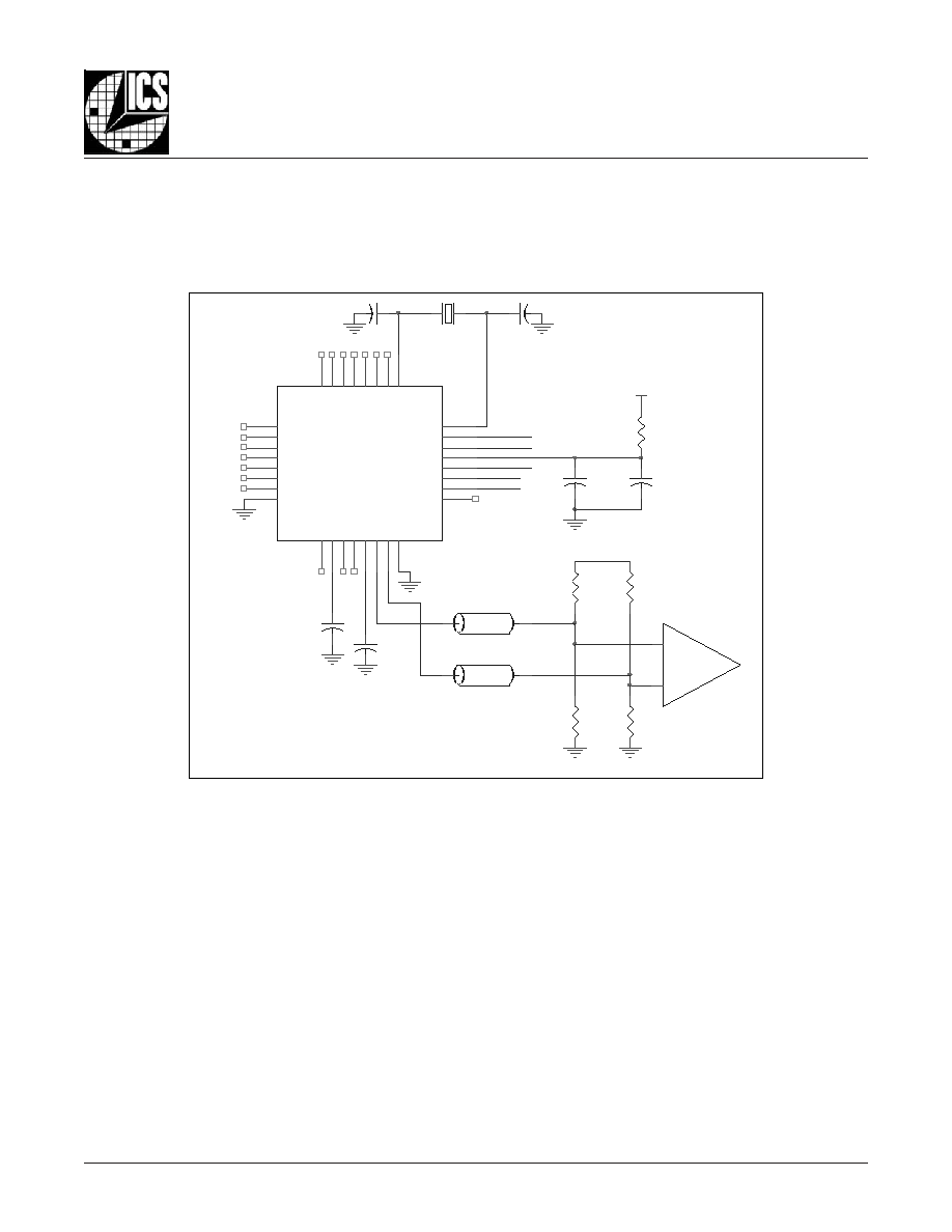
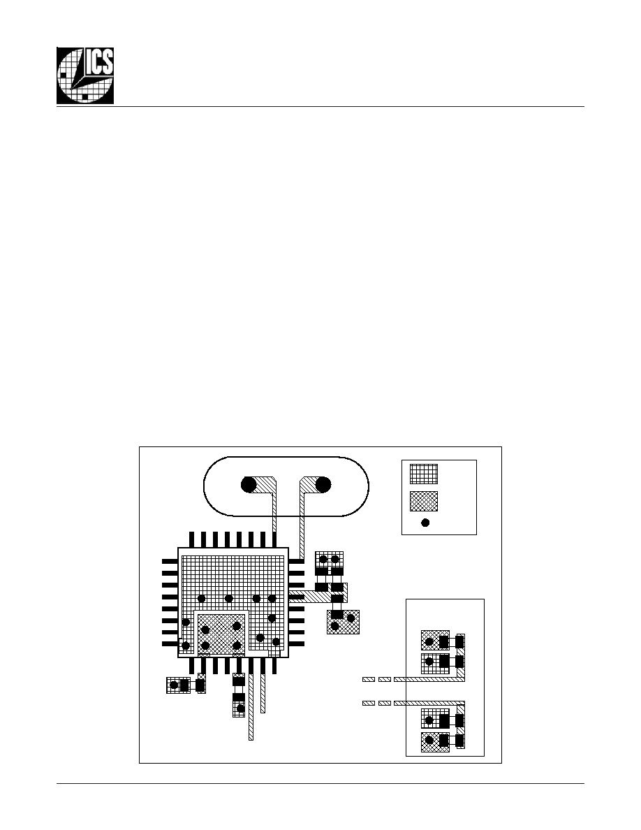
The schematic of the ICS8432-11 layout example used in this
layout guideline is shown in
Figure 4A. The ICS8432-11 recom-
mended PCB board layout for this example is shown in
Figure
4B. This layout example is used as a general guideline. The lay-
L
AYOUT
G
UIDELINE
F
IGURE
4A. S
CHEMATIC
OF
R
ECOMMENDED
L
AYOUT
out in the actual system will depend on the selected component
types, the density of the components, the density of the traces,
and the stacking of the P.C. board.
C16
10u
S_CLOCK
C1
R3
125
C11
0.01u
FO
UT
+
-
IN-
TL2
Zo = 50 Ohm
C15
0.1u
VC
C
IN+
VCCA
FO
UT
N
C2
U1
ICS8432-11
1
2
3
4
5
6
7
8
9
10
11
12
13
14
15
16
17
18
19
20
21
22
23
24
32
31
30
29
28
27
26
25
M5
M6
M7
M8
N0
N1
nc
VEE
TE
S
T
VC
C
FO
UT
/
2
nF
O
U
T
/
2
VC
C
O
FO
UT
nF
O
U
T
VEE
MR
S_CLOCK
S_DATA
S_LOAD
VCCA
XTAL_SEL
T_CLK
X_IN
M4
M3
M2
M1
M0
VC
O_
S
E
L
nP
_
L
OA
D
X_O
U
T
R7
10
S_DATA
VCC
XTAL_SEL
C14
0.1u
REF_IN
VCC=3.3V
VCC
S_LOAD
VC
C
R4
84
TL1
Zo = 50 Ohm
R2
84
R1
125
X1
8432CY-11
www.icst.com/products/hiperclocks.html
REV. E MAY 20, 2005
11
PRELIMINARY
Integrated
Circuit
Systems, Inc.
ICS8432-11
700MH
Z
/350MH
Z
, L
OW
P
HASE
N
OISE
,
C
RYSTAL
-
TO
- 3.3V LVPECL F
REQUENCY
S
YNTHESIZER
F
IGURE
4B. PCB B
OARD
L
AYOUT
FOR
ICS8432-11
TL1, TL2 are 50 Ohm traces and
equal length
C15
C16
VCC
TL
1
R4
VIA
R7
R1
GND
U1
TL1
R3
X1
Close to the input
pins of the
receiver
C14
PIN 1
T
L1N
VCCA
TL1N
R2
C11
The following component footprints are used in this layout
example:
All the resistors and capacitors are size 0603.
P
OWER
AND
G
ROUNDING
Place the decoupling capacitors C14 and C15, as close as pos-
sible to the power pins. If space allows, placement of the
decoupling capacitor on the component side is preferred. This
can reduce unwanted inductance between the decoupling ca-
pacitor and the power pin caused by the via.
Maximize the power and ground pad sizes and number of vias
capacitors. This can reduce the inductance between the power
and ground planes and the component power and ground pins.
The RC filter consisting of R7, C11, and C16 should be placed
as close to the V
CCA
pin as possible.
C
LOCK
T
RACES
AND
T
ERMINATION
Poor signal integrity can degrade the system performance or
cause system failure. In synchronous high-speed digital systems,
the clock signal is less tolerant to poor signal integrity than other
signals. Any ringing on the rising or falling edge or excessive ring
back can cause system failure. The shape of the trace and the
trace delay might be restricted by the available space on the board
and the component location. While routing the traces, the clock
signal traces should be routed first and should be locked prior to
routing other signal traces.
∑ The differential 50
output traces should have same
length.
∑ Avoid sharp angles on the clock trace. Sharp angle
turns cause the characteristic impedance to change on
the transmission lines.
∑ Keep the clock traces on the same layer. Whenever pos-
sible, avoid placing vias on the clock traces. Placement
of vias on the traces can affect the trace characteristic
impedance and hence degrade signal integrity.
∑ To prevent cross talk, avoid routing other signal traces in
parallel with the clock traces. If running parallel traces is
unavoidable, allow a spearation of at least three trace
widths between the differential clock trace and the other
signal trace.
∑ Make sure no other signal traces are routed between the
clock trace pair.
∑ The matching termination resistors should be located as
close to the receiver input pins as possible.
C
RYSTAL
The crystal X1 should be located as close as possible to the pins
24 (XTAL_IN) and 25 (XTAL_OUT). The trace length between the
X1 and U1 should be kept to a minimum to avoid unwanted para-
sitic inductance and capacitance. Other signal traces should not
be routed near the crystal traces.

8432CY-11
www.icst.com/products/hiperclocks.html
REV. E MAY 20, 2005
12
PRELIMINARY
Integrated
Circuit
Systems, Inc.
ICS8432-11
700MH
Z
/350MH
Z
, L
OW
P
HASE
N
OISE
,
C
RYSTAL
-
TO
- 3.3V LVPECL F
REQUENCY
S
YNTHESIZER
P
OWER
C
ONSIDERATIONS
This section provides information on power dissipation and junction temperature for the ICS8432-11.
Equations and example calculations are also provided.
1. Power Dissipation.
The total power dissipation for the ICS8432-11 is the sum of the core power plus the power dissipated in the load(s).
The following is the power dissipation for V
CC
= 3.3V + 5% = 3.465V, which gives worst case results.
NOTE: Please refer to Section 3 for details on calculating power dissipated in the load.
∑
Power (core)
MAX
= V
CC_MAX
* I
EE_MAX
= 3.465V * 110mA = 381.2mW
∑
Power (outputs)
MAX
= 30mW/Loaded Output pair
If all outputs are loaded, the total power is 2 * 30mW = 60mW
Total Power
_MAX
(3.465V, with all outputs switching) = 381.2mW + 60.4mW = 441.2mW
2. Junction Temperature.
Junction temperature, Tj, is the temperature at the junction of the bond wire and bond pad and directly affects the reliability of the
device. The maximum recommended junction temperature for HiPerClockS
TM
devices is 125∞C.
The equation for Tj is as follows: Tj =
JA
* Pd_total + T
A
Tj = Junction Temperature
JA
= Junction-to-Ambient Thermal Resistance
Pd_total = Total Device Power Dissipation (example calculation is in section 1 above)
T
A
= Ambient Temperature
In order to calculate junction temperature, the appropriate junction-to-ambient thermal resistance
JA
must be used. Assuming a
moderate air flow of 200 linear feet per minute and a multi-layer board, the appropriate value is 42.1∞C/W per Table 10 below.
Therefore, Tj for an ambient temperature of 70∞C with all outputs switching is:
70∞C + 0.441W * 42.1∞C/W = 88.6∞C. This is well below the limit of 125∞C.
This calculation is only an example. Tj will obviously vary depending on the number of loaded outputs, supply voltage, air flow,
and the type of board (single layer or multi-layer).
JA
by Velocity (Linear Feet per Minute)
T
ABLE
10. T
HERMAL
R
ESISTANCE
JA
FOR
32-
PIN
LQFP, F
ORCED
C
ONVECTION
0
200
500
Single-Layer PCB, JEDEC Standard Test Boards
67.8∞C/W
55.9∞C/W
50.1∞C/W
Multi-Layer PCB, JEDEC Standard Test Boards
47.9∞C/W
42.1∞C/W
39.4∞C/W
NOTE: Most modern PCB designs use multi-layered boards. The data in the second row pertains to most designs.
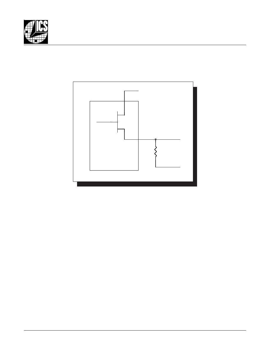
8432CY-11
www.icst.com/products/hiperclocks.html
REV. E MAY 20, 2005
13
PRELIMINARY
Integrated
Circuit
Systems, Inc.
ICS8432-11
700MH
Z
/350MH
Z
, L
OW
P
HASE
N
OISE
,
C
RYSTAL
-
TO
- 3.3V LVPECL F
REQUENCY
S
YNTHESIZER
3. Calculations and Equations.
The purpose of this section is to derive the power dissipated into the load.
LVPECL output driver circuit and termination are shown in
Figure 5.
T
o calculate worst case power dissipation into the load, use the following equations which assume a 50
load, and a termination
voltage of V
CCO
- 2V.
∑
For logic high, V
OUT
= V
OH_MAX
= V
CCO_MAX
≠ 1.0V
(V
CCO_MAX
- V
OH_MAX
) = 1.0V
∑
For logic low, V
OUT
= V
OL_MAX
= V
CCO_MAX
≠ 1.7V
(V
CCO_MAX
- V
OL_MAX
) = 1.7V
Pd_H is power dissipation when the output drives high.
Pd_L is the power dissipation when the output drives low.
Pd_H = [(V
OH_MAX
≠ (V
CCO_MAX
- 2V))/R
L
] * (V
CCO_MAX
- V
OH_MAX
) = [(2V - (V
CCO_MAX
- V
OH_MAX
))/R
L
] * (V
CCO_MAX
- V
OH_MAX
) =
[(2V - 1V)/50
) * 1V = 20.0mW
Pd_L = [(V
OL_MAX
≠ (V
CCO_MAX
- 2V))/R
L
] * (V
CCO_MAX
- V
OL_MAX
) = [(2V - (V
CCO_MAX
- V
OL_MAX
))/R
L
] * (V
CCO_MAX
- V
OL_MAX
) =
[(2V - 1.7V)/50
) * 1.7V = 10.2mW
Total Power Dissipation per output pair = Pd_H + Pd_L = 30.2mW
F
IGURE
5. LVPECL D
RIVER
C
IRCUIT
AND
T
ERMINATION
Q1
V
OUT
V
CCO
R L
50
V
CCO
- 2V

8432CY-11
www.icst.com/products/hiperclocks.html
REV. E MAY 20, 2005
14
PRELIMINARY
Integrated
Circuit
Systems, Inc.
ICS8432-11
700MH
Z
/350MH
Z
, L
OW
P
HASE
N
OISE
,
C
RYSTAL
-
TO
- 3.3V LVPECL F
REQUENCY
S
YNTHESIZER
R
ELIABILITY
I
NFORMATION
T
RANSISTOR
C
OUNT
The transistor count for ICS8432-11 is: 3765
T
ABLE
11.
JA
VS
. A
IR
F
LOW
T
ABLE
FOR
32 L
EAD
LQFP
JA
by Velocity (Linear Feet per Minute)
0
200
500
Single-Layer PCB, JEDEC Standard Test Boards
67.8∞C/W
55.9∞C/W
50.1∞C/W
Multi-Layer PCB, JEDEC Standard Test Boards
47.9∞C/W
42.1∞C/W
39.4∞C/W
NOTE: Most modern PCB designs use multi-layered boards. The data in the second row pertains to most designs.
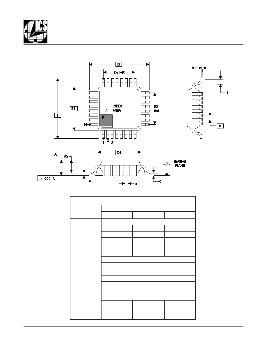
8432CY-11
www.icst.com/products/hiperclocks.html
REV. E MAY 20, 2005
15
PRELIMINARY
Integrated
Circuit
Systems, Inc.
ICS8432-11
700MH
Z
/350MH
Z
, L
OW
P
HASE
N
OISE
,
C
RYSTAL
-
TO
- 3.3V LVPECL F
REQUENCY
S
YNTHESIZER
P
ACKAGE
O
UTLINE
- Y S
UFFIX
FOR
32 L
EAD
LQFP
T
ABLE
12. P
ACKAGE
D
IMENSIONS
Reference Document: JEDEC Publication 95, MS-026
N
O
I
T
A
I
R
A
V
C
E
D
E
J
S
R
E
T
E
M
I
L
L
I
M
N
I
S
N
O
I
S
N
E
M
I
D
L
L
A
L
O
B
M
Y
S
A
B
B
M
U
M
I
N
I
M
L
A
N
I
M
O
N
M
U
M
I
X
A
M
N
2
3
A
-
-
-
-
0
6
.
1
1
A
5
0
.
0
-
-
5
1
.
0
2
A
5
3
.
1
0
4
.
1
5
4
.
1
b
0
3
.
0
7
3
.
0
5
4
.
0
c
9
0
.
0
-
-
0
2
.
0
D
C
I
S
A
B
0
0
.
9
1
D
C
I
S
A
B
0
0
.
7
2
D
.
f
e
R
0
6
.
5
E
C
I
S
A
B
0
0
.
9
1
E
C
I
S
A
B
0
0
.
7
2
E
.
f
e
R
0
6
.
5
e
C
I
S
A
B
0
8
.
0
L
5
4
.
0
0
6
.
0
5
7
.
0
0
∞
-
-
7
∞
c
c
c
-
-
-
-
0
1
.
0
8432CY-11
www.icst.com/products/hiperclocks.html
REV. E MAY 20, 2005
16
PRELIMINARY
Integrated
Circuit
Systems, Inc.
ICS8432-11
700MH
Z
/350MH
Z
, L
OW
P
HASE
N
OISE
,
C
RYSTAL
-
TO
- 3.3V LVPECL F
REQUENCY
S
YNTHESIZER
T
ABLE
13. O
RDERING
I
NFORMATION
While the information presented herein has been checked for both accuracy and reliability, Integrated Circuit Systems, Incorporated (ICS) assumes no responsibility for either its use
or for infringement of any patents or other rights of third parties, which would result from its use. No other circuits, patents, or licenses are implied. This product is intended for use
in normal commercial applications. Any other applications such as those requiring extended temperature range, high reliability, or other extraordinary environmental requirements are
not recommended without additional processing by ICS. ICS reserves the right to change any circuitry or specifications without notice. ICS does not authorize or warrant any ICS
product for use in life support devices or critical medical instruments.
r
e
b
m
u
N
r
e
d
r
O
/
t
r
a
P
g
n
i
k
r
a
M
e
g
a
k
c
a
P
g
n
i
g
a
k
c
a
P
g
n
i
p
p
i
h
S
e
r
u
t
a
r
e
p
m
e
T
1
1
-
Y
C
2
3
4
8
S
C
I
1
1
-
Y
C
2
3
4
8
S
C
I
P
F
Q
L
d
a
e
L
2
3
y
a
r
t
C
∞
0
7
o
t
C
∞
0
T
1
1
-
Y
C
0
3
4
8
S
C
I
1
1
-
Y
C
2
3
4
8
S
C
I
P
F
Q
L
d
a
e
L
2
3
l
e
e
r
&
e
p
a
t
0
0
0
1
C
∞
0
7
o
t
C
∞
0
The aforementioned trademark, HiPerClockSTM is a trademark of Integrated Circuit Systems, Inc. or its subsidiaries in the United States and/or other countries.