855011AM
www.icst.com/products/hiperclocks.html
REV. A AUGUST 18, 2004
1
Integrated
Circuit
Systems, Inc.
ICS855011
L
OW
S
KEW
, 1-
TO
-2
D
IFFERENTIAL
-
TO
-2.5V/3.3V CML F
ANOUT
B
UFFER
PRELIMINARY
G
ENERAL
D
ESCRIPTION
The ICS85 5011 is a low skew, high perfor-
mance 1 - t o - 2 Differential-to-2.5V/3.3V CML
F a n o u t B u f f e r a n d a m e m b e r o f t h e
HiPerClockS TM
family of High Perfor mance
Clock Solutions from ICS. The ICS855011
is characterized to operate from either a 2.5V or a 3.3V
power supply. Guaranteed output and par t-to-par t skew
characteristics make the ICS855011 ideal for those
clock distribution applications demanding well defined
perfor mance and repeatability.
F
EATURES
· 2 differential 2.5V/3.3V CML outputs
· 1 differential PCLK, nPCLK input pair
· PCLK, nPCLK pair can accept the following
differential input levels: LVPECL, LVDS, CML, SSTL
· Output frequency: >3GHz
· Translates any single ended input signal to 3.3V
LVPECL levels with resistor bias on nPCLK input
· Output skew: 5ps (typical)
· Part-to-part skew: TBD
· Propagation delay: 242ps (typical)
· Operating voltage supply range:
V
CC
= 2.375V to 3.8V, V
EE
= 0V
· -40°C to 85°C ambient operating temperature
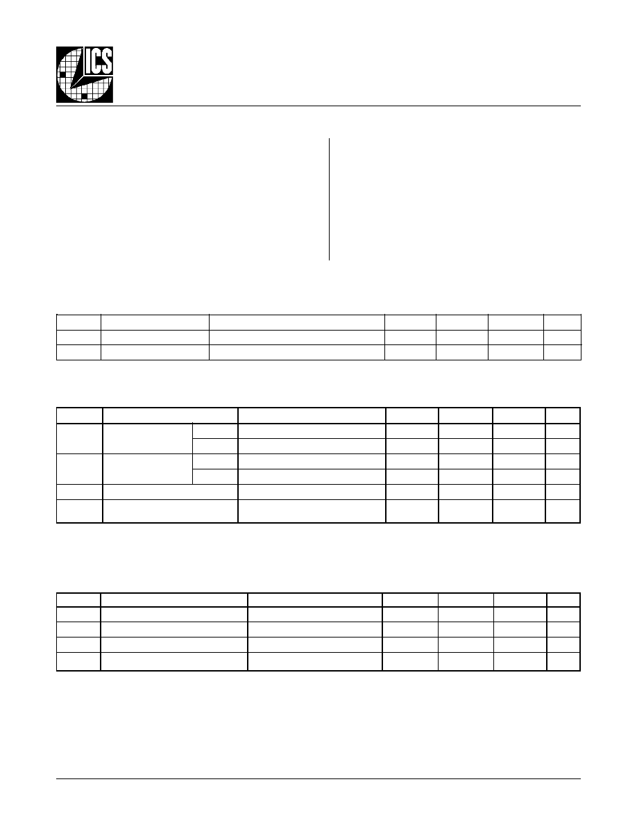
B
LOCK
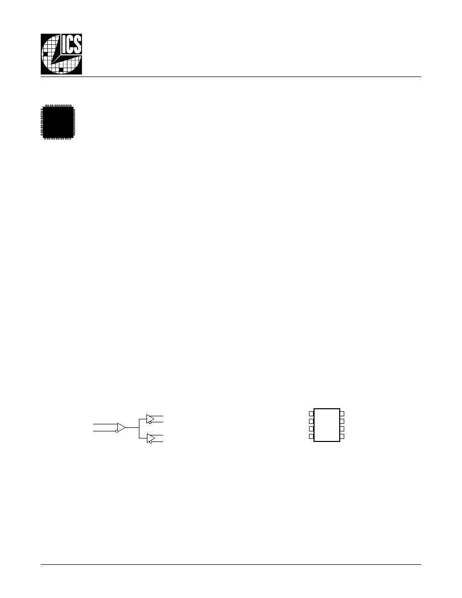
D
IAGRAM
P
IN
A
SSIGNMENT
ICS855011
8-Lead SOIC
3.90mm x 4.90mm x 1.37mm package body
M Package
Top View
Q0
nQ0
Q1
nQ1
1
2
3
4
HiPerClockSTM
ICS
Vcc
PCLK
nPCLK
V
EE
8
7
6
5
Q0
nQ0
Q1
nQ1
PCLK
nPCLK
The Preliminary Information presented herein represents a product in prototyping or pre-production. The noted characteristics are based on initial
product characterization. Integrated Circuit Systems, Incorporated (ICS) reserves the right to change any circuitry or specifications without notice.
855011AM
www.icst.com/products/hiperclocks.html
REV. A AUGUST 18, 2004
3
Integrated
Circuit
Systems, Inc.
ICS855011
L
OW
S
KEW
, 1-
TO
-2
D
IFFERENTIAL
-
TO
-2.5V/3.3V CML F
ANOUT
B
UFFER
PRELIMINARY
T
ABLE
3A. P
OWER
S
UPPLY
DC C
HARACTERISTICS
,
V
CC
= 2.375V
TO
3.8V; V
EE
= 0V
l
o
b
m
y
S
r
e
t
e
m
a
r
a
P
s
n
o
i
t
i
d
n
o
C
t
s
e
T
m
u
m
i
n
i
M
l
a
c
i
p
y
T
m
u
m
i
x
a
M
s
t
i
n
U
V
C
C
e
g
a
t
l
o
V
y
l
p
p
u
S
e
v
i
t
i
s
o
P
5
7
3
.
2
3
.
3
8
.
3
V
I
E
E
t
n
e
r
r
u
C
y
l
p
p
u
S
r
e
w
o
P
0
5
A
m
A
BSOLUTE
M
AXIMUM
R
ATINGS
T
ABLE
3B. LVPECL DC C
HARACTERISTICS
,
V
CC
= 2.375V
TO
3.8V; V
EE
= 0V
NOTE: Stresses beyond those listed under Absolute
Maximum Ratings may cause permanent damage
to the device. These ratings are stress specifi-
cations only. Functional operation of product at
these conditions or any conditions beyond those
listed in the
DC Characteristics or AC Character-
istics is not implied. Exposure to absolute maxi-
mum rating conditions for extended periods may
affect product reliability.
Supply Voltage, V
CC
4.6V (CML mode, V
EE
= 0)
Inputs, V
I
-0.5V to V
CC
+ 0.5 V
Outputs, I
O
Continuous Current
20mA
Surge Current
40mA
Operating Temperature Range, TA -40°C to +85°C
Storage Temperature, T
STG
-65°C to 150°C
Package Thermal Impedance,
JA
112.7°C/W (0 lfpm)
(Junction-to-Ambient)
T
ABLE
3C. CML DC C
HARACTERISTICS
,
V
CC
= 2.375V
TO
3.8V; V
EE
= 0V
l
o
b
m
y
S
r
e
t
e
m
a
r
a
P
s
n
o
i
t
i
d
n
o
C
m
u
m
i
n
i
M
l
a
c
i
p
y
T
m
u
m
i
x
a
M
s
t
i
n
U
V
H
O
1
E
T
O
N
;
e
g
a
t
l
o
V
h
g
i
H
t
u
p
t
u
O
V
C
C
0
2
0
.
0
-
V
C
C
0
1
0
.
0
-
V
C
C
V
V
T
U
O
g
n
i
w
S
e
g
a
t
l
o
V
t
u
p
t
u
O
5
2
3
0
0
4
V
m
V
T
U
O
_
F
F
I
D
g
n
i
w
S
e
g
a
t
l
o
V
t
u
p
t
u
O
l
a
i
t
n
e
r
e
f
f
i
D
0
5
6
0
0
8
V
m
R
T
U
O
e
c
n
a
d
e
p
m
I
e
c
r
u
o
S
t
u
p
t
u
O
0
4
0
5
0
6
0
0
1
h
t
i
w
d
e
t
a
n
i
m
r
e
t
s
t
u
p
t
u
O
:
1
E
T
O
N
.
r
i
a
p
t
u
p
t
u
o
l
a
i
t
n
e
r
e
f
f
i
d
s
s
o
r
c
a
l
o
b
m
y
S
r
e
t
e
m
a
r
a
P
s
n
o
i
t
i
d
n
o
C
t
s
e
T
m
u
m
i
n
i
M
l
a
c
i
p
y
T
m
u
m
i
x
a
M
s
t
i
n
U
I
H
I
t
n
e
r
r
u
C
h
g
i
H
t
u
p
n
I
K
L
C
P
V
C
C
V
=
N
I
V
8
.
3
=
0
5
1
A
µ
K
L
C
P
n
V
C
C
V
=
N
I
V
8
.
3
=
5
A
µ
I
L
I
t
n
e
r
r
u
C
w
o
L
t
u
p
n
I
K
L
C
P
V
C
C
V
,
V
8
.
3
=
N
I
V
0
=
5
-
A
µ
K
L
C
P
n
V
C
C
V
,
V
8
.
3
=
N
I
V
0
=
0
5
1
-
A
µ
V
P
P
e
g
a
t
l
o
V
t
u
p
n
I
k
a
e
P
-
o
t
-
k
a
e
P
3
.
0
1
V
V
R
M
C
;
e
g
a
t
l
o
V
t
u
p
n
I
e
d
o
M
n
o
m
m
o
C
2
,
1
E
T
O
N
V
E
E
5
.
1
+
V
C
C
V
V
s
a
d
e
n
i
f
e
d
s
i
e
g
a
t
l
o
v
e
d
o
m
n
o
m
m
o
C
:
1
E
T
O
N
H
I
.
V
s
i
K
L
C
P
n
d
n
a
K
L
C
P
r
o
f
e
g
a
t
l
o
v
t
u
p
n
i
m
u
m
i
x
a
m
e
h
t
,
s
n
o
i
t
a
c
il
p
p
a
d
e
d
n
e
e
l
g
n
i
s
r
o
F
:
2
E
T
O
N
C
C
.
V
3
.
0
+