858011AK
www.icst.com/products/hiperclocks.html
REV. A JULY 12, 2004
1
Integrated
Circuit
Systems, Inc.
ICS858011
L
OW
S
KEW
, 1-
TO
-2
D
IFFERENTIAL
-
TO
-CML F
ANOUT
B
UFFER
PRELIMINARY
G
ENERAL
D
ESCRIPTION
The ICS858011 is a high speed 1-to-2 Differential-
to-CML Fanout Buffer and is a member of the
HiPerClockS
TM
family of high performance clock
solutions from ICS. The ICS858011 is optimized
for high speed and very low output skew, making
it suitable for use in demanding applications such as SONET,
1 Gigabit and 10 Gigabit Ethernet, and Fibre Channel. The
internally terminated differential input and V
REF
_
AC
pin allow
other differential signal families such as LVDS, LVHSTL and
CML to be easily interfaced to the input with minimal use of
external components. The ICS858011 is packaged in a small
3mm x 3mm 16-pin VFQFN package which makes it ideal for
use in space-constrained applications.
F
EATURES
· 2 differential CML outputs
· 1 differential LVPECL clock input
· IN, nIN pair can accept the following differential input levels:
LVPECL, LVDS, CML, SSTL
· Output frequency: > 2.5GHz (typical)
· Output skew: TBD
· Part-to-part skew: TBD
· Additive phase jitter, RMS: <100fs (design target)
· Propagation delay: 388ps (typical)
· Operating voltage supply range:
V
CC
= 2.375V to 3.63V, V
EE
= 0V
· -40°C to 85°C ambient operating temperature
· Pin compatible with SY58011U
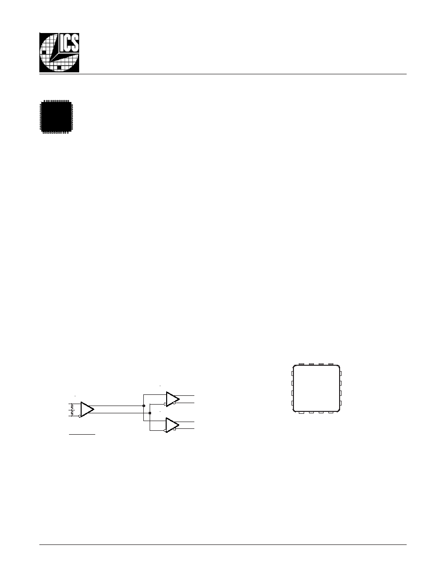
B
LOCK
D
IAGRAM
P
IN
A
SSIGNMENT
HiPerClockSTM
ICS
IN
V
T
nIN
Q0
nQ0
Q1
nQ1
V
REF_AC
ICS858011
16-Lead VFQFN
3mm x 3mm x 0.95 package body
K Package
Top View
IN
V
T
V
REF
_
AC
nIN
Q0
nQ0
nQ1
Q1
V
CC
V
EE
V
EE
V
CC
V
CC
V
EE
V
EE
V
CC
1
2
3
4
12
11
10
9
5 6 7 8
16 15 14 13
The Preliminary Information presented herein represents a product in prototyping or pre-production. The noted characteristics are based on initial
product characterization. Integrated Circuit Systems, Incorporated (ICS) reserves the right to change any circuitry or specifications without notice.

858011AK
www.icst.com/products/hiperclocks.html
REV. A JULY 12, 2004
2
Integrated
Circuit
Systems, Inc.
ICS858011
L
OW
S
KEW
, 1-
TO
-2
D
IFFERENTIAL
-
TO
-CML F
ANOUT
B
UFFER
PRELIMINARY
T
ABLE
1. P
IN
D
ESCRIPTIONS
r
e
b
m
u
N
e
m
a
N
e
p
y
T
n
o
i
t
p
i
r
c
s
e
D
1
N
I
t
u
p
n
I
.
t
u
p
n
i
k
c
o
l
c
l
a
i
t
n
e
r
e
f
f
i
d
L
C
E
P
V
L
g
n
i
t
r
e
v
n
i
-
n
o
N
2
V
T
t
u
p
n
I
.
t
u
p
n
i
n
o
i
t
a
n
i
m
r
e
T
3
V
C
A
_
F
E
R
t
u
p
t
u
O
.
s
n
o
i
t
a
c
il
p
p
a
d
e
l
p
u
o
c
-
C
A
r
o
f
e
g
a
t
l
o
v
e
c
n
e
r
e
f
e
R
V
C
A
_
F
E
R
V
o
t
=
C
C
.
V
8
3
.
1
-
4
N
I
n
t
u
p
n
I
.
t
u
p
n
i
k
c
o
l
c
L
C
E
P
V
L
l
a
i
t
n
e
r
e
f
f
i
d
g
n
i
t
r
e
v
n
I
6
1
,
3
1
,
8
,
5
V
C
C
r
e
w
o
P
.
s
n
i
p
y
l
p
p
u
s
e
v
i
t
i
s
o
P
5
1
,
4
1
,
7
,
6
V
E
E
r
e
w
o
P
.
n
i
p
y
l
p
p
u
s
e
v
i
t
a
g
e
N
0
1
,
9
1
Q
n
,
1
Q
t
u
p
t
u
O
.
s
l
e
v
e
l
e
c
a
f
r
e
t
n
i
L
M
C
.
r
i
a
p
t
u
p
t
u
o
l
a
i
t
n
e
r
e
f
f
i
D
2
1
,
1
1
0
Q
,
0
Q
n
t
u
p
t
u
O
.
s
l
e
v
e
l
e
c
a
f
r
e
t
n
i
L
M
C
.
r
i
a
p
t
u
p
t
u
o
l
a
i
t
n
e
r
e
f
f
i
D
858011AK
www.icst.com/products/hiperclocks.html
REV. A JULY 12, 2004
3
Integrated
Circuit
Systems, Inc.
ICS858011
L
OW
S
KEW
, 1-
TO
-2
D
IFFERENTIAL
-
TO
-CML F
ANOUT
B
UFFER
PRELIMINARY
T
ABLE
2A. P
OWER
S
UPPLY
DC C
HARACTERISTICS
,
V
CC
= 2.375V
TO
3.63V; V
EE
= 0V
l
o
b
m
y
S
r
e
t
e
m
a
r
a
P
s
n
o
i
t
i
d
n
o
C
t
s
e
T
m
u
m
i
n
i
M
l
a
c
i
p
y
T
m
u
m
i
x
a
M
s
t
i
n
U
V
C
C
e
g
a
t
l
o
V
y
l
p
p
u
S
e
v
i
t
i
s
o
P
5
7
3
.
2
3
.
3
3
6
.
3
V
I
E
E
t
n
e
r
r
u
C
y
l
p
p
u
S
r
e
w
o
P
D
B
T
A
m
A
BSOLUTE
M
AXIMUM
R
ATINGS
NOTE: Stresses beyond those listed under Absolute
Maximum Ratings may cause permanent damage
to the device. These ratings are stress specifi-
cations only. Functional operation of product at
these conditions or any conditions beyond those
listed in the
DC Characteristics or AC Character-
istics is not implied. Exposure to absolute maxi-
mum rating conditions for extended periods may
affect product reliability.
Supply Voltage, V
CC
4.6V (CML mode, V
EE
= 0)
Inputs, V
I
-0.5V to V
CC
+ 0.5 V
Outputs, I
O
Continuous Current
20mA
Surge Current
40mA
Input Current, IN, nIN
±50mA
V
T
Current, I
VT
±100mA
Input Sink/Source, I
REF_AC
± 0.5mA
Operating Temperature Range, TA -40°C to +85°C
Storage Temperature, T
STG
-65°C to 150°C
Package Thermal Impedance,
JA
51.5°C/W (0 lfpm)
(Junction-to-Ambient)
T
ABLE
2B. DC C
HARACTERISTICS
,
V
CC
= 2.375V
TO
3.63V; V
EE
= 0V
l
o
b
m
y
S
r
e
t
e
m
a
r
a
P
s
n
o
i
t
i
d
n
o
C
t
s
e
T
m
u
m
i
n
i
M
l
a
c
i
p
y
T
m
u
m
i
x
a
M
s
t
i
n
U
R
N
I
e
c
n
a
t
s
i
s
e
R
t
u
p
n
I
l
a
i
t
n
e
r
e
f
f
i
D
)
N
I
n
,
N
I
(
0
0
1
V
H
I
e
g
a
t
l
o
V
h
g
i
H
t
u
p
n
I
)
N
I
n
,
N
I
(
2
.
1
V
C
C
V
V
L
I
e
g
a
t
l
o
V
w
o
L
t
u
p
n
I
)
N
I
n
,
N
I
(
0
V
H
I
5
1
.
0
-
V
V
N
I
1
E
T
O
N
;
g
n
i
w
S
e
g
a
t
l
o
V
t
u
p
n
I
5
1
.
0
8
.
2
V
V
N
I
_
F
F
I
D
g
n
i
w
S
e
g
a
t
l
o
V
t
u
p
n
I
l
a
i
t
n
e
r
e
f
f
i
D
3
.
0
V
I
N
I
t
n
e
r
r
u
C
t
u
p
n
I
)
N
I
n
,
N
I
(
5
3
A
m
m
a
r
g
a
i
D
g
n
i
w
S
e
g
a
t
l
o
V
t
u
p
n
I
,
n
o
i
t
a
m
r
o
f
n
I
t
n
e
m
e
r
u
s
a
e
M
r
e
t
e
m
a
r
a
P
o
t
r
e
f
e
R
:
1
E
T
O
N
T
ABLE
2C. CML DC C
HARACTERISTICS
,
V
CC
= 2.375V
TO
3.63V; V
EE
= 0V
l
o
b
m
y
S
r
e
t
e
m
a
r
a
P
s
n
o
i
t
i
d
n
o
C
m
u
m
i
n
i
M
l
a
c
i
p
y
T
m
u
m
i
x
a
M
s
t
i
n
U
V
H
O
1
E
T
O
N
;
e
g
a
t
l
o
V
h
g
i
H
t
u
p
t
u
O
V
C
C
0
2
0
.
0
-
V
C
C
0
1
0
.
0
-
V
C
C
V
V
T
U
O
g
n
i
w
S
e
g
a
t
l
o
V
t
u
p
t
u
O
5
2
3
0
0
4
V
m
V
T
U
O
_
F
F
I
D
g
n
i
w
S
e
g
a
t
l
o
V
t
u
p
t
u
O
l
a
i
t
n
e
r
e
f
f
i
D
0
5
6
0
0
8
V
m
R
T
U
O
e
c
n
a
d
e
p
m
I
e
c
r
u
o
S
t
u
p
t
u
O
0
4
0
5
0
6
0
0
1
h
t
i
w
d
e
t
a
n
i
m
r
e
t
s
t
u
p
t
u
O
:
1
E
T
O
N
.
r
i
a
p
t
u
p
t
u
o
l
a
i
t
n
e
r
e
f
f
i
d
s
s
o
r
c
a
858011AK
www.icst.com/products/hiperclocks.html
REV. A JULY 12, 2004
4
Integrated
Circuit
Systems, Inc.
ICS858011
L
OW
S
KEW
, 1-
TO
-2
D
IFFERENTIAL
-
TO
-CML F
ANOUT
B
UFFER
PRELIMINARY
T
ABLE
3. AC C
HARACTERISTICS
,
V
CC
= 0V; V
EE
= -3.63V
TO
-2.375V
OR
V
CC
= 2.375
TO
3.63V; V
EE
= 0V
l
o
b
m
y
S
r
e
t
e
m
a
r
a
P
n
o
i
t
i
d
n
o
C
m
u
m
i
n
i
M
l
a
c
i
p
y
T
m
u
m
i
x
a
M
s
t
i
n
U
f
X
A
M
y
c
n
e
u
q
e
r
F
t
u
p
t
u
O
5
.
2
>
z
H
G
t
D
P
;
)
l
a
i
t
n
e
r
e
f
f
i
D
(
;
y
a
l
e
D
n
o
i
t
a
g
a
p
o
r
P
1
E
T
O
N
8
8
3
s
p
t
)
o
(
k
s
4
,
2
E
T
O
N
;
w
e
k
S
t
u
p
t
u
O
D
B
T
s
p
t
)
p
p
(
k
s
4
,
3
E
T
O
N
;
w
e
k
S
t
r
a
P
-
o
t
-
t
r
a
P
D
B
T
s
p
t t
ij
;
S
M
R
,
r
e
t
t
i
J
e
s
a
h
P
e
v
i
t
i
d
d
A
r
e
f
f
u
B
n
o
i
t
c
e
s
r
e
t
t
i
J
e
s
a
h
P
e
v
i
t
i
d
d
A
o
t
r
e
f
e
r
0
0
1
<
s
f
t
R
/t
F
e
m
i
T
ll
a
F
/
e
s
i
R
t
u
p
t
u
O
%
0
8
o
t
%
0
2
0
2
1
s
p
t
a
d
e
z
i
r
e
t
c
a
r
a
h
c
s
r
e
t
e
m
a
r
a
p
ll
A
.
d
e
t
o
n
e
s
i
w
r
e
h
t
o
s
s
e
l
n
u
z
H
G
1
R
L
0
0
1
=
.
r
i
a
p
t
u
p
t
u
o
h
c
a
e
r
e
t
f
a
.
t
n
i
o
p
g
n
i
s
s
o
r
c
t
u
p
t
u
o
l
a
i
t
n
e
r
e
f
f
i
d
e
h
t
o
t
t
n
i
o
p
g
n
i
s
s
o
r
c
t
u
p
n
i
l
a
i
t
n
e
r
e
f
f
i
d
e
h
t
m
o
r
f
d
e
r
u
s
a
e
M
:
1
E
T
O
N
.
s
n
o
i
t
i
d
n
o
c
d
a
o
l
l
a
u
q
e
h
t
i
w
d
n
a
e
g
a
t
l
o
v
y
l
p
p
u
s
e
m
a
s
e
h
t
t
a
s
t
u
p
t
u
o
n
e
e
w
t
e
b
w
e
k
s
s
a
d
e
n
i
f
e
D
:
2
E
T
O
N
.
s
t
n
i
o
p
s
s
o
r
c
l
a
i
t
n
e
r
e
f
f
i
d
t
u
p
t
u
o
e
h
t
t
a
d
e
r
u
s
a
e
M
s
e
g
a
t
l
o
v
y
l
p
p
u
s
e
m
a
s
e
h
t
t
a
g
n
i
t
a
r
e
p
o
s
e
c
i
v
e
d
t
n
e
r
e
f
f
i
d
n
o
s
t
u
p
t
u
o
n
e
e
w
t
e
b
w
e
k
s
s
a
d
e
n
i
f
e
D
:
3
E
T
O
N
d
e
r
u
s
a
e
m
e
r
a
s
t
u
p
t
u
o
e
h
t
,
e
c
i
v
e
d
h
c
a
e
n
o
s
t
u
p
n
i
f
o
e
p
y
t
e
m
a
s
e
h
t
g
n
i
s
U
.
s
n
o
i
t
i
d
n
o
c
d
a
o
l
l
a
u
q
e
h
t
i
w
d
n
a
.
s
t
n
i
o
p
s
s
o
r
c
l
a
i
t
n
e
r
e
f
f
i
d
e
h
t
t
a
.
5
6
d
r
a
d
n
a
t
S
C
E
D
E
J
h
t
i
w
e
c
n
a
d
r
o
c
c
a
n
i
d
e
n
i
f
e
d
s
i
r
e
t
e
m
a
r
a
p
s
i
h
T
:
4
E
T
O
N
858011AK
www.icst.com/products/hiperclocks.html
REV. A JULY 12, 2004
5
Integrated
Circuit
Systems, Inc.
ICS858011
L
OW
S
KEW
, 1-
TO
-2
D
IFFERENTIAL
-
TO
-CML F
ANOUT
B
UFFER
PRELIMINARY
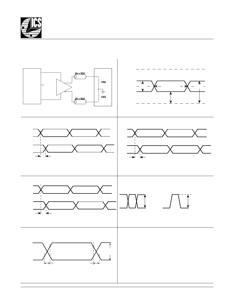
P
ARAMETER
M
EASUREMENT
I
NFORMATION
O
UTPUT
L
OAD
AC T
EST
C
IRCUIT
D
IFFERENTIAL
I
NPUT
L
EVEL
O
UTPUT
S
KEW
P
ART
-
TO
-P
ART
S
KEW
O
UTPUT
R
ISE
/F
ALL
T
IME
P
ROPAGATION
D
ELAY
S
INGLE
E
NDED
& D
IFFERENTIAL
I
NPUT
V
OLTAGE
S
WING
V
EE
nIN
V
CC
IN
tsk(pp)
tsk(o)
nQx
Qx
nQy
Qy
PART 1
PART 2
nQx
Qx
nQy
Qy
Clock
Outputs
20%
80%
80%
20%
t
R
t
F
V
SW I N G
t
PD
nIN
Q0, Q1
nQ0, nQ1
IN
V
IN
, V
OUT
400mV
(typical)
V
DIFF_IN
, V
DIFF_OUT
800mV
(typical)
V
IH
Cross Points
V
IN
V
IL
SCOPE
nQx
Qx
Power
Supply
V
EE
V
CC
Float
GND
GND
3.3V ± 5%
or
2.5V ± 5%
CML with Internal Pullup
+
-
V
IN
V
DIF_IN