Document Outline
- General Description
- Features
- Block Diagram
- Pin Assignment
- Pin Description
- Pin Characteristics
- Control Input Function Table
- PLL Bypass Function Table
- Absolute Maximum Ratings
- Power Supply DC Characteristics
- LVCMOS DC Characteristics
- Differential DC Characteristics
- LVHSTL DC Characteristics
- Input Frequency Characteristics
- AC Characteristics
- Parameter Measurement Information
- Output Load Test Circuit Diagram
- Differential Input Level Diagram
- Output Skew Diagram
- Cycle-to-Cycle Jitter Diagram
- Phase Jitter & Static Phase Offset Diagram
- Output Rise & Fall Time Diagram
- Propagation Delay Diagram
- odc & tPeriod Diagram
- Application Information
- Power Supply Filtering Techniques
- Power Supply Filtering Diagram
- Wiring the Differential Input to Accept Single Ended Levels
- Single Ended Signal Driving Differential Input Diagram
- Layout Guideline
- LVHSTL 0-Delay Buffer Schematic Example
- Power & Grounding
- Clock Traces & Termination
- PCB Board Layout
- Power Considerations
- Power Dissipation
- Junction Temperature
- Thermal Resistance
- Calculations & Equations
- LVHSTL Driver Circuit & Termination
- Reliability Information
- Transistor Count
- Package Outline
- Package Dimensions
- Ordering Information
- Revision History
8624BYI
www.icst.com/products/hiperclocks.html
REV. A OCTOBER 8, 2002
1
Integrated
Circuit
Systems, Inc.
ICS8624I
L
OW
S
KEW
, 1-
TO
-5
D
IFFERENTIAL
-
TO
-LVHSTL Z
ERO
D
ELAY
B
UFFER
G
ENERAL
D
ESCRIPTION
The ICS8624I is a high performance, 1-to-5
Differential-to-LVHSTL zero delay buffer and
a member of the HiPerClockSTM family of High
Performance Clock Solutions from ICS. The
ICS8624I has two selectable clock input pairs.
The CLK0, nCLK0 and CLK1, nCLK1 pair can accept most
standard differential input levels. The VCO operates at a fre-
quency range of 250MHz to 630MHz. Utilizing one of the
outputs as feedback to the PLL, output frequencies up to
630MHz can be regenerated with zero delay with respect to
the input. Dual reference clock inputs support redundant clock
or multiple reference applications.
B
LOCK
D
IAGRAM
P
IN
A
SSIGNMENT
F
EATURES
�
Fully integrated PLL
�
5 differential LVHSTL compatible outputs
�
Selectable differential CLKx, nCLKx input pairs
�
CLKx, nCLKx pairs can accept the following differential
input levels: LVDS, LVPECL, LVHSTL, SSTL, HCSL
�
Output frequency range: 31.25MHz to 630MHz
�
Input frequency range: 31.25MHz to 630MHz
�
VCO range: 250MHz to 630MHz
�
External feedback for "zero delay" clock regeneration
�
Cycle-to-cycle jitter: 35ps (maximum)
�
Output skew: 50ps (maximum)
�
Static phase offset: 30ps �125ps
�
3.3V core, 1.8V output operating supply
�
-40�C to 85�C ambient operating temperature
32 31 30 29 28 27 26 25
9 10 11 12 13 14 15 16
1
2
3
4
5
6
7
8
24
23
22
21
20
19
18
17
V
DDO
Q3
nQ3
Q2
nQ2
Q1
nQ1
V
DDO
SEL0
SEL1
CLK0
nCLK0
CLK1
nCLK1
CLK_SEL
MR
V
DDO
Q0
nQ0
GND
GND
FB_IN
nFB_IN
V
DD
V
DDO
nQ4
Q4
GND
GND
V
DDA
PLL_SEL
V
DD
32-Lead LQFP
7mm x 7mm x 1.4mm body package
Y Package
Top View
ICS8624I
HiPerClockSTM
,&6
PLL_SEL
CLK0
nCLK0
CLK1
nCLK1
CLK_SEL
FB_IN
nFB_IN
SEL0
SEL1
MR
Q0
nQ0
Q1
nQ1
Q2
nQ2
Q3
nQ3
Q4
nQ4
0
1
PLL
0
1
�4, �8

Integrated
Circuit
Systems, Inc.
ICS8624I
L
OW
S
KEW
, 1-
TO
-5
D
IFFERENTIAL
-
TO
-LVHSTL Z
ERO
D
ELAY
B
UFFER
8624BYI
www.icst.com/products/hiperclocks.html
REV. A OCTOBER 8, 2002
2
T
ABLE
1. P
IN
D
ESCRIPTIONS
r
e
b
m
u
N
e
m
a
N
e
p
y
T
n
o
i
t
p
i
r
c
s
e
D
1
0
L
E
S
t
u
p
n
I
n
w
o
d
ll
u
P
.
3
e
l
b
a
T
n
i
d
e
t
o
n
e
g
n
a
r
y
c
n
e
u
q
e
r
f
t
u
p
t
u
o
d
n
a
t
u
p
n
i
e
h
t
s
e
n
i
m
r
e
t
e
D
.
s
l
e
v
e
l
e
c
a
f
r
e
t
n
i
L
T
T
V
L
/
S
O
M
C
V
L
2
1
L
E
S
t
u
p
n
I
n
w
o
d
ll
u
P
.
3
e
l
b
a
T
n
i
d
e
t
o
n
e
g
n
a
r
y
c
n
e
u
q
e
r
f
t
u
p
t
u
o
d
n
a
t
u
p
n
i
e
h
t
s
e
n
i
m
r
e
t
e
D
.
s
l
e
v
e
l
e
c
a
f
r
e
t
n
i
L
T
T
V
L
/
S
O
M
C
V
L
3
0
K
L
C
t
u
p
n
I
n
w
o
d
ll
u
P
.
t
u
p
n
i
k
c
o
l
c
l
a
i
t
n
e
r
e
f
f
i
d
g
n
i
t
r
e
v
n
i
-
n
o
N
4
0
K
L
C
n
t
u
p
n
I
p
u
ll
u
P
.
t
u
p
n
i
k
c
o
l
c
l
a
i
t
n
e
r
e
f
f
i
d
g
n
i
t
r
e
v
n
I
5
1
K
L
C
t
u
p
n
I
n
w
o
d
ll
u
P
.
t
u
p
n
i
k
c
o
l
c
l
a
i
t
n
e
r
e
f
f
i
d
g
n
i
t
r
e
v
n
i
-
n
o
N
6
1
K
L
C
n
t
u
p
n
I
p
u
ll
u
P
.
t
u
p
n
i
k
c
o
l
c
l
a
i
t
n
e
r
e
f
f
i
d
g
n
i
t
r
e
v
n
I
7
L
E
S
_
K
L
C
t
u
p
n
I
n
w
o
d
ll
u
P
s
t
c
e
l
e
s
,
H
G
I
H
n
e
h
W
.
0
K
L
C
n
,
0
K
L
C
s
t
c
e
l
e
s
,
W
O
L
n
e
h
W
.
t
u
p
n
i
t
c
e
l
e
s
k
c
o
l
C
.
s
l
e
v
e
l
e
c
a
f
r
e
t
n
i
L
T
T
V
L
/
S
O
M
C
V
L
.
s
t
u
p
n
i
1
K
L
C
n
,
1
K
L
C
8
R
M
t
u
p
n
I
n
w
o
d
ll
u
P
s
r
e
d
i
v
i
d
l
a
n
r
e
t
n
i
e
h
t
,
H
G
I
H
s
i
c
i
g
o
l
n
e
h
W
.
t
e
s
e
R
r
e
t
s
a
M
H
G
I
H
e
v
i
t
c
A
.
d
e
l
b
a
s
i
d
s
i
t
e
s
e
R
r
e
t
s
a
M
e
h
t
,
W
O
L
n
e
h
W
.
t
e
s
e
r
e
r
a
.
s
l
e
v
e
l
e
c
a
f
r
e
t
n
i
L
T
T
V
L
/
S
O
M
C
V
L
2
3
,
9
V
D
D
r
e
w
o
P
.
s
n
i
p
y
l
p
p
u
s
e
r
o
C
0
1
N
I
_
B
F
n
t
u
p
n
I
p
u
ll
u
P
.
"
y
a
l
e
d
o
r
e
z
"
h
t
i
w
s
k
c
o
l
c
g
n
i
t
a
r
e
n
e
g
e
r
r
o
f
r
o
t
c
e
t
e
d
e
s
a
h
p
o
t
t
u
p
n
i
k
c
a
b
d
e
e
F
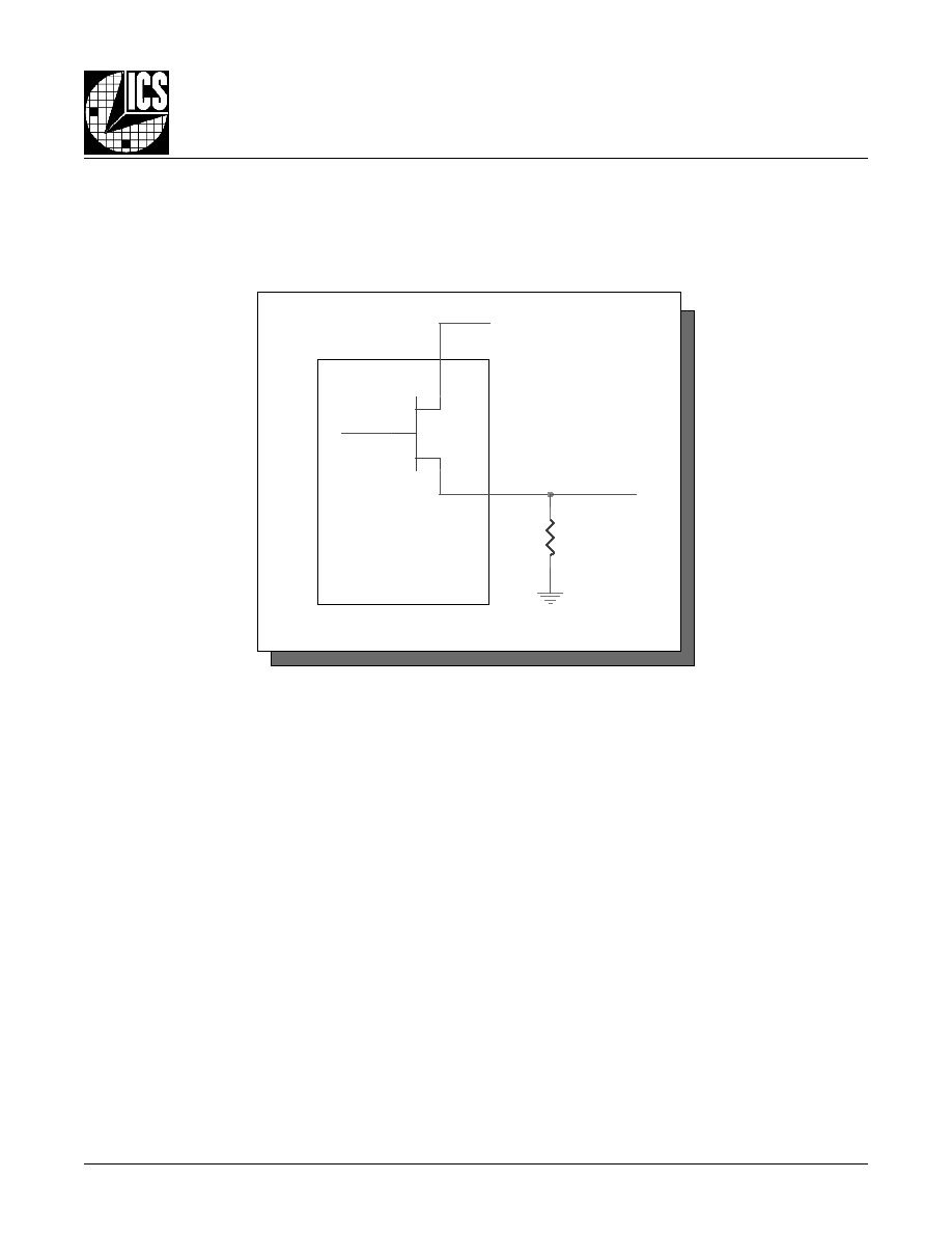
1
1
N
I
_
B
F
t
u
p
n
I
n
w
o
d
ll
u
P
.
"
y
a
l
e
d
o
r
e
z
"
h
t
i
w
s
k
c
o
l
c
g
n
i
t
a
r
e
n
e
g
e
r
r
o
f
r
o
t
c
e
t
e
d
e
s
a
h
p
o
t
t
u
p
n
i
k
c
a
b
d
e
e
F
3
1
,
2
1
9
2
,
8
2
D
N
G
r
e
w
o
P
.
d
n
u
o
r
g
y
l
p
p
u
s
r
e
w
o
P
5
1
,
4
1
0
Q
,
0
Q
n
t
u
p
t
u
O
0
5
.
s
t
u
p
t
u
o
k
c
o
l
c
l
a
i
t
n
e
r
e
f
f
i
D
.
e
c
n
a
d
e
p
m
i
t
u
p
t
u
o
l
a
c
i
p
y
t
.
s
l
e
v
e
l
e
c
a
f
r
e
t
n
i
L
T
S
H
V
L
,
7
1
,
6
1
5
2
,
4
2
V
O
D
D
r
e
w
o
P
.
s
n
i
p
y
l
p
p
u
s
t
u
p
t
u
O
9
1
,
8
1
1
Q
,
1
Q
n
t
u
p
t
u
O
0
5
.
s
t
u
p
t
u
o
k
c
o
l
c
l
a
i
t
n
e
r
e
f
f
i
D
.
e
c
n
a
d
e
p
m
i
t
u
p
t
u
o
l
a
c
i
p
y
t
.
s
l
e
v
e
l
e
c
a
f
r
e
t
n
i
L
T
S
H
V
L
1
2
,
0
2
2
Q
,
2
Q
n
t
u
p
t
u
O
0
5
.
s
t
u
p
t
u
o
k
c
o
l
c
l
a
i
t
n
e
r
e
f
f
i
D
.
e
c
n
a
d
e
p
m
i
t
u
p
t
u
o
l
a
c
i
p
y
t
.
s
l
e
v
e
l
e
c
a
f
r
e
t
n
i
L
T
S
H
V
L
3
2
,
2
2
3
Q
,
3
Q
n
t
u
p
t
u
O
0
5
.
s
t
u
p
t
u
o
k
c
o
l
c
l
a
i
t
n
e
r
e
f
f
i
D
.
e
c
n
a
d
e
p
m
i
t
u
p
t
u
o
l
a
c
i
p
y
t
.
s
l
e
v
e
l
e
c
a
f
r
e
t
n
i
L
T
S
H
V
L
7
2
,
6
2
4
Q
,
4
Q
n
t
u
p
t
u
O
0
5
.
s
t
u
p
t
u
o
k
c
o
l
c
l
a
i
t
n
e
r
e
f
f
i
D
.
e
c
n
a
d
e
p
m
i
t
u
p
t
u
o
l
a
c
i
p
y
t
.
s
l
e
v
e
l
e
c
a
f
r
e
t
n
i
L
T
S
H
V
L
0
3
V
A
D
D
r
e
w
o
P
.
n
i
p
y
l
p
p
u
s
g
o
l
a
n
A
1
3
L
E
S
_
L
L
P
t
u
p
n
I
p
u
ll
u
P
.
s
r
e
d
i
v
i
d
e
h
t
o
t
t
u
p
n
i
e
h
t
s
a
k
c
o
l
c
d
n
a
L
L
P
e
h
t
n
e
e
w
t
e
b
s
t
c
e
l
e
S
.
k
c
o
l
c
e
c
n
e
r
e
f
e
r
s
t
c
e
l
e
s
,
W
O
L
n
e
h
W
.
L
L
P
s
t
c
e
l
e
s
,
H
G
I
H
n
e
h
W
.
s
l
e
v
e
l
e
c
a
f
r
e
t
n
i
L
T
T
V
L
/
S
O
M
C
V
L
:
1
E
T
O
N
p
u
ll
u
P
d
n
a
n
w
o
d
ll
u
P
.
s
e
u
l
a
v
l
a
c
i
p
y
t
r
o
f
,
s
c
i
t
s
i
r
e
t
c
a
r
a
h
C
n
i
P
,
2
e
l
b
a
T
e
e
S
.
s
r
o
t
s
i
s
e
r
t
u
p
n
i
l
a
n
r
e
t
n
i
o
t
r
e
f
e
r
8624BYI
www.icst.com/products/hiperclocks.html
REV. A OCTOBER 8, 2002
3
Integrated
Circuit
Systems, Inc.
ICS8624I
L
OW
S
KEW
, 1-
TO
-5
D
IFFERENTIAL
-
TO
-LVHSTL Z
ERO
D
ELAY
B
UFFER
T
ABLE
2. P
IN
C
HARACTERISTICS
T
ABLE
3A. C
ONTROL
I
NPUT
F
UNCTION
T
ABLE
l
o
b
m
y
S
r
e
t
e
m
a
r
a
P
s
n
o
i
t
i
d
n
o
C
t
s
e
T
m
u
m
i
n
i
M
l
a
c
i
p
y
T
m
u
m
i
x
a
M
s
t
i
n
U
C
N
I
e
c
n
a
t
i
c
a
p
a
C
t
u
p
n
I
4
F
p
R
P
U
L
L
U
P
r
o
t
s
i
s
e
R
p
u
ll
u
P
t
u
p
n
I
1
5
K
R
N
W
O
D
L
L
U
P
r
o
t
s
i
s
e
R
n
w
o
d
ll
u
P
t
u
p
n
I
1
5
K
s
t
u
p
n
I
s
t
u
p
t
u
O
1
=
L
E
S
_
L
L
P
e
d
o
M
e
l
b
a
n
E
L
L
P
1
L
E
S
0
L
E
S
*
)
z
H
M
(
e
g
n
a
R
y
c
n
e
u
q
e
r
F
e
c
n
e
r
e
f
e
R
4
Q
n
:
0
Q
n
,
4
Q
:
0
Q
0
0
0
3
6
-
0
5
2
1
�
0
1
5
1
3
-
5
2
1
1
�
1
0
5
.
7
5
1
-
5
.
2
6
1
�
1
1
5
7
.
8
7
-
5
2
.
1
3
1
�
.
z
H
M
0
3
6
o
t
z
H
M
0
5
2
s
i
e
v
o
b
a
s
n
o
i
t
a
r
u
g
i
f
n
o
c
ll
a
r
o
f
e
g
n
a
r
y
c
n
e
u
q
e
r
f
O
C
V
:
E
T
O
N
*
s
t
u
p
n
I
s
t
u
p
t
u
O
0
=
L
E
S
_
L
L
P
e
d
o
M
s
s
a
p
y
B
L
L
P
1
L
E
S
0
L
E
S
4
Q
n
:
0
Q
n
,
4
Q
:
0
Q
0
0
4
�
0
1
4
�
1
0
4
�
1
1
8
�
T
ABLE
3B. PLL B
YPASS
F
UNCTION
T
ABLE

Integrated
Circuit
Systems, Inc.
ICS8624I
L
OW
S
KEW
, 1-
TO
-5
D
IFFERENTIAL
-
TO
-LVHSTL Z
ERO
D
ELAY
B
UFFER
8624BYI
www.icst.com/products/hiperclocks.html
REV. A OCTOBER 8, 2002
4
T
ABLE
4A. P
OWER
S
UPPLY
DC C
HARACTERISTICS
,
V
DD
= V
DDA
= 3.3V�5%, V
DDO
= 1.8V�0.2V, T
A
= -40�C
TO
85�C
l
o
b
m
y
S
r
e
t
e
m
a
r
a
P
s
n
o
i
t
i
d
n
o
C
t
s
e
T
m
u
m
i
n
i
M
l
a
c
i
p
y
T
m
u
m
i
x
a
M
s
t
i
n
U
V
D
D
e
g
a
t
l
o
V
y
l
p
p
u
S
e
r
o
C
5
3
1
.
3
3
.
3
5
6
4
.
3
V
V
A
D
D
e
g
a
t
l
o
V
y
l
p
p
u
S
g
o
l
a
n
A
5
3
1
.
3
3
.
3
5
6
4
.
3
V
V
O
D
D
e
g
a
t
l
o
V
y
l
p
p
u
S
t
u
p
t
u
O
6
.
1
8
.
1
0
.
2
V
I
D
D
t
n
e
r
r
u
C
y
l
p
p
u
S
r
e
w
o
P
0
2
1
A
m
I
A
D
D
t
n
e
r
r
u
C
y
l
p
p
u
S
g
o
l
a
n
A
5
1
A
m
I
O
D
D
t
n
e
r
r
u
C
y
l
p
p
u
S
t
u
p
t
u
O
d
a
o
L
o
N
0
A
m
A
BSOLUTE
M
AXIMUM
R
ATINGS
Supply Voltage, V
DDx
4.6V
Inputs, V
I
-0.5V to V
DD
+ 0.5V
Outputs, V
O
-0.5V to V
DDO
+ 0.5V
Package Thermal Impedance,
JA
47.9�C/W (0 lfpm)
Storage Temperature, T
STG
-65�C to 150�C
Stresses beyond those listed under Absolute Maximum Ratings may cause permanent damage to the device. These ratings
are stress specifications only. Functional operation of product at these conditions or any conditions beyond those listed in the
DC Characteristics or AC Characteristics is not implied. Exposure to absolute maximum rating conditions for extended peri-
ods may affect product reliability.
T
ABLE
4B. LVCMOS / LVTTL DC C
HARACTERISTICS
,
V
DD
= V
DDA
= 3.3V�5%, V
DDO
= 1.8V�0.2V, T
A
= -40�C
TO
85�C
l
o
b
m
y
S
r
e
t
e
m
a
r
a
P
s
n
o
i
t
i
d
n
o
C
t
s
e
T
m
u
m
i
n
i
M
l
a
c
i
p
y
T
m
u
m
i
x
a
M
s
t
i
n
U
V
H
I
e
g
a
t
l
o
V
h
g
i
H
t
u
p
n
I
2
V
D
D
3
.
0
+
V
V
L
I
e
g
a
t
l
o
V
w
o
L
t
u
p
n
I
3
.
0
-
8
.
0
V
I
H
I
t
n
e
r
r
u
C
h
g
i
H
t
u
p
n
I
,
1
L
E
S
,
0
L
E
S
R
M
,
L
E
S
_
K
L
C
V
D
D
V
=
N
I
V
5
6
4
.
3
=
0
5
1
A
�
L
E
S
_
L
L
P
V
D
D
V
=
N
I
V
5
6
4
.
3
=
5
A
�
I
L
I
t
n
e
r
r
u
C
w
o
L
t
u
p
n
I
,
1
L
E
S
,
0
L
E
S
R
M
,
L
E
S
_
K
L
C
V
D
D
V
,
V
5
6
4
.
3
=
N
I
V
0
=
5
-
A
�
L
E
S
_
L
L
P
V
D
D
V
,
V
5
6
4
.
3
=
N
I
V
0
=
0
5
1
-
A
�
T
ABLE
4C. D
IFFERENTIAL
DC C
HARACTERISTICS
,
V
DD
= V
DDA
= 3.3V�5%, V
DDO
= 1.8V�0.2V, T
A
= -40�C
TO
85�C
l
o
b
m
y
S
r
e
t
e
m
a
r
a
P
s
n
o
i
t
i
d
n
o
C
t
s
e
T
m
u
m
i
n
i
M
l
a
c
i
p
y
T
m
u
m
i
x
a
M
s
t
i
n
U
I
H
I
t
n
e
r
r
u
C
h
g
i
H
t
u
p
n
I
N
I
_
B
F
,
1
K
L
C
,
0
K
L
C
V
D
D
V
=
N
I
V
5
6
4
.
3
=
0
5
1
A
�
N
I
_
B
F
n
,
1
K
L
C
n
,
0
K
L
C
n
V
D
D
V
=
N
I
V
5
6
4
.
3
=
5
A
�
I
L
I
t
n
e
r
r
u
C
w
o
L
t
u
p
n
I
N
I
_
B
F
,
1
K
L
C
,
0
K
L
C
V
D
D
V
,
V
5
6
4
.
3
=
N
I
V
0
=
5
-
A
�
N
I
_
B
F
n
,
1
K
L
C
n
,
0
K
L
C
n
V
D
D
V
,
V
5
6
4
.
3
=
N
I
V
0
=
0
5
1
-
A
�
V
P
P
e
g
a
t
l
o
V
t
u
p
n
I
k
a
e
P
-
o
t
-
k
a
e
P
5
1
.
0
3
.
1
V
V
R
M
C
2
,
1
E
T
O
N
;
e
g
a
t
l
o
V
t
u
p
n
I
e
d
o
M
n
o
m
m
o
C
5
.
0
V
D
D
5
8
.
0
-
V
V
s
i
x
K
L
C
n
,
x
K
L
C
r
o
f
e
g
a
t
l
o
v
t
u
p
n
i
m
u
m
i
x
a
m
e
h
t
,
s
n
o
i
t
a
c
il
p
p
a
d
e
d
n
e
e
l
g
n
i
s
r
o
F
:
1
E
T
O
N
D
D
.
V
3
.
0
+
V
s
a
d
e
n
i
f
e
d
s
i
e
g
a
t
l
o
v
e
d
o
m
n
o
m
m
o
C
:
2
E
T
O
N
H
I
.

8624BYI
www.icst.com/products/hiperclocks.html
REV. A OCTOBER 8, 2002
5
Integrated
Circuit
Systems, Inc.
ICS8624I
L
OW
S
KEW
, 1-
TO
-5
D
IFFERENTIAL
-
TO
-LVHSTL Z
ERO
D
ELAY
B
UFFER
T
ABLE
6. AC C
HARACTERISTICS
,
V
DD
= V
DDA
= 3.3V�5%, V
DDO
= 1.8V�0.2V, T
A
= -40�C
TO
85�C
T
ABLE
4D. LVHSTL DC C
HARACTERISTICS
,
V
DD
= V
DDA
= 3.3V�5%, V
DDO
= 1.8V�0.2V, T
A
= -40�C
TO
85�C
l
o
b
m
y
S
r
e
t
e
m
a
r
a
P
s
n
o
i
t
i
d
n
o
C
t
s
e
T
m
u
m
i
n
i
M
l
a
c
i
p
y
T
m
u
m
i
x
a
M
s
t
i
n
U
V
H
O
;
e
g
a
t
l
o
V
h
g
i
H
t
u
p
t
u
O
1
E
T
O
N
0
.
1
4
.
1
V
V
L
O
;
e
g
a
t
l
o
V
w
o
L
t
u
p
t
u
O
1
E
T
O
N
0
4
.
0
V
V
X
O
r
e
v
o
s
s
o
r
C
t
u
p
t
u
O
e
g
a
t
l
o
V
V
(
x
%
0
4
H
O
V
-
L
O
V
+
)
L
O
V
(
x
%
0
6
H
O
V
-
L
O
V
+
)
L
O
V
V
G
N
I
W
S
k
a
e
P
-
o
t
-
k
a
e
P
g
n
i
w
S
e
g
a
t
l
o
V
t
u
p
t
u
O
6
.
0
1
.
1
V
0
5
h
t
i
w
d
e
t
a
n
i
m
r
e
t
s
t
u
p
t
u
O
:
1
E
T
O
N
.
d
n
u
o
r
g
o
t
l
o
b
m
y
S
r
e
t
e
m
a
r
a
P
s
n
o
i
t
i
d
n
o
C
t
s
e
T
m
u
m
i
n
i
M
l
a
c
i
p
y
T
m
u
m
i
x
a
M
s
t
i
n
U
f
X
A
M
y
c
n
e
u
q
e
r
F
t
u
p
t
u
O
0
3
6
z
H
M
t
D
P
1
E
T
O
N
;
y
a
l
e
D
n
o
i
t
a
g
a
p
o
r
P
z
H
M
0
3
6
4
.
3
9
.
3
5
.
4
s
n
)
�
(
t
5
,
2
E
T
O
N
;
t
e
s
f
f
O
e
s
a
h
P
c
i
t
a
t
S
V
3
.
3
=
L
E
S
_
L
L
P
5
9
-
0
3
5
5
1
s
p
t
)
o
(
k
s
5
,
3
E
T
O
N
;
w
e
k
S
t
u
p
t
u
O
0
5
s
p
t
)
c
c
(
t
ij
6
,
5
E
T
O
N
;
r
e
t
t
i
J
e
l
c
y
C
-
o
t
-
e
l
c
y
C
5
3
s
p
t
)
�
(
t
ij
6
,
5
,
4
E
T
O
N
;
r
e
t
t
i
J
e
s
a
h
P
0
5
�
s
p
t
L
e
m
i
T
k
c
o
L
L
L
P
1
s
m
t
R
e
m
i
T
e
s
i
R
t
u
p
t
u
O
%
0
8
o
t
%
0
2
0
0
3
0
0
7
s
p
t
F
e
m
i
T
ll
a
F
t
u
p
t
u
O
%
0
8
o
t
%
0
2
0
0
3
0
0
7
s
p
t
W
P
h
t
d
i
W
e
s
l
u
P
t
u
p
t
u
O
5
8
-
2
/
d
o
i
r
e
P
t
2
/
d
o
i
r
e
P
t
5
8
+
2
/
d
o
i
r
e
P
t
s
p
t
a
d
e
r
u
s
a
e
m
s
r
e
t
e
m
a
r
a
p
ll
A
f
X
A
M
.
e
s
i
w
r
e
h
t
o
d
e
t
o
n
s
s
e
l
n
u
.
t
n
i
o
p
g
n
i
s
s
o
r
c
t
u
p
t
u
o
l
a
i
t
n
e
r
e
f
f
i
d
e
h
t
o
t
t
n
i
o
p
g
n
i
s
s
o
r
c
t
u
p
n
i
l
a
i
t
n
e
r
e
f
f
i
d
e
h
t
m
o
r
f
d
e
r
u
s
a
e
M
:
1
E
T
O
N
l
a
n
g
i
s
t
u
p
n
i
k
c
a
b
d
e
e
f
d
e
g
a
r
e
v
a
e
h
t
d
n
a
k
c
o
l
c
e
c
n
e
r
e
f
e
r
t
u
p
n
i
e
h
t
n
e
e
w
t
e
b
e
c
n
e
r
e
f
f
i
d
e
m
i
t
e
h
t
s
a
d
e
n
i
f
e
D
:
2
E
T
O
N
.
e
l
b
a
t
s
s
i
y
c
n
e
u
q
e
r
f
e
c
n
e
r
e
f
e
r
t
u
p
n
i
e
h
t
d
n
a
d
e
k
c
o
l
s
i
L
L
P
e
h
t
n
e
h
w
,
s
n
o
i
t
i
d
n
o
c
ll
a
s
s
o
r
c
a
:
3
E
T
O
N
.
s
n
o
i
t
i
d
n
o
c
d
a
o
l
l
a
u
q
e
h
t
i
w
d
n
a
e
g
a
t
l
o
v
y
l
p
p
u
s
e
m
a
s
e
h
t
t
a
s
t
u
p
t
u
o
n
e
e
w
t
e
b
w
e
k
s
s
a
d
e
n
i
f
e
D
.
s
t
n
i
o
p
s
s
o
r
c
l
a
i
t
n
e
r
e
f
f
i
d
t
u
p
t
u
o
t
a
d
e
r
u
s
a
e
M
.
d
e
s
u
e
c
r
u
o
s
t
u
p
n
i
e
h
t
n
o
t
n
e
d
n
e
p
e
d
s
i
r
e
t
t
ij
e
s
a
h
P
:
4
E
T
O
N
.
5
6
d
r
a
d
n
a
t
S
C
E
D
E
J
h
t
i
w
e
c
n
a
d
r
o
c
c
a
n
i
d
e
n
i
f
e
d
s
i
r
e
t
e
m
a
r
a
p
s
i
h
T
:
5
E
T
O
N
.
z
H
M
2
2
6
f
o
y
c
n
e
u
q
e
r
f
O
C
V
t
a
d
e
z
i
r
e
t
c
a
r
a
h
C
:
6
E
T
O
N
T
ABLE
5. I
NPUT
F
REQUENCY
C
HARACTERISTICS
,
V
DD
= V
DDA
= 3.3V�5%, V
DDO
= 1.8V�0.2V, T
A
= -40�C
TO
85�C
l
o
b
m
y
S
r
e
t
e
m
a
r
a
P
s
n
o
i
t
i
d
n
o
C
t
s
e
T
m
u
m
i
n
i
M
l
a
c
i
p
y
T
m
u
m
i
x
a
M
s
t
i
n
U
f
N
I
y
c
n
e
u
q
e
r
F
t
u
p
n
I
,
0
K
L
C
n
,
0
K
L
C
1
K
L
C
n
,
1
K
L
C
1
=
L
E
S
_
L
L
P
5
2
.
1
3
0
3
6
z
H
M
0
=
L
E
S
_
L
L
P
0
3
6
z
H
M
Integrated
Circuit
Systems, Inc.
ICS8624I
L
OW
S
KEW
, 1-
TO
-5
D
IFFERENTIAL
-
TO
-LVHSTL Z
ERO
D
ELAY
B
UFFER
8624BYI
www.icst.com/products/hiperclocks.html
REV. A OCTOBER 8, 2002
6
P
ARAMETER
M
EASUREMENT
I
NFORMATION
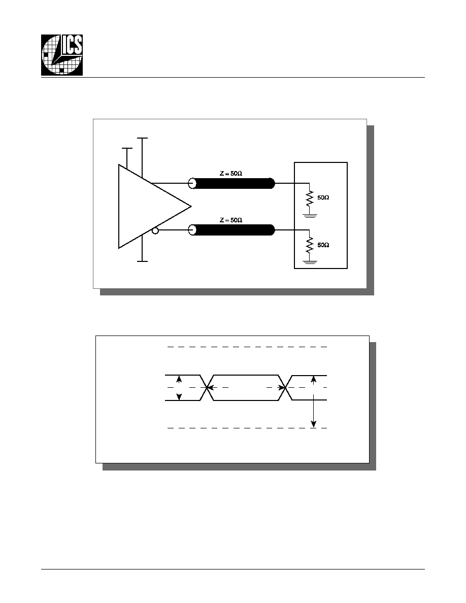
3.3V C
ORE
/1.8V O
UTPUT
L
OAD
AC T
EST
C
IRCUIT
SCOPE
LVHSTL
Qx
nQx
V
DD
, V
DDA
= 3.3V � 5%
V
DDO
= 1.8V � 0.2V
V
DDO
V
DD
, V
DDA
GND = 0V
D
IFFERENTIAL
I
NPUT
L
EVEL
V
CMR
Cross Points
V
PP
nCLK0, nCLK1
CLK0, CLK1
GND
V
DD
8624BYI
www.icst.com/products/hiperclocks.html
REV. A OCTOBER 8, 2002
7
Integrated
Circuit
Systems, Inc.
ICS8624I
L
OW
S
KEW
, 1-
TO
-5
D
IFFERENTIAL
-
TO
-LVHSTL Z
ERO
D
ELAY
B
UFFER
O
UTPUT
S
KEW
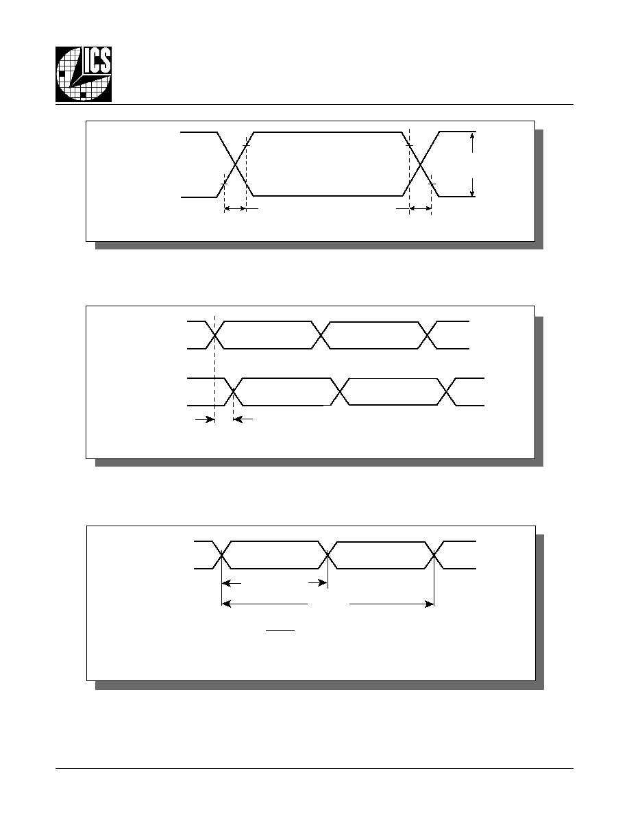
tsk(o)
nQx
Qx
nQy
Qy
Cycle-to-Cycle Jitter
t
jit(cc) =
t
cycle n �
t
cycle n+1
1000 Cycles
t
cycle n
t
cycle n+1
Q0:nQ4
nQ0:nQ4
P
HASE
J
ITTER
AND
S
TATIC
P
HASE
O
FFSET
t(�)
V
OH
V
OL
V
OH
V
OL
nCLK0, CLK1
CLK0, nCLK1
nFB_IN
FB_IN
(where
t(�) is any random sample, and t(�)
mean
is the average
of the sampled cycles measured on controlled edges)
t(�)
mean
= Static Phase Offset
tjit(�) = t(�) -- t(�)
mean
= Phase Jitter
Integrated
Circuit
Systems, Inc.
ICS8624I
L
OW
S
KEW
, 1-
TO
-5
D
IFFERENTIAL
-
TO
-LVHSTL Z
ERO
D
ELAY
B
UFFER
8624BYI
www.icst.com/products/hiperclocks.html
REV. A OCTOBER 8, 2002
8
P
ROPAGATION
D
ELAY
t
PD
nCLK0, nCLK1
CLK0, CLK1
nQ0:nQ4
Q0:Q4
odc & t
P
ERIOD
Pulse Width
t
PERIOD
t
PW
t
PERIOD
odc =
nQ0:nQ4
Q0:Q4
O
UTPUT
R
ISE
AND
F
ALL
T
IME
Clock Outputs
20%
80%
80%
20%
t
R
t
F
V
S W I N G
8624BYI
www.icst.com/products/hiperclocks.html
REV. A OCTOBER 8, 2002
9
Integrated
Circuit
Systems, Inc.
ICS8624I
L
OW
S
KEW
, 1-
TO
-5
D
IFFERENTIAL
-
TO
-LVHSTL Z
ERO
D
ELAY
B
UFFER
A
PPLICATION
I
NFORMATION
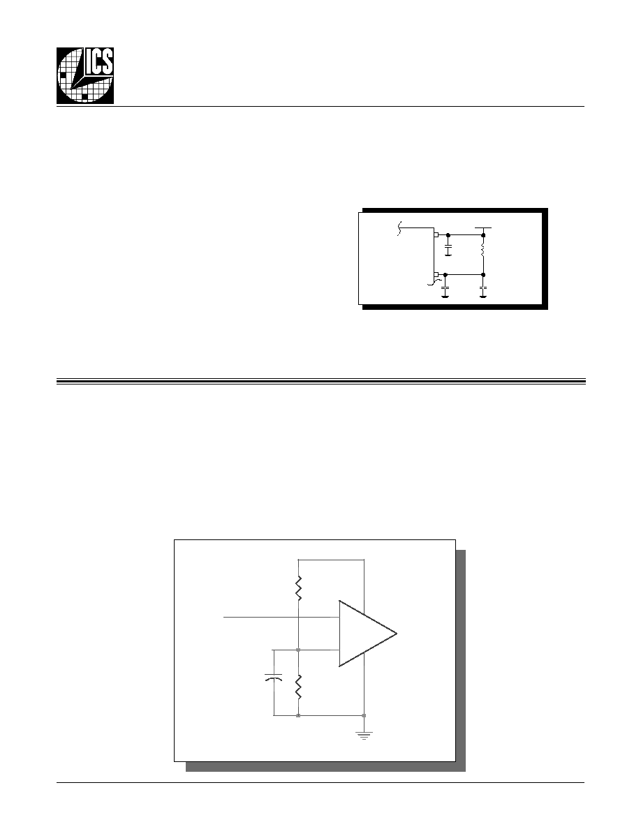
Figure 2 shows how the differential input can be wired to accept single ended levels. The reference voltage V_REF = V
DD
/2 is
generated by the bias resistors R1, R2 and C1. This bias circuit should be located as close as possible to the input pin. The ratio of
R1 and R2 might need to be adjusted to position the V_REF in the center of the input voltage swing. For example, if the input clock
swing is only 2.5V and V
DD
= 3.3V, V_REF should be 1.25V and R2/R1 = 0.609.
F
IGURE
2 - S
INGLE
E
NDED
S
IGNAL
D
RIVING
D
IFFERENTIAL
I
NPUT
R2
1K
V
DD
CLK_IN
+
-
R1
1K
C1
0.1uF
V_REF
As in any high speed analog circuitry, the power supply pins
are vulnerable to random noise. The ICS8624I provides sepa-
r a t e p o w e r s u p p l i e s t o i s o l a t e a n y h i g h s w i t c h i n g
noise from the outputs to the internal PLL. V
DD
, V
DDA
, and V
DDO
should be individually connected to the power supply
plane through vias, and bypass capacitors should be
used for each pin. To achieve optimum jitter performance,
power supply isolation is required.
Figure 1 illustrates how
a 10
resistor along with a 10
�
F and a .01
�
F bypass
capacitor should be connected to each V
DDA
pin.
P
OWER
S
UPPLY
F
ILTERING
T
ECHNIQUES
F
IGURE
1 - P
OWER
S
UPPLY
F
ILTERING
10
V
DDA
10
�
F
.01
�
F
3.3V
.01
�
F
V
DD
W
IRING
THE
D
IFFERENTIAL
I
NPUT
TO
A
CCEPT
S
INGLE
E
NDED
L
EVELS
Integrated
Circuit
Systems, Inc.
ICS8624I
L
OW
S
KEW
, 1-
TO
-5
D
IFFERENTIAL
-
TO
-LVHSTL Z
ERO
D
ELAY
B
UFFER
8624BYI
www.icst.com/products/hiperclocks.html
REV. A OCTOBER 8, 2002
10
F
IGURE
3A - ICS8624I LVHSTL Z
ERO
D
ELAY
B
UFFER
S
CHEMATIC
E
XAMPLE
L
AYOUT
G
UIDELINE
The schematic of the ICS8624I layout example is shown in
Figure 3A. The ICS8624I recommended PCB board layout for this
example is shown in
Figure 3B. This layout example is used as a general guideline. The layout in the actual system will depend on the
selected component types, the density of the components, the density of the traces, and the stacking of the P.C. board.
C11
0.01u
(U1-16)
CLK_SEL
(U1-17)
Zo = 50 Ohm
SEL1
(U1-32)
R4A
50
DIV_SEL[1:0] = 01
VDD
C4
0.1uF
Zo = 50 Ohm
R9
50
VDD=3.3V
CLK_SEL
R4B
50
C2
0.1uF
RU5
SP
VDDO=1.8V
SEL1
C7
0.1uF
VDDA
R2A
50
C1
0.1uF
RU3
1K
(U1-25)
(155.5 MHz)
VDD
R10
50
Zo = 50 Ohm
RD2
1K
R7
10
C16
10u
SP = Space (i.e. not intstalled)
R2B
50
Zo = 50 Ohm
Bypass capacitor located near the power pins
VDDO
PL
L
_
SEL
RD4
SP
155.5 MHz
SEL0
C6
0.1uF
PLL_SEL
3.3V
RU4
1K
VDD
LVHSTL_input
+
-
VDD
R8
50
(U1-24)
SEL0
RD5
1K
U1
8624
1
2
3
4
5
6
7
8
9
10
11
12
13
14
15
16
17
18
19
20
21
22
23
24
32
31
30
29
28
27
26
25
SEL0
SEL1
CLK0
nCLK0
CLK1
nCLK2
CLK_SEL
MR
VD
D
nF
B
_
I
N
FB
_
I
N
GN
D
GN
D
nQ
0
Q0
V
DDO
VDDO
nQ1
Q1
nQ2
Q2
nQ3
Q3
VDDO
VD
D
PL
L
_
SEL
V
DDA
GN
D
GN
D
Q4
nQ
4
V
DDO
VDDO
RU2
SP
RD3
SP
(U1-9)
3.3V PECL Driver
C5
0.1uF
8624BYI
www.icst.com/products/hiperclocks.html
REV. A OCTOBER 8, 2002
11
Integrated
Circuit
Systems, Inc.
ICS8624I
L
OW
S
KEW
, 1-
TO
-5
D
IFFERENTIAL
-
TO
-LVHSTL Z
ERO
D
ELAY
B
UFFER
F
IGURE
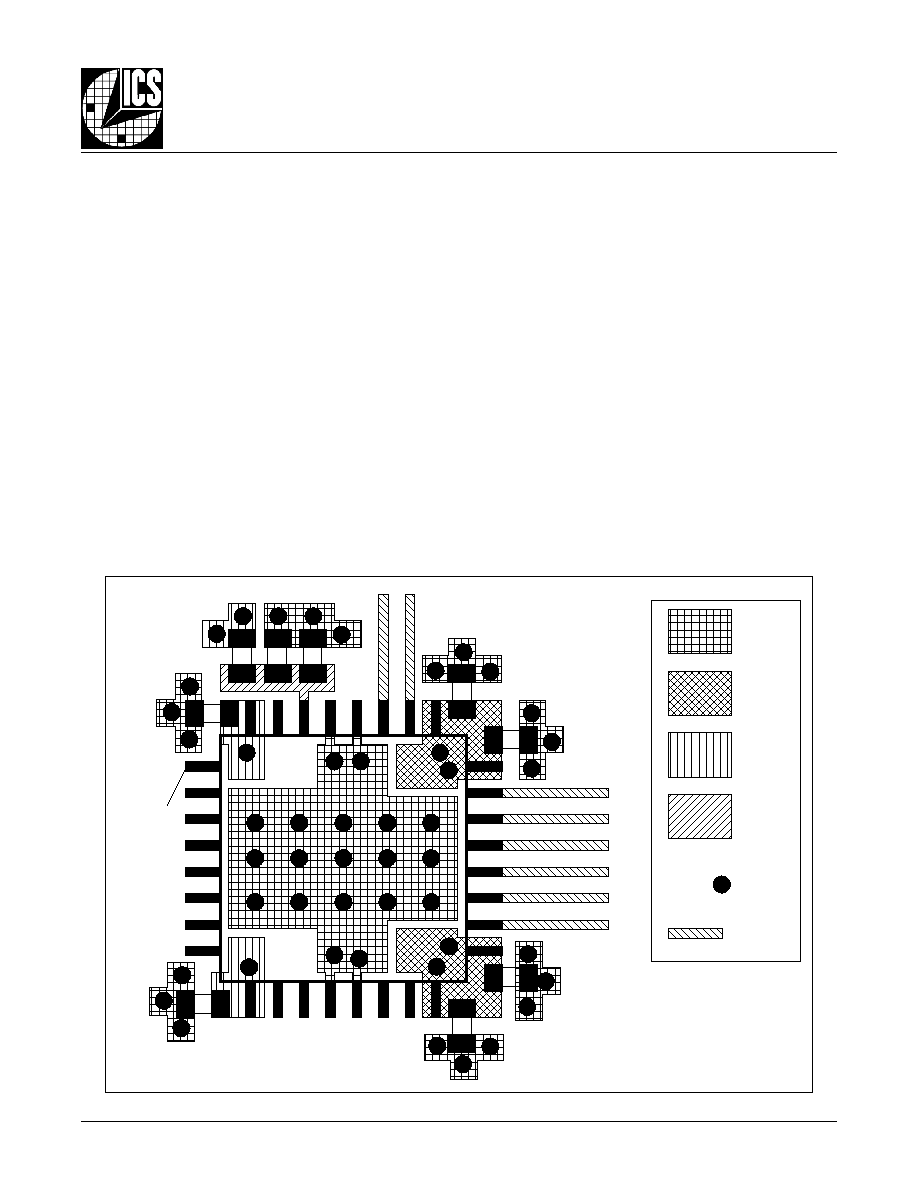
3B - PCB B
OARD
L
AYOUT
F
OR
ICS8624I
The following component footprints are used in this layout
example:
All the resistors and capacitors are size 0603.
P
OWER
AND
G
ROUNDING
Place the decoupling capacitors C1, C6, C2, C4, and C5, as
close as possible to the power pins. If space allows, placement
of the decoupling capacitor on the component side is preferred.
This can reduce unwanted inductance between the decoupling
capacitor and the power pin caused by the via.
Maximize the power and ground pad sizes and number of vias
capacitors. This can reduce the inductance between the power
and ground planes and the component power and ground pins.
The RC filter consisting of R7, C11, and C16 should be placed
as close to the V
DDA
pin as possible.
C
LOCK
T
RACES
AND
T
ERMINATION
Poor signal integrity can degrade the system performance or
cause system failure. In synchronous high-speed digital systems,
the clock signal is less tolerant to poor signal integrity than other
signals. Any ringing on the rising or falling edge or excessive ring
back can cause system failure. The shape of the trace and the
trace delay might be restricted by the available space on the board
and the component location. While routing the traces, the clock
signal traces should be routed first and should be locked prior to
routing other signal traces.
� The differential 50
output traces should have same
length.
� Avoid sharp angles on the clock trace. Sharp angle
turns cause the characteristic impedance to change on
the transmission lines.
� Keep the clock traces on the same layer. Whenever pos-
sible, avoid placing vias on the clock traces. Placement
of vias on the traces can affect the trace characteristic
impedance and hence degrade signal integrity.
� To prevent cross talk, avoid routing other signal traces in
parallel with the clock traces. If running parallel traces is
unavoidable, allow a separation of at least three trace
widths between the differential clock trace and the other
signal trace.
� Make sure no other signal traces are routed between the
clock trace pair.
� The matching termination resistors should be located as
close to the receiver input pins as possible.
GND
C1
Pin 1
50 Ohm
Traces
C11
U1
VDD
C7
C4
C5
VDDO
VDDA
C2
VIA
R7
C16
C6

Integrated
Circuit
Systems, Inc.
ICS8624I
L
OW
S
KEW
, 1-
TO
-5
D
IFFERENTIAL
-
TO
-LVHSTL Z
ERO
D
ELAY
B
UFFER
8624BYI
www.icst.com/products/hiperclocks.html
REV. A OCTOBER 8, 2002
12
P
OWER
C
ONSIDERATIONS
This section provides information on power dissipation and junction temperature for the ICS8624I.
Equations and example calculations are also provided.
1. Power Dissipation.
The total power dissipation for the ICS8624I is the sum of the core power plus the power dissipated in the load(s).
The following is the power dissipation for V
DD
= 3.3V + 5% = 3.465V, which gives worst case results.
NOTE: Please refer to Section 3 for details on calculating power dissipated in the load.
�
Power (core)
MAX
= V
DD_MAX
* I
DD_MAX
= 3.465V * 135mA = 467.8mW
�
Power (outputs)
MAX
= 32.8mW/Loaded Output pair
If all outputs are loaded, the total power is 5 * 32.8mW = 164mW
Total Power
_MAX
(3.465V, with all outputs switching) = 467.8mW + 164mW = 631.8mW
2. Junction Temperature.
Junction temperature, Tj, is the temperature at the junction of the bond wire and bond pad and directly affects the reliability of the
device. The maximum recommended junction temperature for HiPerClockS
TM
devices is 125�C.
The equation for Tj is as follows: Tj =
JA
* Pd_total + T
A
Tj = Junction Temperature
JA
= Junction-to-Ambient Thermal Resistance
Pd_total = Total Device Power Dissipation (example calculation is in section 1 above)
T
A
= Ambient Temperature
In order to calculate junction temperature, the appropriate junction-to-ambient thermal resistance
JA
must be used
. Assuming a
moderate air flow of 200 linear feet per minute and a multi-layer board, the appropriate value is 42.1�C/W per Table 7 below.
Therefore, Tj for an ambient temperature of 85�C with all outputs switching is:
85�C + 0.632W * 42.1�C/W = 111.6�C. This is well below the limit of 125�C
This calculation is only an example. Tj will obviously vary depending on the number of loaded outputs, supply voltage, air flow,
and the type of board (single layer or multi-layer).
q
JA
by Velocity (Linear Feet per Minute)
0
200
500
Single-Layer PCB, JEDEC Standard Test Boards
67.8�C/W
55.9�C/W
50.1�C/W
Multi-Layer PCB, JEDEC Standard Test Boards
47.9�C/W
42.1�C/W
39.4�C/W
NOTE: Most modern PCB designs use multi-layered boards. The data in the second row pertains to most designs.
T
ABLE
7. T
HERMAL
R
ESISTANCE
q
JA
FOR
32-
PIN
LQFP, F
ORCED
C
ONVECTION
8624BYI
www.icst.com/products/hiperclocks.html
REV. A OCTOBER 8, 2002
13
Integrated
Circuit
Systems, Inc.
ICS8624I
L
OW
S
KEW
, 1-
TO
-5
D
IFFERENTIAL
-
TO
-LVHSTL Z
ERO
D
ELAY
B
UFFER
3. Calculations and Equations.
The purpose of this section is to derive the power dissipated into the load.
LVHSTL output driver circuit and termination are shown in
Figure 4.
T
o calculate worst case power dissipation into the load, use the following equations which assume a 50
load.
Pd_H is power dissipation when the output drives high.
Pd_L is the power dissipation when the output drives low.
Pd_H = (V
OH_MAX
/R
L
) * (V
DD_MAX
- V
OH_MAX
)
Pd_L = (V
OL_MAX
/R
L
) * (V
DD_MAX
- V
OL_MAX
)
Pd_H = (1V/50
) * (2V - 1V) = 20mW
Pd_L = (0.4V/50
) * (2V - 0.4V) = 12.8mW
Total Power Dissipation per output pair = Pd_H + Pd_L = 32.8mW
F
IGURE
4 - LVHSTL D
RIVER
C
IRCUIT
AND
T
ERMINATION
V
DDO
V
OUT
RL
50
Q1

Integrated
Circuit
Systems, Inc.
ICS8624I
L
OW
S
KEW
, 1-
TO
-5
D
IFFERENTIAL
-
TO
-LVHSTL Z
ERO
D
ELAY
B
UFFER
8624BYI
www.icst.com/products/hiperclocks.html
REV. A OCTOBER 8, 2002
14
R
ELIABILITY
I
NFORMATION
T
RANSISTOR
C
OUNT
The transistor count for ICS8624I is: 1565
T
ABLE
8.
JA
VS
. A
IR
F
LOW
T
ABLE
q
JA
by Velocity (Linear Feet per Minute)
0
200
500
Single-Layer PCB, JEDEC Standard Test Boards
67.8�C/W
55.9�C/W
50.1�C/W
Multi-Layer PCB, JEDEC Standard Test Boards
47.9�C/W
42.1�C/W
39.4�C/W
NOTE: Most modern PCB designs use multi-layered boards. The data in the second row pertains to most designs.
8624BYI
www.icst.com/products/hiperclocks.html
REV. A OCTOBER 8, 2002
15
Integrated
Circuit
Systems, Inc.
ICS8624I
L
OW
S
KEW
, 1-
TO
-5
D
IFFERENTIAL
-
TO
-LVHSTL Z
ERO
D
ELAY
B
UFFER
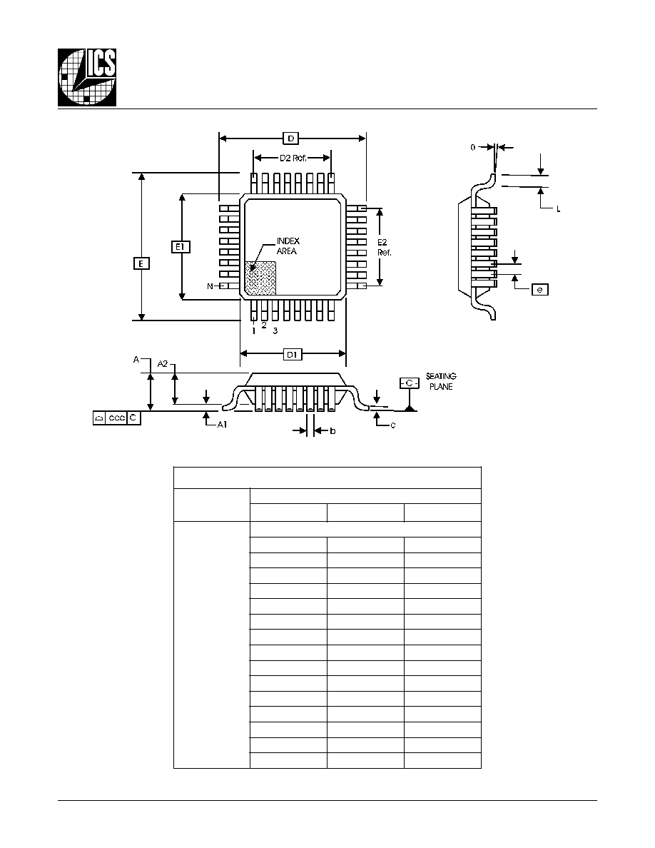
P
ACKAGE
O
UTLINE
- Y S
UFFIX
N
O
I
T
A
I
R
A
V
C
E
D
E
J
S
R
E
T
E
M
I
L
L
I
M
N
I
S
N
O
I
S
N
E
M
I
D
L
L
A
L
O
B
M
Y
S
A
B
B
M
U
M
I
N
I
M
L
A
N
I
M
O
N
M
U
M
I
X
A
M
N
2
3
A
0
6
.
1
1
A
5
0
.
0
5
1
.
0
2
A
5
3
.
1
0
4
.
1
5
4
.
1
b
0
3
.
0
7
3
.
0
5
4
.
0
c
9
0
.
0
0
2
.
0
D
C
I
S
A
B
0
0
.
9
1
D
C
I
S
A
B
0
0
.
7
2
D
0
6
.
5
E
C
I
S
A
B
0
0
.
9
1
E
C
I
S
A
B
0
0
.
7
2
E
0
6
.
5
e
C
I
S
A
B
0
8
.
0
L
5
4
.
0
0
6
.
0
5
7
.
0
q
0
�
7
�
c
c
c
0
1
.
0
T
ABLE
9. P
ACKAGE
D
IMENISIONS
Reference Document: JEDEC Publication 95, MS-026

Integrated
Circuit
Systems, Inc.
ICS8624I
L
OW
S
KEW
, 1-
TO
-5
D
IFFERENTIAL
-
TO
-LVHSTL Z
ERO
D
ELAY
B
UFFER
8624BYI
www.icst.com/products/hiperclocks.html
REV. A OCTOBER 8, 2002
16
T
ABLE
10. O
RDERING
I
NFORMATION
While the information presented herein has been checked for both accuracy and reliability, Integrated Circuit Systems, Incorporated (ICS) assumes no responsibility for either its use or
for infringement of any patents or other rights of third parties, which would result from its use. No other circuits, patents, or licenses are implied. This product is intended for use in normal
commercial and industrial applications. Any other applications such as those requiring high reliability, or other extraordinary environmental requirements are not recommended without
additional processing by ICS. ICS reserves the right to change any circuitry or specifications without notice. ICS does not authorize or warrant any ICS product for use in life support devices
or critical medical instruments.
r
e
b
m
u
N
r
e
d
r
O
/
t
r
a
P
g
n
i
k
r
a
M
e
g
a
k
c
a
P
t
n
u
o
C
e
r
u
t
a
r
e
p
m
e
T
I
Y
B
4
2
6
8
S
C
I
I
Y
B
4
2
6
8
S
C
I
P
F
Q
L
d
a
e
L
2
3
y
a
r
t
r
e
p
0
5
2
C
�
5
8
o
t
C
�
0
4
-
T
I
Y
B
4
2
6
8
S
C
I
I
Y
B
4
2
6
8
S
C
I
l
e
e
R
d
n
a
e
p
a
T
n
o
P
F
Q
L
d
a
e
L
2
3
0
0
0
1
C
�
5
8
o
t
C
�
0
4
-

8624BYI
www.icst.com/products/hiperclocks.html
REV. A OCTOBER 8, 2002
17
Integrated
Circuit
Systems, Inc.
ICS8624I
L
OW
S
KEW
, 1-
TO
-5
D
IFFERENTIAL
-
TO
-LVHSTL Z
ERO
D
ELAY
B
UFFER
T
E
E
H
S
Y
R
O
T
S
I
H
N
O
I
S
I
V
E
R
v
e
R
e
l
b
a
T
e
g
a
P
e
g
n
a
h
C
f
o
n
o
i
t
p
i
r
c
s
e
D
e
t
a
D
A
2
1
-
1
1
.
B
3
&
A
3
s
e
r
u
g
i
F
d
e
s
i
v
e
R
2
0
/
3
1
/
8
A
1
T
A
3
T
A
4
T
2
3
4
3
1
V
d
e
s
i
v
e
r
-
e
l
b
a
T
n
o
i
t
p
i
r
c
s
e
D
n
i
P
D
D
o
t
n
o
i
t
p
i
r
c
s
e
d
s
n
i
p
y
l
p
p
u
s
e
r
o
C
m
o
r
f
.
s
n
i
p
y
l
p
p
u
s
e
v
i
t
i
s
o
P
d
a
e
r
o
t
e
t
o
n
d
e
t
c
e
r
r
o
c
-
e
l
b
a
T
n
o
i
t
c
n
u
F
t
u
p
n
I
l
o
r
t
n
o
C
z
H
M
0
3
6
o
t
z
H
M
0
5
2
.
.
.
m
o
r
f
.
z
H
M
0
0
7
o
t
0
5
2
.
.
.
V
d
e
s
i
v
e
r
-
e
l
b
a
T
y
l
p
p
u
S
r
e
w
o
P
D
D
d
a
e
r
o
t
n
o
i
t
p
i
r
c
s
e
d
r
e
t
e
m
a
r
a
P
e
g
a
t
l
o
V
y
l
p
p
u
S
e
r
o
C
m
o
r
f
.
e
g
a
t
l
o
V
y
l
p
p
u
S
e
v
i
t
i
s
o
P
V
d
e
c
a
l
p
e
R
.
n
o
i
t
a
u
q
e
n
o
i
t
a
p
i
s
s
i
d
r
e
w
o
p
d
e
t
c
e
r
r
o
C
N
I
M
_
H
O
V
h
t
i
w
X
A
M
_
H
O
.
2
0
/
8
/
0
1