ChipFind - документация

Электронный компонент: ICS87931AYI

Скачать:  PDF   ZIP
ICS87931I Preliminary Datasheet
background image
87931BYI
www.icst.com/products/hiperclocks.html
REV. A JUNE 23, 2003
1
Integrated
Circuit
Systems, Inc.
ICS87931I
L
OW
S
KEW
, 1-
TO
-6
LVCMOS/LVTTL C
LOCK
M
ULTIPLIER
/Z
ERO
D
ELAY
B
UFFER
G
ENERAL
D
ESCRIPTION
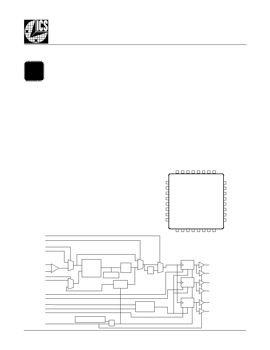
The ICS87931I is a low voltage, low skew
LVCMOS/LVTTL Clock Multiplier/ Zero Delay
Buffer and a member of the HiPerClockSTM family
of High Performance Clock Solutions from ICS.
With output frequencies up to 150MHz, the
ICS87931I is targeted for high performance clock applications.
Along with a fully integrated PLL, the ICS87931I contains fre-
quency configurable outputs and an external feedback input for
regenerating clocks with "zero delay".
Selectable clock inputs, CLK1 and differential CLK0, nCLK0
support redundant clock applications. The CLK_SEL input de-
termines which reference clock is used. The output divider val-
ues of Bank A, B and C are controlled by the DIV_SELA,
DIV_SELB and DIV_SELC, respectively.
For test and system debug purposes, the PLL_SEL input al-
lows the PLL to be bypassed. When LOW, the nMR input re-
sets the internal dividers and forces the outputs to the high im-
pedance state.
The effective fanout of the ICS87931I can be increased to 12
by utilizing the ability of each output to drive two series termi-
nated transmission lines.
F
EATURES
Fully integrated PLL
6 LVCMOS/LVTTL outputs, 7
typical output impedance
Selectable differential CLK0, nCLK0 or LVCMOS/LVTTL clock
for redundant clock applications
Maximum output frequency: 150MHz
VCO range: 220MHz to 480MHz
External feedback for "zero delay" clock regeneration
Output skew, Same Frequency: 300ps (maximum)
Output skew, Different Frequency: 400ps (maximum)
Cycle-to-cycle jitter: 100ps (maximum)
3.3V supply voltage
-40C to 85C ambient operating temperature
Pin compatible with MPC931
HiPerClockSTM
,&6
P
IN
A
SSIGNMENT
32 31 30 29 28 27 26 25
9 10 11 12 13 14 15 16
1
2
3
4
5
6
7
8
24
23
22
21
20
19
18
17
GND
QB0
QB1
V
DDO
EXTFB_SEL
CLK_SEL
PLL_SEL
nc
nc
V
DDA
POWER_DN
CLK1
nMR
CLK0
nCLK0
GND
GND
QC1
QC0
V
DDO
EXT_FB
CLK_EN1
CLK_EN0
nc
GND
QA1
QA0
V
DDO
DIV_SELA
DIV_SELB
DIV_SELC
nc
ICS87931I
32-Lead LQFP
7mm x 7mm x 1.4mm
package body
Y package
Top View
POWER_DN
PLL_SEL
CLK_SEL
CLK1
CLK0
nCLK0
EXTFB_SEL
EXT_FB
DIV_SELA
DIV_SELB
CLK_EN0
CLK_EN1
DIV_SELC
nMR
QA0
QA1
QB0
QB1
QC0
QC1
Pullup
Pulldown
Pullup
Pullup
Pullup
Pullup
Pullup
Pullup
Pullup
Pulldown
Pulldown
Pulldown
Pulldown
None
0
1
0
1
1
0
1
0
POWER-ON RESET
PHASE
DETECTOR
LPF
DISABLE
LOGIC
VCO
8
4/6
2/4
2/4
2
B
LOCK
D
IAGRAM
background image
87931BYI
www.icst.com/products/hiperclocks.html
REV. A JUNE 23, 2003
2
Integrated
Circuit
Systems, Inc.
ICS87931I
L
OW
S
KEW
, 1-
TO
-6
LVCMOS/LVTTL C
LOCK
M
ULTIPLIER
/Z
ERO
D
ELAY
B
UFFER
T
ABLE
1. P
IN
D
ESCRIPTIONS
T
ABLE
2. P
IN
C
HARACTERISTICS
r
e
b
m
u
N
e
m
a
N
e
p
y
T
n
o
i
t
p
i
r
c
s
e
D
2
3
,
7
1
,
9
,
1
c
n
d
e
s
u
n
U
.
t
c
e
n
n
o
c
o
N
2
V
A
D
D
r
e
w
o
P
.
n
i
p
y
l
p
p
u
s
g
o
l
a
n
A
3
N
D
_
R
E
W
O
P
t
u
p
n
I
p
u
ll
u
P
.
s
r
e
d
i
v
i
d
t
u
p
t
u
o
e
h
t
o
t
d
e
f
g
n
i
e
b
y
c
n
e
u
q
e
r
f
e
h
t
s
l
o
r
t
n
o
C
.
s
l
e
v
e
l
e
c
a
f
r
e
t
n
i
L
T
T
V
L
/
S
O
M
C
V
L
4
1
K
L
C
t
u
p
n
I
p
u
ll
u
P
.
s
l
e
v
e
l
e
c
a
f
r
e
t
n
i
L
T
T
V
L
/
S
O
M
C
V
L
.
t
u
p
n
i
k
c
o
l
C
5
R
M
n
t
u
p
n
I
p
u
ll
u
P
e
r
a
s
r
e
d
i
v
i
d
l
a
n
r
e
t
n
i
e
h
t
,
W
O
L
c
i
g
o
l
n
e
h
W
.
t
e
s
e
r
r
e
t
s
a
M
W
O
L
e
v
i
t
c
A
l
a
n
r
e
t
n
i
e
h
t
,
H
G
I
H
c
i
g
o
l
n
e
h
W
.
w
o
l
o
g
o
t
s
t
u
p
t
u
o
e
h
t
g
n
i
s
u
a
c
t
e
s
e
r
.
s
l
e
v
e
l
e
c
a
f
r
e
t
n
i
L
T
T
V
L
/
S
O
M
C
V
L
.
d
e
l
b
a
n
e
e
r
a
s
t
u
p
t
u
o
e
h
t
d
n
a
s
r
e
d
i
v
i
d
6
0
K
L
C
t
u
p
n
I
p
u
ll
u
P
.
t
u
p
n
i
k
c
o
l
c
l
a
i
t
n
e
r
e
f
f
i
d
g
n
i
t
r
e
v
n
i
-
n
o
N
7
0
K
L
C
n
t
u
p
n
I
/
p
u
ll
u
P
n
w
o
d
ll
u
P
V
.
t
u
p
n
i
k
c
o
l
c
l
a
i
t
n
e
r
e
f
f
i
d
g
n
i
t
r
e
v
n
I
C
C
.
g
n
i
t
a
o
l
f
t
f
e
l
n
e
h
w
t
l
u
a
f
e
d
2
/
5
2
,
4
2
,
6
1
,
8
D
N
G
r
e
w
o
P
.
d
n
u
o
r
g
y
l
p
p
u
s
r
e
w
o
P
1
1
,
0
1
,
0
N
E
_
K
L
C
1
N
E
_
K
L
C
t
u
p
n
I
p
u
ll
u
P
.
B
3
e
l
b
a
T
e
e
S
.
s
t
u
p
t
u
o
k
c
o
l
c
e
h
t
f
o
g
n
il
b
a
s
i
d
d
n
a
g
n
il
b
a
n
e
e
h
t
s
l
o
r
t
n
o
C
.
s
l
e
v
e
l
e
c
a
f
r
e
t
n
i
L
T
T
V
L
/
S
O
M
C
V
L
2
1
B
F
_
T
X
E
t
u
p
n
I
p
u
ll
u
P
.
k
c
a
b
d
e
e
f
l
a
n
r
e
t
n
i
s
t
c
e
l
e
s
,
W
O
L
n
e
h
W
.
k
c
a
b
d
e
e
f
l
a
n
r
e
t
x
E
.
s
l
e
v
e
l
e
c
a
f
r
e
t
n
i
L
T
T
V
L
/
S
O
M
C
V
L
.
B
F
_
T
X
E
s
t
c
e
l
e
s
,
H
G
I
H
n
e
h
W
8
2
,
1
2
,
3
1
V
O
D
D
r
e
w
o
P
.
s
n
i
p
y
l
p
p
u
s
t
u
p
t
u
O
5
1
,
4
1
1
C
Q
,
0
C
Q
t
u
p
t
u
O
7
.
s
t
u
p
t
u
o
k
c
o
l
c
C
k
n
a
B
.
e
c
n
a
d
e
p
m
i
t
u
p
t
u
o
l
a
c
i
p
y
t
.
s
l
e
v
e
l
e
c
a
f
r
e
t
n
i
L
T
T
V
L
/
S
O
M
C
V
L
8
1
L
E
S
_
L
L
P
t
u
p
n
I
p
u
ll
u
P
e
h
t
o
t
t
u
p
n
i
e
h
t
s
a
s
k
c
o
l
c
e
c
n
e
r
e
f
e
r
d
n
a
L
L
P
e
h
t
n
e
e
w
t
e
b
s
t
c
e
l
e
S
s
e
s
s
a
p
y
b
,
W
O
L
n
e
h
W
.
L
L
P
s
t
c
e
l
e
s
,
H
G
I
H
n
e
h
W
.
s
r
e
d
i
v
i
d
t
u
p
t
u
o
.
s
l
e
v
e
l
e
c
a
f
r
e
t
n
i
L
T
T
V
L
/
S
O
M
C
V
L
.
L
L
P
e
h
t
9
1
L
E
S
_
K
L
C
t
u
p
n
I
n
w
o
d
ll
u
P
.
e
c
n
e
r
e
f
e
R
r
o
t
c
e
t
e
D
e
s
a
h
P
e
h
t
s
t
c
e
l
e
S
.
t
u
p
n
i
t
c
e
l
e
s
k
c
o
l
C
.
1
K
L
C
s
t
c
e
l
e
s
,
H
G
I
H
n
e
h
W
.
0
K
L
C
n
,
0
K
L
C
s
t
c
e
l
e
s
,
W
O
L
n
e
h
W
.
s
l
e
v
e
l
e
c
a
f
r
e
t
n
i
L
T
T
V
L
/
S
O
M
C
V
L
0
2
L
E
S
_
B
F
T
X
E
t
u
p
n
I
n
w
o
d
ll
u
P
.
s
l
e
v
e
l
e
c
a
f
r
e
t
n
i
L
T
T
V
L
/
S
O
M
C
V
L
.
t
c
e
l
e
s
k
c
a
b
d
e
e
f
l
a
n
r
e
t
x
E
3
2
,
2
2
0
B
Q
,
1
B
Q
t
u
p
t
u
O
7
.
s
t
u
p
t
u
o
k
c
o
l
c
B
k
n
a
B
.
e
c
n
a
d
e
p
m
i
t
u
p
t
u
o
l
a
c
i
p
y
t
.
s
l
e
v
e
l
e
c
a
f
r
e
t
n
i
L
T
T
V
L
/
S
O
M
C
V
L
7
2
,
6
2
0
A
Q
,
1
A
Q
t
u
p
t
u
O
7
.
s
t
u
p
t
u
o
k
c
o
l
c
A
k
n
a
B
.
e
c
n
a
d
e
p
m
i
t
u
p
t
u
o
l
a
c
i
p
y
t
.
s
l
e
v
e
l
e
c
a
f
r
e
t
n
i
L
T
T
V
L
/
S
O
M
C
V
L
9
2
A
L
E
S
_
V
I
D
t
u
p
n
I
n
w
o
d
ll
u
P
.
A
4
e
l
b
a
T
n
i
d
e
b
i
r
c
s
e
d
s
a
A
k
n
a
B
r
o
f
s
e
u
l
a
v
r
e
d
i
v
i
d
t
u
p
t
u
o
s
e
n
i
m
r
e
t
e
D
.
s
l
e
v
e
l
e
c
a
f
r
e
t
n
i
L
T
T
V
L
/
S
O
M
C
V
L
0
3
B
L
E
S
_
V
I
D
t
u
p
n
I
n
w
o
d
ll
u
P
.
A
4
e
l
b
a
T
n
i
d
e
b
i
r
c
s
e
d
s
a
B
k
n
a
B
r
o
f
s
e
u
l
a
v
r
e
d
i
v
i
d
t
u
p
t
u
o
s
e
n
i
m
r
e
t
e
D
.
s
l
e
v
e
l
e
c
a
f
r
e
t
n
i
L
T
T
V
L
/
S
O
M
C
V
L
1
3
C
L
E
S
_
V
I
D
t
u
p
n
I
n
w
o
d
ll
u
P
.
A
4
e
l
b
a
T
n
i
d
e
b
i
r
c
s
e
d
s
a
C
k
n
a
B
r
o
f
s
e
u
l
a
v
r
e
d
i
v
i
d
t
u
p
t
u
o
s
e
n
i
m
r
e
t
e
D
.
s
l
e
v
e
l
e
c
a
f
r
e
t
n
i
L
T
T
V
L
/
S
O
M
C
V
L
:
E
T
O
N
p
u
ll
u
P
d
n
a
n
w
o
d
ll
u
P
.
s
e
u
l
a
v
l
a
c
i
p
y
t
r
o
f
,
s
c
i
t
s
i
r
e
t
c
a
r
a
h
C
n
i
P
,
2
e
l
b
a
t
e
e
S
.
s
r
o
t
s
i
s
e
r
t
u
p
n
i
l
a
n
r
e
t
n
i
o
t
r
e
f
e
r
l
o
b
m
y
S
r
e
t
e
m
a
r
a
P
s
n
o
i
t
i
d
n
o
C
t
s
e
T
m
u
m
i
n
i
M
l
a
c
i
p
y
T
m
u
m
i
x
a
M
s
t
i
n
U
C
N
I
e
c
n
a
t
i
c
a
p
a
C
t
u
p
n
I
4
F
p
R
P
U
L
L
U
P
r
o
t
s
i
s
e
R
p
u
ll
u
P
t
u
p
n
I
1
5
K
R
N
W
O
D
L
L
U
P
r
o
t
s
i
s
e
R
n
w
o
d
ll
u
P
t
u
p
n
I
1
5
K
C
D
P
e
c
n
a
t
i
c
a
p
a
C
n
o
i
t
a
p
i
s
s
i
D
r
e
w
o
P
)
t
u
p
t
u
o
r
e
p
(
V
A
D
D
V
,
O
D
D
V
5
6
4
.
3
=
2
1
F
p
R
T
U
O
e
c
n
a
d
e
p
m
I
t
u
p
t
u
O
7
background image
87931BYI
www.icst.com/products/hiperclocks.html
REV. A JUNE 23, 2003
3
Integrated
Circuit
Systems, Inc.
ICS87931I
L
OW
S
KEW
, 1-
TO
-6
LVCMOS/LVTTL C
LOCK
M
ULTIPLIER
/Z
ERO
D
ELAY
B
UFFER
T
ABLE
3B. CLK_EN
X
F
UNCTION
T
ABLE
T
ABLE
4A. VCO F
REQUENCY
F
UNCTION
T
ABLE
s
t
u
p
n
I
n
o
i
t
c
n
u
F
n
i
P
l
o
r
t
n
o
C
0
c
i
g
o
L
1
c
i
g
o
L
L
E
S
_
K
L
C
0
K
L
C
n
,
0
K
L
C
1
K
L
C
L
E
S
_
L
L
P
L
L
P
s
s
a
p
y
B
d
e
l
b
a
n
E
L
L
P
L
E
S
_
B
F
T
X
E
k
c
a
b
d
e
e
F
l
a
n
r
e
t
n
I
B
F
_
T
X
E
N
D
_
R
E
W
O
P
1
/
O
C
V
2
/
O
C
V
R
M
n
Z
i
H
t
u
p
t
u
O
/
t
e
s
e
R
r
e
t
s
a
M
s
t
u
p
t
u
O
e
l
b
a
n
E
C
L
E
S
_
V
I
D
:
A
L
E
S
_
V
I
D
)
4
(
C
Q
;
)
2
(
B
Q
;
)
2
(
A
Q
)
6
(
C
Q
;
)
4
(
B
Q
;
)
4
(
A
Q
T
ABLE
3A. C
ONTROL
I
NPUT
F
UNCTION
T
ABLE
T
ABLE
4B. I
NPUT
R
EFERENCE
F
REQUENCY
TO
O
UTPUT
F
REQUENCY
F
UNCTION
T
ABLE
(I
NTERNAL
F
EEDBACK
O
NLY
)
s
t
u
p
n
I
s
t
u
p
t
u
O
_
V
I
D
A
L
E
S
_
V
I
D
B
L
E
S
_
V
I
D
C
L
E
S
x
A
Q
x
B
Q
x
C
Q
0
=
N
D
_
R
E
W
O
P
1
=
N
D
_
R
E
W
O
P
0
=
N
D
_
R
E
W
O
P
1
=
N
D
_
R
E
W
O
P
0
=
N
D
_
R
E
W
O
P
1
=
N
D
_
R
E
W
O
P
0
0
0
2
/
O
C
V
4
/
O
C
V
2
/
O
C
V
4
/
O
C
V
4
/
O
C
V
8
/
O
C
V
0
0
1
2
/
O
C
V
4
/
O
C
V
2
/
O
C
V
4
/
O
C
V
6
/
O
C
V
2
1
/
O
C
V
0
1
0
2
/
O
C
V
4
/
O
C
V
4
/
O
C
V
8
/
O
C
V
4
/
O
C
V
8
/
O
C
V
0
1
1
2
/
O
C
V
4
/
O
C
V
4
/
O
C
V
8
/
O
C
V
6
/
O
C
V
2
1
/
O
C
V
1
0
0
4
/
O
C
V
8
/
O
C
V
2
/
O
C
V
4
/
O
C
V
4
/
O
C
V
8
/
O
C
V
1
0
1
4
/
O
C
V
8
/
O
C
V
2
/
O
C
V
4
/
O
C
V
6
/
O
C
V
2
1
/
O
C
V
1
1
0
4
/
O
C
V
8
/
O
C
V
4
/
O
C
V
8
/
O
C
V
4
/
O
C
V
8
/
O
C
V
1
1
1
4
/
O
C
V
8
/
O
C
V
4
/
O
C
V
8
/
O
C
V
6
/
O
C
V
2
1
/
O
C
V
s
t
u
p
n
I
s
t
u
p
t
u
O
_
V
I
D
A
L
E
S
_
V
I
D
B
L
E
S
_
V
I
D
C
L
E
S
x
A
Q
x
B
Q
x
C
Q
0
=
N
D
_
R
E
W
O
P
1
=
N
D
_
R
E
W
O
P
0
=
N
D
_
R
E
W
O
P
1
=
N
D
_
R
E
W
O
P
0
=
N
D
_
R
E
W
O
P
1
=
N
D
_
R
E
W
O
P
0
0
0
x
4
x
2
x
4
x
2
x
2
x
0
0
1
x
4
x
2
x
4
x
2
x
3
/
4
x
3
/
2
0
1
0
x
4
x
2
x
2
x
x
2
x
0
1
1
x
4
x
2
x
2
x
x
3
/
4
x
3
/
2
1
0
0
x
2
x
x
4
x
2
x
2
x
1
0
1
x
2
x
x
4
x
2
x
3
/
4
x
3
/
2
1
1
0
x
2
x
x
2
x
x
2
x
1
1
1
x
2
x
x
2
x
x
3
/
4
x
3
/
2
s
t
u
p
n
I
1
N
E
_
K
L
C
0
N
E
_
K
L
C
C
L
E
S
V
I
D
:
A
L
E
S
_
V
I
D
x
A
Q
x
B
Q
x
C
Q
0
0
e
l
g
g
o
T
W
O
L
W
O
L
0
1
W
O
L
W
O
L
e
l
g
g
o
T
1
0
e
l
g
g
o
T
W
O
L
e
l
g
g
o
T
1
1
e
l
g
g
o
T
e
l
g
g
o
T
e
l
g
g
o
T
background image
87931BYI
www.icst.com/products/hiperclocks.html
REV. A JUNE 23, 2003
4
Integrated
Circuit
Systems, Inc.
ICS87931I
L
OW
S
KEW
, 1-
TO
-6
LVCMOS/LVTTL C
LOCK
M
ULTIPLIER
/Z
ERO
D
ELAY
B
UFFER
VCO
VCO/2
POWER_DN
QA(2)
QB(4)
QC(6)
QA
QB
QC
CLK_EN0
CLK_EN1
QA(2)
QB(4)
QC(6)
CLK_EN0
CLK_EN1
F
IGURE
1A. POWER_DN T
IMING
D
IAGRAM
F
IGURE
1B. CLK_EN
X
T
IMING
D
IAGRAMS
background image
87931BYI
www.icst.com/products/hiperclocks.html
REV. A JUNE 23, 2003
5
Integrated
Circuit
Systems, Inc.
ICS87931I
L
OW
S
KEW
, 1-
TO
-6
LVCMOS/LVTTL C
LOCK
M
ULTIPLIER
/Z
ERO
D
ELAY
B
UFFER
l
o
b
m
y
S
r
e
t
e
m
a
r
a
P
s
n
o
i
t
i
d
n
o
C
t
s
e
T
m
u
m
i
n
i
M
l
a
c
i
p
y
T
m
u
m
i
x
a
M
s
t
i
n
U
I
N
I
t
n
e
r
r
u
C
t
u
p
n
I
0
2
1
A
V
P
P
e
g
a
t
l
o
V
t
u
p
n
I
k
a
e
P
-
o
t
-
k
a
e
P
5
1
.
0
3
.
1
V
V
R
M
C
;
e
g
a
t
l
o
V
t
u
p
n
I
e
d
o
M
n
o
m
m
o
C
2
,
1
E
T
O
N
5
.
0
+
D
N
G
V
D
D
5
8
.
0
-
V
s
n
o
i
t
a
c
il
p
p
a
d
e
d
n
e
e
l
g
n
i
s
r
o
F
:
1
E
T
O
N
,
V
s
i
0
K
L
C
n
,
0
K
L
C
r
o
f
e
g
a
t
l
o
v
t
u
p
n
i
m
u
m
i
x
a
m
e
h
t
A
D
D
.
V
3
.
0
+
s
i
e
g
a
t
l
o
v
e
d
o
m
n
o
m
m
o
C
:
2
E
T
O
N
V
s
a
d
e
n
i
f
e
d
H
I
.
T
ABLE
5C. D
IFFERENTIAL
DC C
HARACTERISTICS
,
V
DDA
= V
DDO
= 3.3V5%, T
A
= -40C
TO
85C
T
ABLE
5B. LVCMOS/LVTTL DC C
HARACTERISTICS
,
V
DDA
= V
DDO
= 3.3V5%, T
A
= -40C
TO
85C
T
ABLE
5A. P
OWER
S
UPPLY
DC C
HARACTERISTICS
,
V
DDA
= V
DDO
= 3.3V5%, T
A
= -40C
TO
85C
l
o
b
m
y
S
r
e
t
e
m
a
r
a
P
s
n
o
i
t
i
d
n
o
C
t
s
e
T
m
u
m
i
n
i
M
l
a
c
i
p
y
T
m
u
m
i
x
a
M
s
t
i
n
U
V
A
D
D
e
g
a
t
l
o
V
y
l
p
p
u
S
g
o
l
a
n
A
5
3
1
.
3
3
.
3
5
6
4
.
3
V
V
O
D
D
e
g
a
t
l
o
V
y
l
p
p
u
S
t
u
p
t
u
O
5
3
1
.
3
3
.
3
5
6
4
.
3
V
I
A
D
D
t
n
e
r
r
u
C
y
l
p
p
u
S
g
o
l
a
n
A
0
2
A
m
I
O
D
D
t
n
e
r
r
u
C
y
l
p
p
u
S
t
u
p
t
u
O
0
0
1
A
m
l
o
b
m
y
S
r
e
t
e
m
a
r
a
P
s
n
o
i
t
i
d
n
o
C
t
s
e
T
m
u
m
i
n
i
M
l
a
c
i
p
y
T
m
u
m
i
x
a
M
s
t
i
n
U
V
H
I
t
u
p
n
I
e
g
a
t
l
o
V
h
g
i
H
,
C
L
E
S
_
V
I
D
:
A
L
E
S
_
V
I
D
,
0
N
E
_
K
L
C
N
E
_
K
L
C
,
1
n
,
N
D
_
R
E
W
O
P
,
L
E
S
_
K
L
C
,
R
M
L
E
S
_
B
F
T
X
E
,
L
E
S
_
L
L
P
2
V
D
D
3
.
0
+
V
B
F
_
T
X
E
,
1
K
L
C
2
V
D
D
3
.
0
+
V
V
L
I
t
u
p
n
I
e
g
a
t
l
o
V
w
o
L
,
C
L
E
S
_
V
I
D
:
A
L
E
S
_
V
I
D
,
1
N
E
_
K
L
C
,
0
N
E
_
K
L
C
,
L
E
S
_
K
L
C
,
R
M
n
,
N
D
_
R
E
W
O
P
L
E
S
_
B
F
T
X
E
,
L
E
S
_
L
L
P
3
.
0
-
8
.
0
V
B
F
_
T
X
E
,
1
K
L
C
3
.
0
-
3
.
1
V
I
N
I
t
n
e
r
r
u
C
t
u
p
n
I
0
2
1
A
V
H
O
1
E
T
O
N
;
e
g
a
t
l
o
V
h
g
i
H
t
u
p
t
u
O
I
H
O
A
m
0
2
-
=
4
.
2
V
V
L
O
1
E
T
O
N
;
e
g
a
t
l
o
V
w
o
L
t
u
p
t
u
O
I
L
O
A
m
0
2
=
5
.
0
V
0
5
h
t
i
w
d
e
t
a
n
i
m
r
e
t
s
t
u
p
t
u
O
:
1
E
T
O
N
V
o
t
O
D
D
.
t
i
u
c
r
i
C
t
s
e
T
d
a
o
L
t
u
p
t
u
O
V
3
.
3
,
n
o
i
t
c
e
s
t
n
e
m
e
r
u
s
a
e
M
r
e
t
e
m
a
r
a
P
e
e
S
.
2
/
A
BSOLUTE
M
AXIMUM
R
ATINGS
Supply Voltage, V
DD
4.6V
Inputs, V
I
-0.5V to V
DDA
+ 0.5 V
Outputs, V
O
-0.5V to V
DDO
+ 0.5V
Package Thermal Impedance,
JA
47.9C/W (0 lfpm)
Storage Temperature, T
STG
-65C to 150C
NOTE: Stresses beyond those listed under Absolute
Maximum Ratings may cause permanent damage to the
device. These ratings are stress specifications only. Functional
operation of product at these conditions or any conditions be-
yond those listed in the
DC Characteristics or AC Character-
istics is not implied. Exposure to absolute maximum rating
conditions for extended periods may affect product reliability.

Document Outline