
Integrated
Circuit
Systems, Inc.
General Description
Features
ICS9120-46
Modem and Audio Clock Generator
9120-46 Rev B 052497P
Block Diagram
The ICS9120-46 is a high performance frequency generator
designed to support the clock requirements of communication
and audio interfaces. It offers the clock frequencies required
by 28.8 baud modem plus sound system. These frequencies
are synthesized from 14.7456 MHz reference oscillator whose
buffered output is available for the reference.
High accuracy, low-jitter PLLs meet the -96dB signal-to-
noise ratios required by 16-bit audio systems. Fast output
clock edge rates minimize board induced jitter.
The on-chip XTAL oscillator accuracy is better than ±100ppm
for an AT cut, 18pF load crystal with initial accuracy of ppm
plus TC, aging and load variation of ±20ppm each assuming
33pF ±5% external load capacitors.
∑
Generates 49.92 MHz, 40.32 MHz and 14.7456 MHz
∑
Single 14.7456 MHz crystal reference
∑
49.92 MHz accuracy tracks 40.32 MHz reference
∑
80ps one sigma jitter maintains 16-bit performance
∑
Output rise/fall times less than 1.5ns
∑
On-chip loop filter components
∑
3.0-5.5V supply range
∑
8-pin, 150-mil SOIC package
Applications
∑
Specifically designed to support the high performance
requirements of communication and audio interfaces.
ICS reserves the right to make changes in the device data identified in this
publication without further notice. ICS advises its customers to obtain the latest
version of all device data to verify that any information being relied upon by the
customer is current and accurate.
2
ICS9120-46
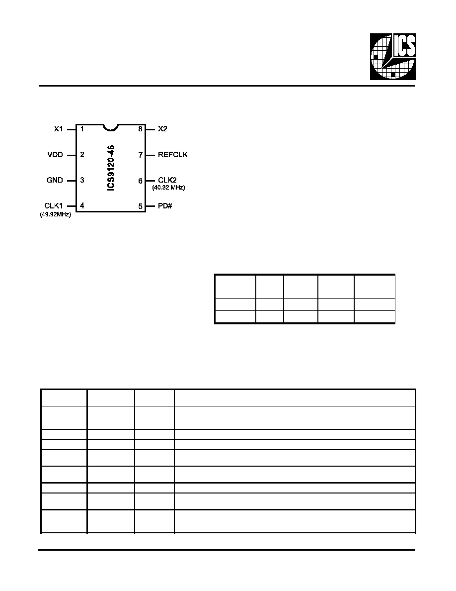
Pin Configuration
Pin Descriptions for ICS9120-46
Functionality
X1 (MHz)
PD#
CLK1
(MHz)
CLK2
(MHz)
REF
(MHa)
-
0
Low
Low
Low
14.7456
1
49.92
40.32
14.7456
8-Pin SOIC
P I N
N U M B E R
P I N
N A M E
T Y P E
D E S C R I P T I O N
1
X 1
Input
Crystal or external clock source. H as feedback bias for crystal.
N om inally 14.7456<N> M H z input applied. (N o internal load cap;
m ust connect external load cap to ground for crystal oscillator.)
2
V DD
Pow er
+Pow er supply input.
3
G ND
Pow er
G round return for Pin 2.
4
C LK1
O utput
49.92 M H z target output clock
(w ith nom inal 14.7456 M H z input).
5
PD #
O utput
Power-down input. A ll outputs shut off and driven to low output state
w hen this pin is at logic low level. H as pull-up.
6
C LK2
O utput
40.32 M H z target output clock.
7
R EF
O utput
14.7456 M Hz reference clock buffered output
(w ith nom inal 14.7456 M H z input).
8
X 2
O utput
Crystal output drive (leave this pin unconnected when using an
external clock). (N o internal load cap; m ust connect external load cap
to ground for crystal oscillator).
Functionality
The ICS9120-46 incorporates a crystal oscillator circuit designed
to provide 50% duty cycle over a range of operating conditions,
including the addition of external crystal load capacitors to pins
X1 and X2.
For the crystal oscillator, the crystal load capacitance must be
connected externally by adding a capacitor from each of the X1
and X2 pins to ground. A parallel resonant 14.7456 MHz crystal is
recommended.
Duty cycle is also maintained when using an external clock source
(connected to X1, X2 left unconnected) as long as the external
clock has good duty cycle.

3
ICS9120-46
Absolute Maximum Ratings
Electrical Characteristics at 5 V
V
DD
= +4.5 to +5.5 V, T
A
= 0 to 70
o
C unless otherwise stated
*Parameter is guaranteed by design and characterization. Not 100% tested in production.
AVDD, VDD referenced to GND .......................................................................... 7V
Operating temperature under bias .................................................... 0
o
C to +70
o
C
Storage temperature ..................................................................... -65
o
C to +150
o
C
Voltage on I/O pins referenced to GND ...................... GND -0.5V to VDD +0.5V
Power dissipation ...................................................................................... 0.5 Watts
Stresses above those listed under Absolute Maximum Ratings may cause permanent damage to the device. This is a stress
rating only and functional operation of the device at these or any other conditions above those indicated in the operational
sections of the specifications is not implied. Exposure to absolute maximum rating conditions for extended periods may
affect product reliability.
DC Characteristics
PARAMETER
SYMBOL TEST CONDITIONS
MIN
TYP
MAX
UNITS
Input Low Voltage
V
IL
-
-
0.8
V
Input High Voltage
V
IH
2.0
-
-
V
Input Low Current
I
IL
V
IN
=0V
-18.0
-8.3
-
µA
Input High Current
I
IH
V
IN
=V
DD
-
-
5.0
µA
Output Low Voltage
V
OL
IOL=+10mA
-
0.15
0.4
V
Output High Voltage
V
OH
IOH=-30mA
2.4
3.7
-
V
Output Low Current
I
OL
V
OL
=0.8V
25.0
45.0
-
mA
Output High Current
I
OH
V
OH
=2.4V
-
-53.0
-35.0
mA
Supply Current
I
DD
Unloaded
-
27.0
50.0
mA
Supply Current Power-down
I
DDPD
Unloaded; Pin 5=0V
-
500.0
800.0
µA
Pull-up Resistor Value
Rpu
-
400.0
800.0
k ohm
AC Characteristics
Rise Time
T
r
15pF load 0.8 to 2.0V
-
0.8
2.0
ns
Fall Time
T
f
*
15pF load 2.0 to 0.8V
-
0.6
1.5
ns
Rise Time
T
r
15pF load 20% to 80%
-
1.7
3.0
ns
Fall Time
T
f
15pF load 80% to 20%
-
1.1
2.5
ns
Duty Cycle
D
t
15pF load @ 50% of
VDD; Except REFCLK
45.0
50.0
55.0
%
Duty Cycle
D
t
15pF load @ 50% of
VDD; REFCLK only
40.0
45.0
60.0
%
Jitter, One Sigma
T
jis
For all frequencies
except REFCLK
-
70.0
90.0
ps
Jitter, Absolute
T
jab
For all frequencies
except REFCLK
300.0
270
300.0
ps
Jitter, One Sigma
T
jis
REFCLK only
-
350.0
500.0
ps
Jitter Absolute
T
jab
REFCLK only
-1.0
0.8
1.0
ns
Input Frequency Range
F
i
11.0
14.0
17.0
MHz
Output Frequency Range
F
o
11.0
-
58.0
MHz
Power-up Time
T
pu
0 to 40.3 MHz
-
5.5
12.0
ms
Crystal Input Capacitance
C
inx
X1 (Pin 1),X2 (Pin 8)
-
5
-
pF
4
ICS9120-46
Electrical Characteristics at 3.3 V
V
DD
= +3.0 to +3.7 V, T
A
= 0
O
C-70
o
C unless otherwise stated
*Parameter is guaranteed by design and characterization. Not 100% tested in production.
DC Characteristics
PARAMETER
SYMBOL
TEST CONDITIONS
MIN
TYP
MAX
UNITS
Input Low Voltage
V
IL
-
-
0.2V
DD
V
Input High Voltage
V
IH
0.7V
DD
-
-
V
Input Low Current
I
IL
V
IN
=0V
-8.0
-3.6
-
µ A
Input High Current
I
IH
V
IN
=VDD
-
-
5.0
µ A
Output Low Voltage
V
OL
I
OL
=6.0mA
-
0.05V
DD
1.1
V
Output High Voltage
V
OH
I
OH
=4.0mA
0.85V
DD
0.94V
DD
-
V
Output Low Current
I
OL
V
O
L=0.2V
DD
15.0
24.0
-
mA
Output High Current
I
OH
V
OH
=0.7V
DD
-
-13.0
-8.0
mA
Supply Current
I
DD
Unloaded
-
20.0
40.0
mA
Supply Current Power-
down
I
DDPD
Unloaded; Pin 5=0V
-
200.0
400.0
µ A
Pull-up Resistor Value
Rpu
-
620.0
900.0
k ohm
AC Characteristics
Rise Time
T
r
15pF load 0.8 to 2.0V
-
2.2
3.5
ns
Fall Time
T
f
*
15pF load 2.0 to 0.8V
-
1.2
2.5
ns
Rise Time
T
r
15pF load 20% to 80%
-
2.3
4.0
ns
Fall Time
T
f
15pF load 80% to 20%
-
1.2
3.0
ns
Duty Cycle
D
t
15pF load @ 50% of
VDD; Except REFCLK
45.0
50.0
55.0
%
Duty Cycle
D
t
15pF load @ 50% of
VDD; REFCLK only
40.0
45.0
60.0
%
Jitter, One Sigma
T
j1s
For all frequencies
except REFCLK
-
80.0
100.0
ps
Jitter Absolute
T
jab
For all frequencies
except REFCLK
-350.0
±300.0
350.0
ps
Jitter, One Sigma
T
j1s
REFCLK only
-
380.0
500.0
ps
Jitter, Absolute
T
jab
REFCLK only
-1.0
0.8
1.0
ns
Input Frequency Range
F
i
11.0
14.745
15.0
MHz
Output Frequency Range
F
o
14.0
-
51.0
MHz
Power-up Time
T
pu
0 to 40.3 MHz
-
5.5
12.0
ms
Crystal Input Capacitance
C
inx
X1 (Pin 1), X2 (Pin 8)
-
5
-
pF
5
ICS9120-46
Ordering Information
ICS9120M-46
ICS reserves the right to make changes in the device data identified in this
publication without further notice. ICS advises its customers to obtain the latest
version of all device data to verify that any information being relied upon by the
customer is current and accurate.
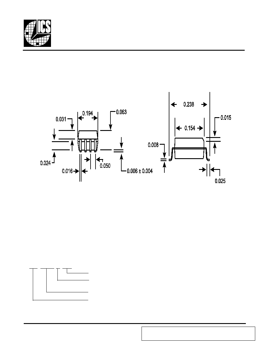
8 Pin SOIC Package
ICS XXXX M-PPP
Example:
Package Type
M=SOIC
Device Type (consists of 3 or 4 digit numbers)
ICS=Standard Device
Prefix
Pattern Number(2 or 3 digit number for parts with ROM code patterns)