Äîêóìåíòàöèÿ è îïèñàíèÿ www.docs.chipfind.ru
Integrated
Circuit
Systems, Inc.
General Description
Features
ICS9147-09
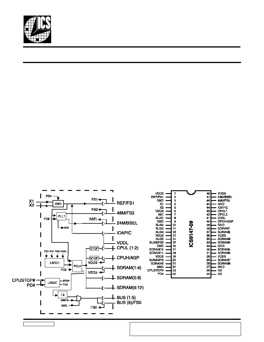
Block Diagram
Pentium is a trademark of Intel Corporation
Frequency Generator & Integrated Buffers for 686 Series CPUs
9147-09 Rev A 10/2897P
Pin Configuration
The ICS9147-09 generates all clocks required for high
speed RISC or CISC microprocessor systems such as Intel
PentiumPro, AMD or Cyrix processors. Four bidirectional I/O
pins (FS0, FS1, FS2, BSEL) are latched at power-on to the
functionality table. The Six BUS clocks can be selected as
either synchronous at 1/2 CPU speed or asynchronous at
32MHz selected by BSEL latched input.The inputs provide
for tristate and test mode conditions to aid in system level
testing.These multiplying factors can be customized for
specific applications. Glitch-free stop clock controls
provided for CPU.
High drive BUS and SDRAM outputs typically provide
greater than 1 V/ns slew rate into 30 pF loads. CPU outputs
typically provide better than 1V/ns slew rate into 20pF
loads while maintaining 50±5% duty cycle. The REF clock
outputs typically provide better than 0.5V/ns slew rates.
Seperate buffer supply pin VDDL allows for nominal 3.3V
voltage or reduced voltage swing (from 2.9 to 2.5V) for
CPUL (1:2) and IOAPIC outputs.
Total of 15 CPU speed clocks:
- Two copies of CPU clock with VDDL (2.5 to 3.3V)
- Twelve (12) SDRAM (3.3v) plus one
CPUH/AGP (3.3V) clocks
Six copies of BUS clock (synchronous with CPU clock/2 or
asynchronous 32 MHz)
250ps output skew window for CPU andSDRAM clocks
and 500ps window BUS clocks. CPU clocks to
BUSclocks skew 1-4ns (CPU early)
Two copies of Ref. clock @14.31818 MHz (One driven
by VDDL as IOAPIC)
One 48 MHz (3.3 V TTL) for USB support and single
24 MHz.
Separate VDDL for CPUL (1:2) clock buffers and
IOAPIC to allow 2.5V output (or Std. Vdd)
3.0V 3.7V supply range w/2.5V compatible outputs
48-pin SSOP package
48-Pin SSOP
ICS reserves the right to make changes in the device data identified in this
publication without further notice. ICS advises its customers to obtain the latest
version of all device data to verify that any information being relied upon by the
customer is current and accurate.
2
ICS9147-09
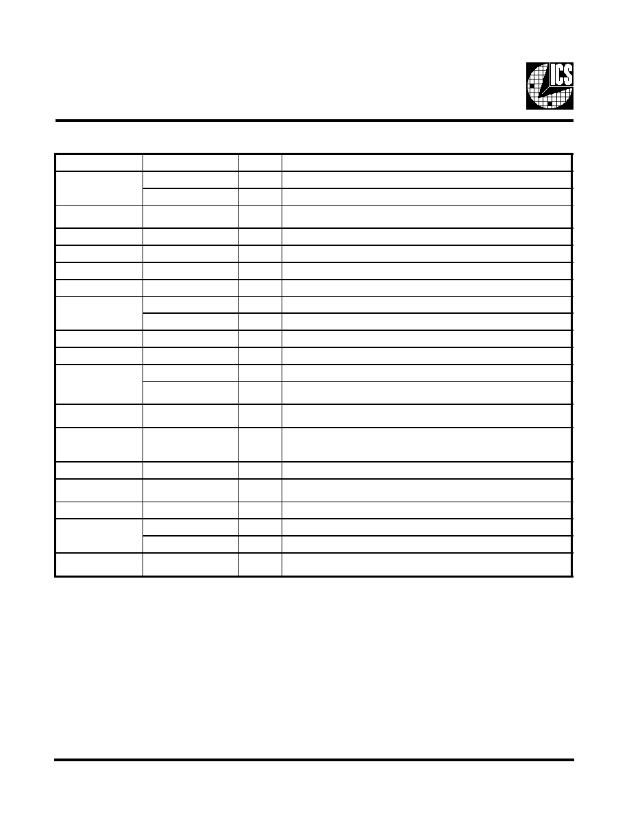
Pin Descriptions
* Bidirectional input/output pins, input logic level determined at internal power-on-reset are latched. Use 10Kohm resistor to
program logic Hi to VDD or GND for logic low.
PIN NUMBER
PIN NAME
TYPE
DESCRIPTION
2
REF
OUT
Reference clock output*
FS1
IN
Logic input frequency select Bit1*. Input latched at Poweron.
3, 9, 16, 22,
27, 33, 39, 45
GND
PWR
Ground.
4
X1
IN
Crystal input. Nominally 14.318 MHz. Has internal load cap
5
X2
OUT
Crystal output. Has internal load cap and feedack resistor to X1
41
VDDL
PWR
2.5 or 3.3V buffer power for CPUL and IOAPIC output buffers.
8, 10, 11, 12, 14,
BUS (1:5)
OUT
BUS clock outputs. see select table for frequency
15
BUS6
OUT
BUS clock output. See select table for frequency.*
FS0
IN
Logic input frequency select Bit0.*. Input latched at Poweron.
23
CPU_STOP#
IN
Halts CPU Clocks at Logic "0" level when low. Internal Pull-up
24
PD#
IN
Powers down chip, active low. Internal Pull-up
47
24M
OUT
24MHz fixed clock.*
BSEL
IN
Logic input* for selecting synchronous or asynchronous BUS
frequency- see table above. Input latched at Poweron.*
1, 6, 13, 19,
30, 36, 48
VDD3
PWR
3.3 volt core logic and buffer power
17, 18, 20, 21, 28,
29, 31, 32, 34,
35, 37, 38
SDRAM (1:12)
OUT
SDRAM clocks at CPU speed. See select table for frequency.
40
CPUH/AGP
OUT
CPU clock operates at SDRAM VDD level (3.3V nom), for AGP etc.
42, 43
CPUL (1:2)
OUT
CPU clocks .See select table for frequency. Operates at down to
2.5V controlled by VDDL pin.
7, 25, 26
N/C
--
Pins not internally connected.
46
48M
OUT
48 MHz fixed clock output*.
FS2
IN
Logic input frequency select Bit 2*. Input latched at Poweron.
44
IOAPIC
OUT
Reference clock (14.318MHz) powered by VDDL,
operating 2.5 to 3.3V.
3
ICS9147-09
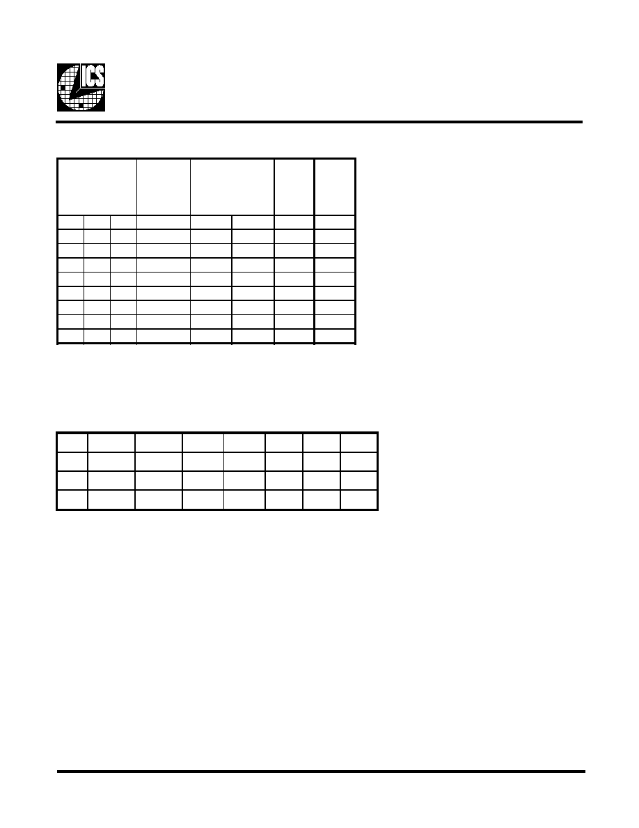
Functionality with (14.31818 MHz input)
Clock Enable Configuration
**Test: is the frequency applied to the X1 input. Can be crystal or tester generated clock overriding crystal at X1 pin.
Address Select
CPUL
(1:2)
CPUH
SDRAM
(1:12)
BUS (1:6)
(MHz)
24M
(MHz)
48M
(MHz)
FS2
FS1
FS0
(MHz)
BSEL=1
BSEL=0
(MHz)
(MHz)
0
0
0
60
30
32
24
48
0
0
1
66.8
33.4
32
24
48
0
1
0
50
25
32
24
48
0
1
1
55
27.5
32
24
48
1
0
0
75
37.5
32
24
48
1
0
1
68.5
34.3
32
24
48
1
1
0
83.3
41.65
32
24
48
1
1
1
Tristate
Tristate
Tristate
Tristate
Tristate
PD#
CPUSTOP#
CPUL (1:2)
CPUH
SDRAM
(1:12)
BUS (1:6)
24MHz
48MHz
REF
1
1
Running
Running
Running
Running
Running
Running
1
0
Stop Low
Running
Running
Running
Running
Running
0
X
Stop Low
Stop Low Stop Low Stop Low Stop Low Stop Low
4
ICS9147-09
Absolute Maximum Ratings
Electrical Characteristics at 3.3V
Supply Voltage . . . . . . . . . . . . . . . . . . . . . . . . . . 7.0 V
Logic Inputs . . . . . . . . . . . . . . . . . . . . . . . . . . . . GND 0.5 V to V
DD
+0.5 V
Ambient Operating Temperature . . . . . . . . . . . . 0°C to +70°C
Storage Temperature . . . . . . . . . . . . . . . . . . . . . . 65°C to +150°C
V
DD
= 3.0 3.7 V, T
A
= 0 70
°
C unless otherwise stated
Note 1: Parameter is guaranteed by design and characterization. Not 100% tested in production.
Stresses above those listed under Absolute Maximum Ratings may cause permanent damage to the device. These ratings are
stress specifications only and functional operation of the device at these or any other conditions above those listed in the
operational sections of the specifications is not implied. Exposure to absolute maximum rating conditions for extended
periods may affect product reliability.
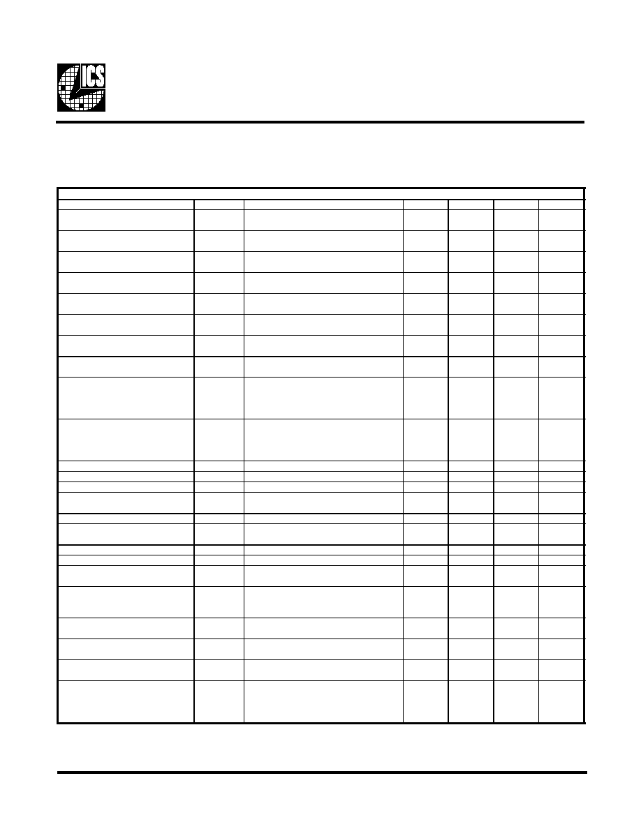
DC Characteristics
PARAMETER
SYMBOL
TEST CONDITIONS
MIN
TYP
MAX
UNITS
Input Low Voltage
V
IL
Latched inputs and Fulltime inputs
-
-
0.2V
DD
V
Input High Voltage
V
IH
Latched inputs and Fulltime inputs
0.7V
DD
-
-
V
Input Low Current
I
IL
V
IN
= 0V (Fulltime inputs)
-28.0
-10.5
-
µA
Input High Current
I
IH
V
IN
=V
DD
(Fulltime inputs)
-5.0
-
5.0
µA
Output Low Current
I
OL1a
V
OL
= 0.8V; CPU, SDRAM IOAPIC, REF,
BUS; V
DD2
= 3.3V
19.0
30.0
-
mA
I
OL1b
V
OL
= 0.8V; CPUL, IOAPIC; VDD2 = 2.5V
19.0
30.0
mA
Output High Current
I
OH1a
V
OH
= 2.0V; CPU, SDRAM IOAPIC, REF,
BUS; V
DD2
= 3.3V
-
-26.0
-16.0
mA
I
OH1b
V
OH
= 2.0V; CPUL, IOAPIC; V
DD2
= 2.5V
-12.5
-9.5
mA
Output Low Current
I
OL2
V
OL
= 0.8V; for fixed 24, 48
16.0
25.0
-
mA
Output High Current
I
OH2
V
OH
= 2.0V; for fixed 24, 48
-
-22.0
-14.0
mA
Output Low Voltage
V
OL1a
I
OL
= 10mA; CPU, SDRAM IOAPIC REF,
BUS;V
DD2
= 3.3V
-
0.3
0.4
V
V
OL1b
I
OL
= 10mA; CPUL, IOAPIC; V
DD2
=2.5V
0.3
0.4
V
Output High Voltage
V
OH1a
I
OH
= -10mA; CPU, SDRAM, IOAPIC,
REF, BUS; V
DD
= 3.3V
2.4
2.8
-
V
V
OH1b
I
OH
= -10mA; CPUL, IOAPIC; VDD2=2.5V
1.95
2.1
V
Output Low Voltage
V
OL2
I
OL
= 8mA; for fixed 24, 48MHz CLKs
-
0.3
0.4
V
Output High Voltage
V
OH2
I
OH
= -8mA; for fixed 24, 48MHz CLKs
2.4
2.8
-
V
Supply Current
I
DD
@66.6 MHz; all outputs unloaded
-
120
180
mA
Power Down Current
I
pd
PD#=0
-
5.0
20.0
µA
Pull-up Resistor
R
pu
CPUSTOP#; PD#
20
40
80
Kohms
5
ICS9147-09
Electrical Characteristics at 3.3V
V
DD
= 3.0 3.7 V, T
A
= 0 70
°
C unless otherwise stated
Note 1: Parameter is guaranteed by design and characterization. Not 100% tested in production.
AC Characteristics
PARAMETER
SYMBOL
TEST CONDITIONS
MIN
TYP
MAX
UNITS
Rise Time
1
Tr1
20pF load, 0.8 to 2.0V
CPU, SDRAM, BUS & REF
-
0.9
1.5
ns
Fall Time
1
Tf1
20pF load, 2.0 to 0.8V
CPU, SDRAM, BUS & REF
-
0.8
1.4
ns
Rise Time
1
Tr3
20pF load, 0.8 to 2.0V
fixed 20 & 48 clocks
-
0.9
1.5
ns
Fall Time
1
Tf3
20pF load, 2.0 to 0.8V
fixed 20 & 48 clocks
-
1.1
1.5
ns
Rise Time
1
Tr4
20pF load, 0.4 to 2.0V , CPUL with
VDDL = 2.5V
-
2.0
2.5
ns
Fall Time
1
Tf4
20pF load, 2.0 to 0.4V, CPUL with
VDDL = 2.5V
-
1.6
2.5
ns
Duty Cycle
1
Dt
20pF load @ VOUT=1.4V
All clocks except 48MHz and REF
47
52
57
%
Duty Cycle
1
DT2
20pF load @ VOUT=1.4V
48MHz and REF outputs
40
50
60
%
Jitter, One Sigma
1
Tjis1
CPU & BUS Clocks; Load=20pF,
SDRAM; Load = 30pF, VDDL = 3.3
or 2.5V
FOUT=25 MHz, BSEL=1
-
50
150
ps
Jitter, Absolute
1
Tjab1
CPU & BUS Clocks; Load=20pF,
SDRAM; Load = 30pF, VDDL = 3.3
or 2.5V
FOUT
25 MHz, BSEL=1
-250
-
250
ps
Jitter, One Sigma
1
Tjis2
Fixed CLK; Load=20pF
-
1
3
%
Jitter, Absolute
1
Tjab2
Fixed CLK; Load=20pF
-5
2
5
%
Jitter, Cycle to Cycle
1
Tcc1
CPU Clocks, Load=20pF BSEL=1
-
250
ps
Jitter, Cycle to Cycle
1
Tcc2
CPU Clocks, Load=20pF BSEL=1
VDDL=2.5V
-
350
ps
Input Frequency
1
Fi
12.0
14.318
16.0
MHz
Ratio of nominal to output
frequency
Fout1
With input driven at 14.31818MHz to
20.0, 48.0MHz
-1
-0.1
+1
ppm
Logic Input Capacitance
1
CIN
Logic input pins
-
5
-
pF
Crystal Oscillator Capacitance
1 , 2
CINX
X1, X2 pins
2
4
6
pF
Power-on Time
1
ton
From VDD=1.6V to 1st crossing of
66.6 MHz VDD supply ramp < 40ms
-
2.5
4.5
ms
Clock Skew Window
1
Tsk1
CPU to CPU or SDRAM;
Load=20pF; @1.4V
(Same VDD)
-
150
250
ps
Clock Skew Window
1
Tsk2
BUS to BUS, SDRAM to SDRAM;
Load=20pF; @1.4V
-
300
500
ps
Clock Skew Window
1
Tsk3
CPU to BUS; Load=20pF; @1.4V
(CPU is early)
1.6
2.1
4.6
ns
Clock Skew Window
1
Tsk4
CPUL to BUS, VDDL=2.5V
Vth=1.25, CPUL (BUS Vth=1.4V)
0.50
1.50
3.0
ns
Clock Skew Window
1
Tsk5
SDRAM, CPUH (@3.3V, Vth=1.4V)
to CPUL (@2.5V Vth=1.25V)
Load=20pF
(2.5V CPUL is late)
100
600
850
ps