Äîêóìåíòàöèÿ è îïèñàíèÿ www.docs.chipfind.ru
Integrated
Circuit
Systems, Inc.
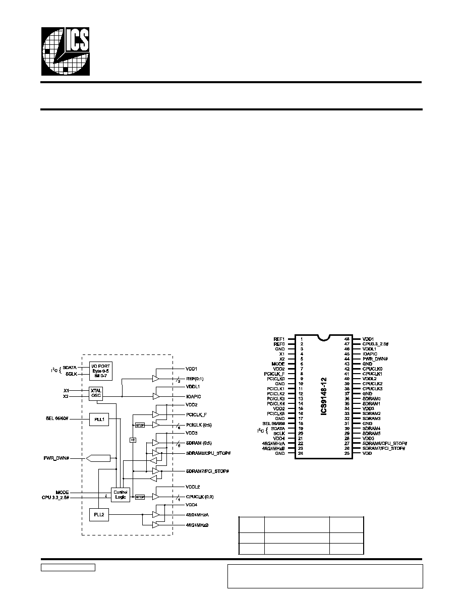
General Description
Features
ICS9148-12
Block Diagram
Pentium/Pro
TM
System Clock Chip
9148-12 Rev F 4/1/99
Pentium is a trademark on Intel Corporation.
CPU outputs are stronger drive for multiple loads per pin
(ie CPU and NB on one pin)
Generates system clocks for CPU, IOAPIC, SDRAM,
PCI, plus 14.314 MHz REF(0:1), USB, Plus Super I/O
Supports single or dual processor systems
I
2
C serial configuration interface provides output clock
disabling and other functions
MODE input pin selects optional power management
input control pins
Two fixed outputs separately selectable as 24 or 48MHz
Separate 2.5V and 3.3V supply pins
2.5V or 3.3V outputs: CPU, IOAPIC
3.3V outputs: SDRAM, PCI, REF, 48/24 MHz
CPU 3.3_2.5# logic pin to adjust output strength
No power supply sequence requirements
Uses external 14.318MHz crystal
48 pin 300 mil SSOP and 240 mil TSSOP
Output enable register
for serial port control:
1 = enable
0 = disable
The ICS9148-12 is a Clock Synthesizer chip for Pentium and
PentiumPro CPU based Desktop/Notebook systems that will
provide all necessary clock timing.
Features include four strong CPU, seven PCI and eight
SDRAM clocks. Two reference outputs are available equal to
the crystal frequency. Stronger drive CPUCLK outputs
typically provide greater than 1 V/ns slew rate into 20pF
loads. This device meets rise and fall requirements with 2
loads per CPU output (ie, one clock to CPU and NB chipset,
one clock to two L2 cache inputs).
PWR_DWN# pin allows low power mode by stopping crystal
OSC and PLL stages. For optional power management,
CPU_STOP# can stop CPU (0:3) clocks and PCI_STOP#
will stop PCICLK (0:5) clocks. CPU and IOAPIC output
buffer strength controlled by CPU 3.3_2.5# pin to match
VDDL voltage.
PCICLK outputs typically provide better than 1V/ns slew rate
into 30pF loads while maintaining 50±5% duty cycle. The REF
clock outputs typically provide better than 0.5V/ns slew rates.
The ICS9148-12 accepts a 14.318MHz reference crystal or
clock as its input and runs on a 3.3V core supply.
Functionality
VDD (1:4) 3.3V±10%, VDDL1, 2 2.5±5% or 3.3±10% 0-70
°
C
Crystal (X1, X2) = 14.31818 MHz
L
E
S
M
A
R
D
S
,
K
L
C
U
P
C
)
z
H
M
(
K
L
C
I
C
P
)
z
H
M
(
0
0
6
0
3
1
6
.
6
6
3
.
3
3
Pin Configuration
48-Pin SSOP & TSSOP
ICS reserves the right to make changes in the device data identified in this
publication without further notice. ICS advises its customers to obtain the latest
version of all device data to verify that any information being relied upon by the
customer is current and accurate.
2
ICS9148-12
Pin Descriptions
Power Groups
VDD = Supply for PLL core
VDD1 = REF (0:1), X1, X2
VDD2 = PCICLK_F, PCICLK (0:5)
VDD3 = SDRAM (0:5), SDRAM6/CPU_STOP#, SDRAM7/PCI_STOP#
VDD4 = 48/24MHzA, 48/24MHzB
VDDL1 = IOAPIC
VDDL2 = CPUCLK (0:3)
R
E
B
M
U
N
N
I
P
E
M
A
N
N
I
P
E
P
Y
T
N
O
I
T
P
I
R
C
S
E
D
1
,
2
)
1
:
0
(
F
E
R
T
U
O
t
u
p
t
u
O
k
c
o
l
c
e
c
n
e
r
e
f
e
R
,
4
2
,
7
1
,
0
1
,
3
3
4
,
7
3
,
1
3
D
N
G
R
W
P
)
n
o
m
m
o
c
(
d
n
u
o
r
G
4
1
X
N
I
p
a
c
d
a
o
l
l
a
t
s
y
r
c
l
a
n
r
e
t
n
i
s
a
h
,
t
u
p
n
i
e
c
n
e
r
e
f
e
r
r
o
l
a
t
s
y
r
C
5
2
X
T
U
O
k
c
a
b
d
e
e
f
d
n
a
p
a
c
d
a
o
l
l
a
n
r
e
t
n
i
s
a
h
,
t
u
p
t
u
o
l
a
t
s
y
r
C
1
X
o
t
r
o
t
s
i
s
e
r
6
E
D
O
M
N
I
n
o
i
t
c
e
l
e
s
n
o
i
t
c
n
u
f
t
u
p
n
I
5
1
,
7
2
D
D
V
R
W
P
V
3
.
3
l
a
n
i
m
o
n
,
)
5
:
0
(
K
L
C
I
C
P
,
F
_
K
L
C
I
C
P
r
o
f
y
l
p
p
u
S
8
F
_
K
L
C
I
C
P
T
U
O
#
P
O
T
S
_
I
C
P
y
b
d
e
t
c
e
f
f
a
t
o
n
,
k
c
o
l
c
I
C
P
g
n
i
n
n
u
r
e
e
r
F
6
1
,
4
1
,
3
1
,
2
1
,
1
1
,
9
)
5
:
0
(
K
L
C
I
C
P
T
U
O
s
k
c
o
l
c
I
C
P
8
1
#
0
6
/
6
6
L
E
S
N
I
U
P
C
d
n
a
M
A
R
D
S
r
o
f
z
H
M
6
.
6
6
r
o
z
H
M
0
6
s
t
c
e
l
e
S
9
1
A
T
A
D
S
N
I
I
2
t
u
p
n
i
a
t
a
d
C
0
2
K
L
C
S
N
I
I
2
t
u
p
n
i
k
c
o
l
c
C
1
2
4
D
D
V
R
W
P
V
3
.
3
l
a
n
i
m
o
n
,
B
z
H
M
4
2
/
8
4
,
A
z
H
M
4
2
/
8
4
r
o
f
y
l
p
p
u
S
2
2
A
z
H
M
4
2
/
8
4
T
U
O
O
/
I
r
e
p
u
S
r
o
B
S
U
r
o
f
t
u
p
t
u
o
r
e
v
i
r
d
z
H
M
4
2
/
8
4
3
2
B
z
H
M
4
2
/
8
4
T
U
O
O
/
I
r
e
p
u
S
r
o
B
S
U
r
o
f
t
u
p
t
u
o
r
e
v
i
r
d
z
H
M
4
2
/
8
4
5
2
D
D
V
R
W
P
V
3
.
3
l
a
n
i
m
o
n
,
e
r
o
c
L
L
P
r
o
f
y
l
p
p
u
S
6
2
7
M
A
R
D
S
T
U
O
)
d
e
t
c
e
l
e
s
(
z
H
M
6
.
6
6
/
0
6
k
c
o
l
c
M
A
R
D
S
#
P
O
T
S
_
I
C
P
N
I
w
o
l
n
e
h
w
l
e
v
e
l
"
0
"
c
i
g
o
l
t
a
)
5
:
0
(
s
u
B
I
C
P
s
t
l
a
H
7
2
6
M
A
R
D
S
T
U
O
)
d
e
t
c
e
l
e
s
(
z
H
M
6
.
6
6
/
0
6
k
c
o
l
c
M
A
R
D
S
#
P
O
T
S
_
U
P
C
N
I
w
o
l
n
e
h
w
l
e
v
e
l
"
0
"
c
i
g
o
l
t
a
s
k
c
o
l
c
U
P
C
s
t
l
a
H
4
3
,
8
2
3
D
D
V
R
W
P
,
#
P
O
T
S
_
U
P
C
/
6
M
A
R
D
S
,
)
5
:
0
(
M
A
R
D
S
r
o
f
y
l
p
p
u
S
V
3
.
3
l
a
n
i
m
o
n
,
#
P
O
T
S
_
I
C
P
/
7
M
A
R
D
S
0
4
2
L
D
D
V
R
W
P
l
a
n
i
m
o
n
V
3
.
3
r
o
5
.
2
r
e
h
t
i
e
,
)
3
:
0
(
K
L
C
U
P
C
r
o
f
y
l
p
p
u
S
8
3
,
9
3
,
1
4
,
2
4
)
3
:
0
(
K
L
C
U
P
C
T
U
O
2
L
D
D
V
y
b
d
e
r
e
w
o
p
,
t
u
p
t
u
o
k
c
o
l
c
K
L
C
U
P
C
9
2
,
0
3
,
2
3
,
3
3
,
5
3
,
6
3
)
5
:
0
(
M
A
R
D
S
T
U
O
)
d
e
t
c
e
l
e
s
(
z
H
M
6
.
6
6
r
o
0
6
t
a
k
c
o
l
c
s
M
A
R
D
S
4
4
#
N
W
D
_
R
W
P
N
I
w
o
l
e
v
i
t
c
a
,
p
i
h
c
n
w
o
d
s
r
e
w
o
P
5
4
C
I
P
A
O
I
T
U
O
1
L
D
D
V
y
b
d
e
r
e
w
o
p
)
z
H
M
8
1
3
.
4
1
(
,
t
u
p
t
u
o
k
c
o
l
c
C
I
P
A
O
I
6
4
1
L
D
D
V
R
W
P
l
a
n
i
m
o
n
V
3
.
3
r
o
5
.
2
r
e
h
t
i
e
,
C
I
P
A
O
I
r
o
f
y
l
p
p
u
S
7
4
#
5
.
2
-
3
.
3
U
P
C
N
I
,
D
D
V
o
t
p
u
l
l
u
p
s
a
h
,
n
o
i
t
c
e
l
e
s
h
t
g
n
e
r
t
s
r
e
f
f
u
b
D
D
V
5
.
2
r
o
3
.
3
.
r
o
t
s
i
s
e
r
K
0
3
l
a
n
i
m
o
n
8
4
1
D
D
V
R
W
P
V
3
.
3
l
a
n
i
m
o
n
,
2
X
,
1
X
,
)
1
:
0
(
F
E
R
r
o
f
y
l
p
p
u
S
3
ICS9148-12
Power-On Conditions
Example:
a) if MODE = 1, pins 26 and 27 are configured as SDRAM7 and SDRAM6 respectively.
b) if MODE = 0, pins 26 and 27 are configured as PCI_STOP# and CPU_STOP# respectively.
Power-On Default Conditions
At power-up and before device programming, all clocks will default to an enabled and on condition. The frequencies that are then produced
are on the MODE pin as shown in the table below.
K
C
O
L
C
P
U
-
R
E
W
O
P
T
A
N
O
I
T
I
D
N
O
C
T
L
U
A
F
E
D
)
1
:
0
(
F
E
R
z
H
M
8
1
8
1
3
.
4
1
0
C
I
P
A
O
I
z
H
M
8
1
8
1
3
.
4
1
z
H
M
4
2
/
8
4
z
H
M
8
4
#
0
6
/
6
6
L
E
S
E
D
O
M
#
N
I
P
N
O
I
T
P
I
R
C
S
E
D
N
O
I
T
C
N
U
F
1
1
2
4
,
1
4
,
9
3
,
8
3
s
K
L
C
U
P
C
e
l
b
a
s
i
d
/
e
l
b
a
n
e
g
i
f
n
o
c
l
a
i
r
e
s
/
w
-
z
H
M
6
.
6
6
,
2
3
,
3
3
,
5
3
,
6
3
6
2
,
7
2
,
9
2
,
0
3
M
A
R
D
S
s
t
u
p
t
u
o
M
A
R
D
S
l
l
A
-
z
H
M
6
.
6
6
,
2
1
,
3
1
,
4
1
,
6
1
8
,
9
,
1
1
s
K
L
C
I
C
P
e
l
b
a
s
i
d
/
e
l
b
a
n
e
g
i
f
n
o
c
l
a
i
r
e
s
/
w
-
z
H
M
3
.
3
3
0
1
2
4
,
1
4
,
9
3
,
8
3
s
K
L
C
U
P
C
e
l
b
a
s
i
d
/
e
l
b
a
n
e
g
i
f
n
o
c
l
a
i
r
e
s
/
w
-
z
H
M
0
6
,
2
3
,
3
3
,
5
3
,
6
3
6
2
,
7
2
,
9
2
,
0
3
M
A
R
D
S
e
l
b
a
s
i
d
/
e
l
b
a
n
e
g
i
f
n
o
c
l
a
i
r
e
s
/
w
-
z
H
M
0
6
,
2
1
,
3
1
,
4
1
,
6
1
8
,
9
,
1
1
s
K
L
C
I
C
P
e
l
b
a
s
i
d
/
e
l
b
a
n
e
g
i
f
n
o
c
l
a
i
r
e
s
/
w
-
z
H
M
0
3
1
0
6
2
#
P
O
T
S
_
I
C
P
s
k
c
o
l
C
)
5
:
0
(
I
C
P
,
t
n
e
m
e
g
a
n
a
M
r
e
w
o
P
w
o
l
n
e
h
w
d
e
p
p
o
t
S
7
2
#
P
O
T
S
_
U
P
C
s
k
c
o
l
C
)
5
:
0
(
U
P
C
,
t
n
e
m
e
g
a
n
a
M
r
e
w
o
P
w
o
l
n
e
h
w
d
e
p
p
o
t
S
8
F
_
K
L
C
I
C
P
r
o
f
g
n
i
n
n
u
r
e
e
r
F
k
c
o
l
C
I
C
P
-
z
H
M
3
.
3
3
-
z
H
M
3
.
3
3
t
n
e
m
e
g
a
n
a
M
r
e
w
o
P
2
4
,
1
4
,
9
3
,
8
3
s
K
L
C
U
P
C
d
n
a
l
o
r
t
n
o
C
p
o
t
S
l
a
n
r
e
t
x
e
/
w
s
k
c
o
l
C
U
P
C
-
z
H
M
6
.
6
6
.
e
l
b
a
s
i
d
/
e
l
b
a
n
e
l
a
u
d
i
v
i
d
n
i
g
i
f
n
o
c
l
a
i
r
e
s
,
2
3
,
3
3
,
5
3
,
6
3
9
2
,
0
3
M
A
R
D
S
l
a
u
d
i
v
i
d
n
i
g
i
f
n
o
c
l
a
i
r
e
s
/
w
s
k
c
o
l
C
M
A
R
D
S
-
z
H
M
6
.
6
6
.
e
l
b
a
s
i
d
/
e
l
b
a
n
e
,
2
1
,
3
1
,
4
1
,
6
1
9
,
1
1
s
K
L
C
I
C
P
d
n
a
l
o
r
t
n
o
c
p
o
t
S
l
a
n
r
e
t
x
e
/
w
s
k
c
o
l
C
I
C
P
-
z
H
M
3
.
3
3
.
e
l
b
a
s
i
d
/
e
l
b
a
n
e
l
a
u
d
i
v
i
d
n
i
g
i
f
n
o
c
l
a
i
r
e
s
0
0
6
2
#
P
O
T
S
_
I
C
P
s
k
c
o
l
C
)
5
:
0
(
I
C
P
,
t
n
e
m
e
g
a
n
a
M
r
e
w
o
P
w
o
l
n
e
h
w
d
e
p
p
o
t
S
7
2
#
P
O
T
S
_
U
P
C
s
k
c
o
l
C
)
5
:
0
(
U
P
C
,
t
n
e
m
e
g
a
n
a
M
r
e
w
o
P
w
o
l
n
e
h
w
d
e
p
p
o
t
S
8
F
_
K
L
C
I
C
P
r
e
w
o
P
r
o
f
g
n
i
n
n
u
r
e
e
r
F
k
c
o
l
C
I
C
P
-
z
H
M
0
3
t
n
e
m
e
g
a
n
a
M
2
4
,
1
4
,
9
3
,
8
3
s
K
L
C
U
P
C
d
n
a
l
o
r
t
n
o
c
p
o
t
S
l
a
n
r
e
t
x
e
/
w
s
k
c
o
l
C
U
P
C
-
z
H
M
0
6
.
e
l
b
a
s
i
d
/
e
l
b
a
n
e
l
a
u
d
i
v
i
d
n
i
g
i
f
n
o
c
l
a
i
r
e
s
,
2
3
,
3
3
,
5
3
,
6
3
9
2
,
0
3
M
A
R
D
S
l
a
u
d
i
v
i
d
n
i
g
i
f
n
o
c
l
a
i
r
e
s
/
w
s
k
c
o
l
C
M
A
R
D
S
-
z
H
M
0
6
.
e
l
b
a
s
i
d
/
e
l
b
a
n
e
,
2
1
,
3
1
,
4
1
,
6
1
9
,
1
1
s
K
L
C
I
C
P
d
n
a
l
o
r
t
n
o
c
p
o
t
S
l
a
n
r
e
t
x
e
/
w
s
k
c
o
l
C
I
C
P
-
z
H
M
0
3
.
e
l
b
a
s
i
d
/
e
l
b
a
n
e
l
a
u
d
i
v
i
d
n
i
g
i
f
n
o
c
l
a
i
r
e
s

4
ICS9148-12
Technical Pin Function Descriptions
VDD(1,2,3,4)
This is the power supply to the internal core logic of the
device as well as the clock output buffers for REF(0:1),
PCICLK, 48/24MHzA/B and SDRAM(0:7).
This pin operates at 3.3V volts. Clocks from the listed
buffers that it supplies will have a voltage swing from Ground
to this level. For the actual guaranteed high and low voltage
levels for the Clocks, please consult the DC parameter table
in this data sheet.
VDDL1,2
This is the power supplies for the CPUCLK and IOAPCI
output buffers. The voltage level for these outputs may be
2.5 or 3.3volts. Clocks from the buffers that each supplies
will have a voltage swing from Ground to this level. For the
actual Guaranteed high and low voltage levels of these
Clocks, please consult the DC parameter table in this Data
Sheet.
GND
This is the power supply ground (common or negative) return
pin for the internal core logic and all the output buffers.
X1
This input pin serves one of two functions. When the device
is used with a Crystal, X1 acts as the input pin for the
reference signal that comes from the discrete crystal. When
the device is driven by an external clock signal, X1 is the
device input pin for that reference clock. This pin also
implements an internal Crystal loading capacitor that is
connected to ground. See the data tables for the value of this
capacitor.
X2
This Output pin is used only when the device uses a Crystal
as the reference frequency source. In this mode of operation,
X2 is an output signal that drives (or excites) the discrete
Crystal. The X2 pin will also implement an internal Crystal
loading capacitor that is connected to ground. See the Data
Sheet for the value of this capacitor.
CPUCLK (0:3)
These Output pins are the Clock Outputs that drive processor
and other CPU related circuitry that requires clocks which
are in tight skew tolerance with the CPU clock. The voltage
swing of these Clocks are controlled by the Voltage level
applied to the VDDL2 pin of the device. See the Functionality
Table for a list of the specific frequencies that are available
for these Clocks and the selection codes to produce them.
SDRAM(0:7)
These Output Clocks are use to drive Dynamic RAMs and
are low skew copies of the CPU Clocks. The voltage swing
of the SDRAMs output is controlled by the supply voltage
that is applied to VDD3 of the device, operates at 3.3 volts.
48/24MHzA, B
This is a fixed frequency Clock output that is typically used
to drive Super I/O devices. Outputs A and B are defined as
24 or 48MHz by I
2
C register (see table).
IOAPIC
This Output is a fixed frequency Output Clock that runs at the
Reference Input (typically 14.31818MHz) . Its voltage level
swing is controlled by VDDL1 and may operate at 2.5 or
3.3volts.
REF(0:1)
The REF Outputs are fixed frequency Clocks that run at the
same frequency as the Input Reference Clock X1 or the
Crystal (typically 14.31818MHz) attached across X1 and
X2.
PCICLK_F
This Output is equal to PCICLK(0:5) and is FREE RUNNING,
and will not be stopped by PCI_STP#.
PCICLK (0:5)
These Output Clocks generate all the PCI timing requirements
for a Pentium/Pro based system. They conform to the
current PCI specification. They run at 1/2 CPU frequency.
SELECT 66.6/60MHz#
This Input pin controls the frequency of the Clocks at the
CPU, PCICLK and SDRAM output pins. If a logic 1 value
is present on this pin, the 66.6 MHz Clock will be selected.
If a logic 0 is used, the 60MHz frequency will be selected.
MODE
This Input pin is used to select the Input function of the I/
O pins. An active Low will place the I/O pins in the Input
mode and enable those stop clock functions.

5
ICS9148-12
CPU3.3_2.5#
This Input pin controls the CPU and IOAPIC output buffer
strength for skew matching CPU and SDRAM outputs to
compensate for the external VDDL supply condition. It is
important to use this function when selecting power supply
requirements for VDDL1,2. A logic 0 (ground) will indicate
2.5V operation and a logic 1 will indicate 3.3V operation.
This pin has an internal pullup resistor to VDD.
PWR_DWN#
This is an asynchronous active Low Input pin used to Power
Down the device into a Low Power state by not removing the
power supply. The internal Clocks are disabled and the VCO
and Crystal are stopped. Powered Down will also place all
the Outputs in a low state at the end of their current cycle.
The latency of Power Down will not be greater than 3ms. The
I
2
C inputs will be Tri-Stated and the device will retain all
programming information. This input pin only valid when
MODE=0 (Power Management Mode)
CPU_STOP#
This is a synchronous active Low Input pin used to stop the
CPUCLK clocks in an active low state. All other Clocks
including SDRAM clocks will continue to run while this
function is enabled. The CPUCLKs will have a turn ON
latency of at least 3 CPU clocks. This input pin only valid
when MODE=0 (Power Management Mode)
PCI_STOP#
This is a synchronous active Low Input pin used to stop the
PCICLK clocks in an active low state. It will not effect
PCICLK_F nor any other outputs. This input pin only valid
when MODE=0 (Power Management Mode)
I
2
C
The SDATA and SCLOCK Inputs are use to program the
device. The clock generator is a slave-receiver device in the
I
2
C protocol. It will allow read-back of the registers. See
configuration map for register functions. The I
2
C
specification in Philips I
2
C Peripherals Data Handbook
(1996) should be followed.
Technical Pin Function Descriptions