Äîêóìåíòàöèÿ è îïèñàíèÿ www.docs.chipfind.ru
Integrated
Circuit
Systems, Inc.
General Description
Features
ICS9148-18
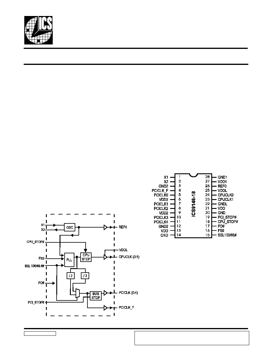
Block Diagram
Pentium/Pro
TM
System Clock Chip
9148-18 Rev B 07/08/98
Pin Configuration
28 pin SSOP
Pentium is a trademark on Intel Corporation.
Generates system clocks for CPU, PCI,
plus 14.314 MHz REF0.
Supports single or dual processor systems
Skew from CPU (earlier) to PCI clock (rising edges for
100/33.3MHz) 1 to 4ns
Separate 2.5V and 3.3V supply pins
2.5V or 3.3V output: CPU
3.3V outputs: PCI, REF
No power supply sequence requirements
Uses external 14.318MHz crystal, no external load cap
required for C
L
=18pF crystal
28 pin 209 mil SSOP
The ICS9148-18 is a Clock Synthesizer chip for Pentium and
PentiumPro CPU based Desktop/Notebook systems that will
provide all necessary clock timing.
Features include two CPU and six PCI clocks. One reference
output is available equal to the crystal frequency. Additionally,
the device meets the Pentium power-up stabilization
requirement, acheiving stable CPU and PCI clocks 2ms after
power-up.
PD# pin can enable a low power mode by stopping crystal
OSC and PLL stages. Other power management features
include, CPU_STOP# which stops CPU (0:1) clocks, and
PCI_STOP# which stops PCICLK (0:4) clocks.
High drive CPUCLK outputs typically provide greater than 1
V/ns slew rate into 20pF loads. PCICLK outputs typically
provide better than 1V/ns slew rate into 30pF loads while
maintaining 50±5% duty cycle. The REF clock output typically
provides better than 0.5V/ns slew rates.
The ICS9148-18 accepts a 14.318MHz reference crystal or
clock as its input and runs on a 3.3V core supply.
Ground Groups
GND = Ground Source Core
GND1 = REF0, X1, X2
GND2 = PCICLK_F, PCICLK (0:4)
GNDL = CPUCLK (0:1)
Power Groups
VDD = Supply for PLL core
VDD1 = REF0, X1, X2
VDD2 = PCICLK_F, PCICLK (0:4)
VDDL = CPUCLK (0:1)
ICS reserves the right to make changes in the device data identified in this
publication without further notice. ICS advises its customers to obtain the latest
version of all device data to verify that any information being relied upon by the
customer is current and accurate.
2
ICS9148-18
Pin Descriptions
Select Functions
(Functionality determined by FS0 and SEL100/66# pin, see below)
Notes:
1. TCLK is a test clock driven on the X1 (crystal in pin) input during test mode.
PIN NUMBER
PIN NAME
TYPE
DESCRIPTION
26
REF0
OUT
14.318MHz clock output
28
GND1
PWR
Ground for REF outputs
1
X1
IN
XTAL_IN 14.318MHz Crystal input, has internal 33pF load
cap and feed back resistor from X2
2
X2
OUT
XTAL_OUT Crystal output, has internal load cap 33pF
3, 12
GND2
PWR
Ground for PCI outputs
4
PCICLK_F
OUT
Free Running PCI output
5, 7, 8, 10, 11
PCICLK (0:4)
OUT
PCI clock outputs. TTL compatible 3.3V
6, 9
VDD2
PWR
Power for PCICLK outputs, nominally 3.3V
13, 21
VDD
PWR
Isolated power for core, nominally 3.3V
14, 20
GND
PWR
Isolated ground for core
15
SEL100/66.6#
IN
Select pin for enabling 100MHz or 66.6MHz
H=100MHz, L=66.6MHz (PCI always synchronous 33.3MHz)
16
FS0
IN
Frequency Select pin
17
PD#
IN
Powers down chip, active low
18
CPU_STOP#
IN
Halts CPU clocks at logic "0" level when low
19
PCI_STOP#
IN
Halts PCI Bus at logic "0" level when low
25
VDDL
PWR
Power for CPU outputs, nominally 2.5V
22
GNDL
PWR
Ground for CPU outputs.
23, 24
CPUCLK (1:0)
OUT
CPU and Host clock outputs @ 2.5V
27
VDD1
PWR
Power for REF outputs.
Functionality
CPUCLK
PCI,
PCI_F
REF0
Tristate
HI - Z
HI - Z
HI - Z
Testmode
TCLK/2
1
TCLK/6
1
TCLK
1
SEL 100/66#
FS0
Function
0
0
Tri-State
0
-
(Reserved)
0
-
(Reserved)
0
1
Active 66.6MHz CPU, 33.3 PCI
1
0
Test Mode
1
-
(Reserved)
1
-
(Reserved)
1
1
Active 100MHz CPU, 33.3 PCI

3
ICS9148-18
Technical Pin Function Descriptions
VDD(1,2)
This is the power supply to the internal core logic of the
device as well as the clock output buffers for REF0, PCICLK
(0:4), and PCICLK_F.
This pin operates at 3.3V volts. Clocks from the buffers that
it supplies will have a voltage swing from Ground to this
level. For the actual guaranteed high and low voltage levels
for the clocks, please consult the DC parameter table in this
data sheet.
VDDL
This is the power supply for the CPUCLK output buffers.
The voltage level for these outputs may be 2.5 or 3.3volts.
Clocks from the buffers that this pin supplies will have a
voltage swing from Ground to VDDL. For the actual
guaranteed high and low voltage levels of these Clocks,
please consult the DC parameter table in this data sheet.
GND(1,2)
This is the power supply ground (common or negative) return
pin for the internal core logic and all the PCI output buffers.
GNDL
This is the ground for CPUCLK output buffers.
X1
This input pin serves one of two functions. When the device
is used with a crystal, X1 acts as the input pin for the
reference signal that comes from the crystal. When the device
is driven by an external clock signal, X1 is the device input
pin for that reference clock. This pin also has an internal
Crystal loading capacitor that is connected to ground. With
a nominal value of 33pF, no external load cap is needed for a
C
L
=17 to 18pF crystal.
X2
This Output pin is used only when the device uses a crystal
as the reference frequency source. In this mode of operation,
X2 is an output signal that drives (or excites) the crystal. The
X2 pin also has an internal loading capacitor, nominally 33pF.
CPUCLK (0:1)
These output pins are the clock outputs that drive processor
and other CPU related circuitry that requires clocks which
are in tight skew tolerance with the CPU clock. The voltage
swing of these clocks is controlled by the voltage level
applied to the VDDL pin of the device. See the Functionality
Table for a list of the specific frequencies that are available
for these clocks and the selection codes to produce them.
REF0
The REF Output is fixed frequency clock that runs at the
same frequency as the Input Reference Clock or the Crystal
(typically 14.31818MHz) attached across X1 and X2.
PCICLK_F
This Output is equal to PCICLK(0:4) and is FREE RUNNING,
and will not be stopped by PCI_STOP#.
PCICLK (0:4)
These output clocks generate all the PCI timing requirements
for a Pentium/Pro based system. They conform to the
current PCI specification.
SELECT 100/66.6MHz#
This input pin controls the frequency of the clocks at the
CPU & PCICLK output pins. If a logic 1 value is present on
this pin, the 100MHz clock is selected. If a logic 0 is used,
the 66.6MHz frequency is selected. The PCI clock is
multiplexed to run at 33.3MHz for both select cases. PCI is
synchronous at the rising edge of PCI to the CPU rising edge
(with the skew making CPU early).
PD#
This is an asynchronous active low input pin used to power
down the device into a low power state. The internal clocks
are disabled and the VCO and Crystal are stopped. Power
down will also place all the outputs in a low state at the end of
their current cycle. The latency of power down will not be
greater than 3ms.
CPU_STOP#
This is a synchronous active low input pin used to stop the
CPUCLK clocks in an active low state. All other clocks will
continue to run while this function is enabled. The CPUCLKs
will have a turn ON latency of at least 3 CPU clocks.
PCI_STOP#
This is a synchronous active low input pin used to stop the
PCICLK clocks in an active low state. It will not effect
PCICLK_F nor any other outputs.
4
ICS9148-18
Power Management
ICS9148-18 Power Management Requirements
Clock Enable Configuration
Full clock cycle timing is guaranteed at all times after the system has initially powered up except where noted. During power
up and power down operations using the PD# pin will not cause clocks of a short or longer pulse than that of the running clock.
The first clock pulse coming out of a stopped clock condition may be slightly distorted due to clock network charging circuitry.
Board routing and signal loading may have a large impact on the initial clock distortion also.
Notes.
1. Clock on latency is defined from when the clock enable goes active to when the first valid clock comes out of the device.
2. Clock off latency is defined from when the clock enable goes inactive to when the last clock is driven low out of the device.
3. Power up latency is when PD# goes inactive (high) to when the first valid clocks are output by the device.
4. Power down has controlled clock counts applicable to CPUCLK, PCICLK only.
The REF and IOAPIC will be stopped independant of these.
SIGNAL
SIGNAL STATE
Latency
No. of rising edges of free
running PCICLK
CPU_ STOP#
0 (Disabled)
2
1
1 (Enabled)
1
1
PCI_STOP#
0 (Disabled)
2
1
1 (Enabled)
1
1
PD#
1 (Normal Operation)
3
3ms
0 (Power Down)
4
2max
CPU_STOP#
PCI_STOP#
PWR_DWN#
CPUCLK
PCICLK
REF
Crystal
VCOs
X
X
0
Low
Low
Stopped
Off
Off
0
0
1
Low
Low
Running
Running
Running
0
1
1
Low
33.3 MHz
Running
Running
Running
1
0
1
100/66.6MHz
Low
Running
Running
Running
1
1
1
100/66.6MHz
33.3 MHz
Running
Running
Running
5
ICS9148-18
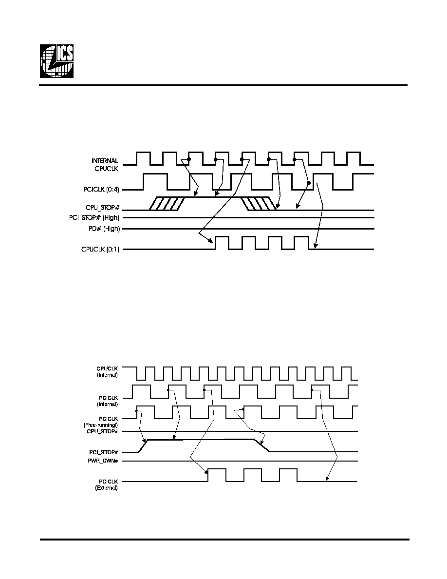
PCI_STOP# Timing Diagram
PCI_STOP# is an asynchronous input to the ICS9148-18. It is used to turn off the PCICLK (0:4) clocks for low power operation.
PCI_STOP# is synchronized by the ICS9148-18 internally. The minimum that the PCICLK (0:4) clocks are enabled (PCI_STOP#
high pulse) is at least 10 PCICLK (0:4) clocks. PCICLK (0:4) clocks are stopped in a low state and started with a full high pulse
width guaranteed. PCICLK (0:4) clock on latency cycles are only one rising PCICLK clock off latency is one PCICLK clock.
CPU_STOP# Timing Diagram
CPUSTOP# is an asychronous input to the clock synthesizer. It is used to turn off the CPUCLKs for low power operation.
CPU_STOP# is synchronized by the ICS9148-18. The minimum that the CPUCLK is enabled (CPU_STOP# high pulse) is 100
CPUCLKs. All other clocks will continue to run while the CPUCLKs are disabled. The CPUCLKs will always be stopped in a low
state and start in such a manner that guarantees the high pulse width is a full pulse. CPUCLK on latency is less than 4 CPUCLKs
and CPUCLK off latency is less than 4 CPUCLKs.
Notes:
1. All timing is referenced to the internal CPUCLK.
2. CPU_STOP# is an asynchronous input and metastable conditions may exist.
This signal is synchronized to the CPUCLKs inside the ICS9148-18.
3. All other clocks continue to run undisturbed.
4. PD# and PCI_STOP# are shown in a high (true) state.
Notes:
1. All timing is referenced to the Internal CPUCLK (defined as inside the ICS9148 device.)
2. PCI_STOP# is an asynchronous input, and metastable conditions may exist. This signal is required to be synchronized
inside the ICS9148.
3. All other clocks continue to run undisturbed.
4. PD# and CPU_STOP# are shown in a high (true) state.