Äîêóìåíòàöèÿ è îïèñàíèÿ www.docs.chipfind.ru
Integrated
Circuit
Systems, Inc.
General Description
Features
ICS9148-93
Advance Information
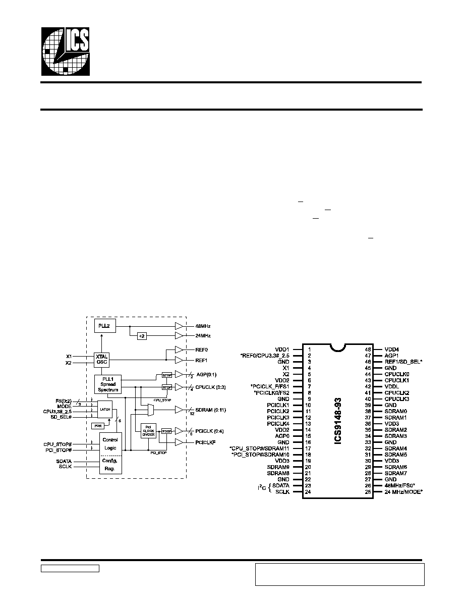
Block Diagram
Pentium is a trademark of Intel Corporation
I
2
C is a trademark of Philips Corporation
Frequency Generator & Integrated Buffers for PENTIUM/Pro
TM
9148-93 Rev - 1/22/99
Pin Configuration
Generates the following system clocks:
- 4 CPU(2.5V/3.3V) upto 100MHz.
- 6 PCI(3.3V) @ 33.3MHz
- 2AGP(3.3V) @ 2 x PCI
- 12 SDRAMs(3.3V) @ either CPU or AGP
- 2 REF (3.3V) @ 14.318MHz
Skew characteristics:
- CPU CPU<250ps
- SDRAM SDRAM < 250ps
- CPU SDRAM < 250ps
- CPU(early) PCI : 1-4ns
Supports Spread Spectrum modulation +0.25, ±0.6%
Serial I
2
C interface for Power Management, Frequency
Select, Spread Spectrum.
Efficient Power management scheme through PCI and CPU
STOP CLOCKS.
Uses external 14.318MHz crystal
48 pin 300mil SSOP.
48-Pin SSOP
Power Groups
VDD1 = REF (0:1), X1, X2
VDD2 = PCICLK_F, PCICLK(0:5)
VDD3 = SDRAM (0:11), supply for PLL core,
24 MHz, 48MHz
VDD4 = AGP (0:1)
VDDL = CPUCLK (0:3)
* Internal Pull-up Resistor of
240K to 3.3V on indicated inputs
The ICS9148-93 is the single chip clock solution for Desktop/
Notebook designs using the VIA MVP3 style chipset. It
provides all necessary clock signals for such a system.
Spread spectrum may be enabled through I
2
C programming.
Spread spectrum typically reduces system EMI by 8dB to
10dB. This simplifies EMI qualification without resorting to
board design iterations or costly shielding. The ICS9148-93
employs a proprietary closed loop design, which tightly
controls the percentage of spreading over process and
temperature variations.
Serial programming I
2
C interface allows changing functions,
stop clock programming and frequency selection. The SD_SEL
latched input allows the SDRAM frequency to follow the
CPUCLK frequency(SD_SEL=1) or the AGP clock
frequency(SD_SEL=0).
ADVANCE INFORMATION documents contain information on products
in the formative or design phase development. Characteristic data and
other specifications are design goals. ICS reserves the right to change or
discontinue these products without notice.
2
ICS9148- 93
Advance Information
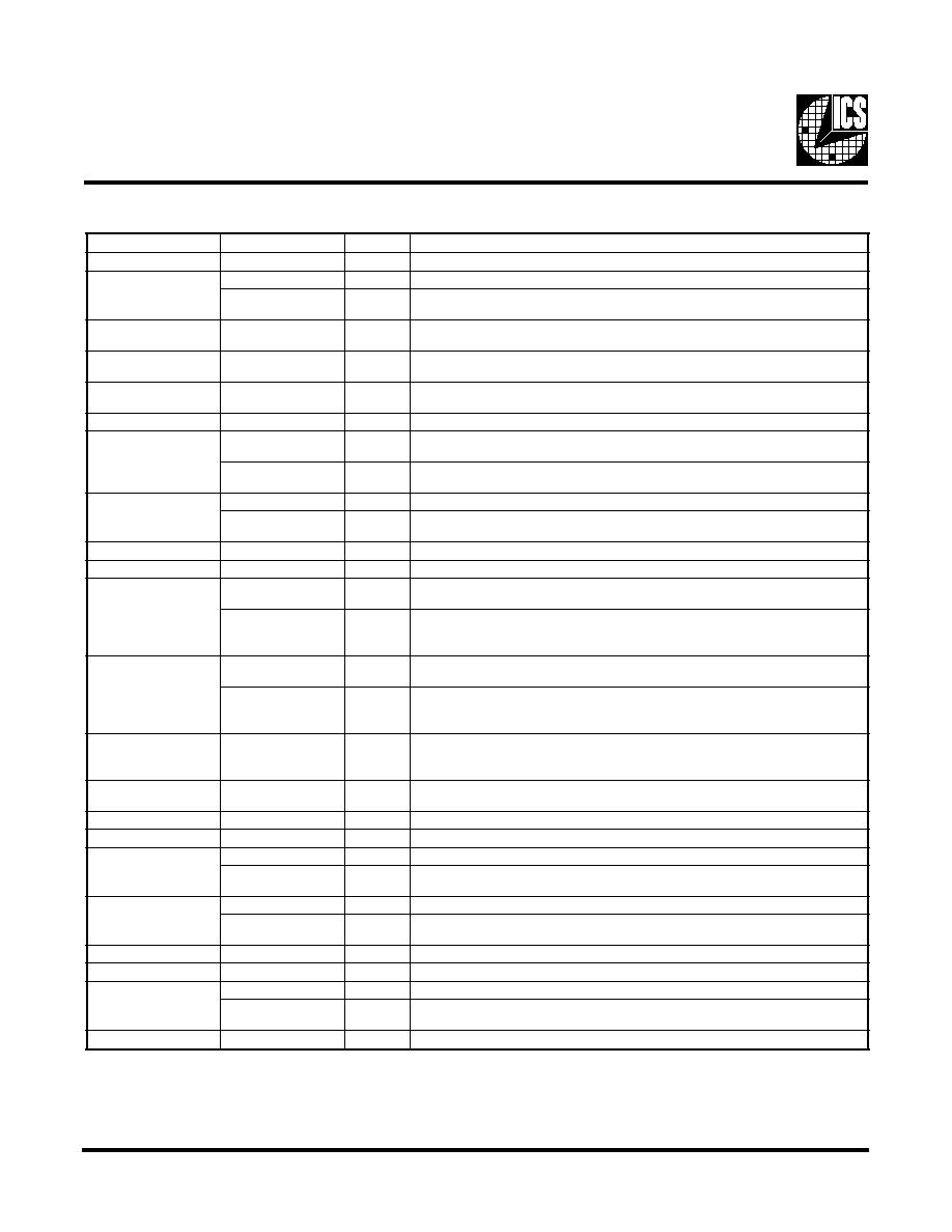
Pin Descriptions
Notes:
1:
Internal Pull-up Resistor of 240K to 3.3V on indicated inputs
2:
Bidirectional input/output pins, input logic levels are latched at internal power-on-reset. Use 10Kohm resistor to
program logic Hi to VDD or GND for logic low.
R
E
B
M
U
N
N
I
P
E
M
A
N
N
I
P
E
P
Y
T
N
O
I
T
P
I
R
C
S
E
D
1
1
D
D
V
R
W
P
V
3
.
3
l
a
n
i
m
o
n
,
y
l
p
p
u
s
r
e
w
o
p
L
A
T
X
,
)
2
:
0
(
f
e
R
2
0
F
E
R
T
U
O
.
k
c
o
l
c
e
c
n
e
r
e
f
e
r
z
H
M
8
1
3
.
4
1
5
.
2
_
#
3
.
3
U
P
C
2
,
1
N
I
V
3
.
3
=
W
O
L
,
U
P
C
V
5
.
2
=
h
g
i
H
.
V
5
.
2
r
o
V
3
.
3
s
i
2
L
D
D
V
r
e
h
t
e
h
w
s
e
t
a
c
i
d
n
I
U
P
C
1
t
u
p
n
i
d
e
h
c
t
a
L
.
2
,
7
2
,
2
2
,
6
1
,
9
,
3
5
4
,
9
3
,
3
3
D
N
G
R
W
P
d
n
u
o
r
G
4
1
X
N
I
k
c
a
b
d
e
e
f
d
n
a
)
F
p
3
3
(
p
a
c
d
a
o
l
l
a
n
r
e
t
n
i
s
a
h
,
t
u
p
n
i
l
a
t
s
y
r
C
2
X
m
o
r
f
r
o
t
s
i
s
e
r
5
2
X
T
U
O
d
a
o
l
l
a
n
r
e
t
n
i
s
a
H
.
z
H
M
8
1
3
.
4
1
y
l
l
a
n
i
m
o
n
,
t
u
p
t
u
o
l
a
t
s
y
r
C
)
F
p
3
3
(
p
a
c
4
1
,
6
2
D
D
V
R
W
P
V
3
.
3
l
a
n
i
m
o
n
,
)
5
:
0
(
K
L
C
I
C
P
d
n
a
F
_
K
L
C
I
C
P
r
o
f
y
l
p
p
u
S
7
F
_
K
L
C
I
C
P
T
U
O
w
e
k
s
s
n
4
-
1
h
t
i
w
s
K
L
C
U
P
C
h
t
i
w
s
u
o
n
o
r
h
c
n
y
S
.
t
u
p
t
u
o
k
c
o
l
c
I
C
P
g
n
i
n
n
u
r
e
e
r
F
#
P
O
T
S
_
I
C
P
y
b
d
e
t
c
e
f
f
a
t
o
n
s
i
s
i
h
T
)
y
l
r
a
e
U
P
C
(
1
S
F
2
,
1
N
I
e
h
t
s
e
n
i
m
r
e
t
e
d
s
n
i
p
S
F
r
e
h
t
o
h
t
i
w
g
n
o
l
A
.
t
u
p
n
I
d
e
h
c
t
a
L
.
n
i
p
t
c
e
l
e
s
y
c
n
e
u
q
e
r
F
.
s
e
i
c
n
e
u
q
e
r
f
P
G
A
&
I
C
P
,
M
A
R
D
S
,
U
P
C
8
0
K
L
C
I
C
P
T
U
O
)
y
l
r
a
e
U
P
C
(
w
e
k
s
s
n
4
-
1
h
t
i
w
s
K
L
C
U
P
C
s
u
o
n
o
r
h
c
n
y
S
.
t
u
p
t
u
o
k
c
o
l
c
I
C
P
2
S
F
2
,
1
N
I
e
h
t
s
e
n
i
m
r
e
t
e
d
s
n
i
p
S
F
r
e
h
t
o
h
t
i
w
g
n
o
l
A
t
u
p
n
I
d
e
h
c
t
a
L
.
n
i
p
t
c
e
l
e
s
y
c
n
e
u
q
e
r
F
.
s
e
i
c
n
e
u
q
e
r
f
P
G
A
&
I
C
P
,
M
A
R
D
S
,
U
P
C
3
1
,
2
1
,
1
1
,
0
1
)
4
:
1
(
K
L
C
I
C
P
T
U
O
)
y
l
r
a
e
U
P
C
(
w
e
k
s
s
n
4
-
1
h
t
i
w
s
K
L
C
U
P
C
s
u
o
n
o
r
h
c
n
y
S
.
s
t
u
p
t
u
o
k
c
o
l
c
I
C
P
7
4
,
5
1
)
1
:
0
(
P
G
A
T
U
O
.
4
D
D
V
y
b
d
e
r
e
w
o
p
,
s
t
u
p
t
u
o
t
r
o
P
c
i
h
p
a
r
G
d
e
c
n
a
v
d
A
7
1
#
P
O
T
S
_
U
P
C
1
N
I
0
c
i
g
o
l
t
a
s
k
c
o
l
c
)
1
:
0
(
P
G
A
d
n
a
)
3
:
0
(
K
L
C
U
P
C
s
t
l
a
h
t
u
p
n
i
s
u
o
n
o
r
h
c
n
y
s
a
s
i
h
T
)
0
=
E
D
O
M
,
e
d
o
M
e
l
i
b
o
M
n
i
(
w
o
l
t
u
p
n
i
n
e
h
w
,
l
e
v
e
l
1
1
M
A
R
D
S
T
U
O
.
t
u
p
n
i
d
e
h
c
t
a
l
L
E
S
_
D
S
e
h
t
y
b
d
e
t
c
e
l
e
s
s
i
y
c
n
e
u
q
e
r
F
.
t
u
p
t
u
o
k
c
o
l
c
M
A
R
D
S
y
c
n
e
u
q
e
r
f
U
P
C
=
y
c
n
e
u
q
e
r
f
M
A
R
D
S
s
e
s
u
a
c
n
o
r
e
w
o
p
t
a
1
=
L
E
S
_
D
S
y
c
n
e
u
q
e
r
f
P
G
A
=
y
c
n
e
u
q
e
r
f
M
A
R
D
S
s
e
s
u
a
c
n
o
r
e
w
o
p
t
a
0
=
L
E
S
_
D
S
8
1
#
P
O
T
S
_
I
C
P
1
N
I
n
e
h
w
,
l
e
v
e
l
0
c
i
g
o
l
t
a
s
k
c
o
l
c
)
5
:
0
(
K
L
C
I
C
P
s
t
l
a
h
t
u
p
n
i
s
u
o
n
o
r
h
c
n
y
s
a
s
i
h
T
)
0
=
E
D
O
M
,
e
d
o
m
e
l
i
b
o
m
n
I
(
w
o
l
t
u
p
n
i
0
1
M
A
R
D
S
T
U
O
.
t
u
p
n
i
d
e
h
c
t
a
l
L
E
S
_
D
S
e
h
t
y
b
d
e
t
c
e
l
e
s
s
i
y
c
n
e
u
q
e
r
F
.
t
u
p
t
u
o
k
c
o
l
c
M
A
R
D
S
y
c
n
e
u
q
n
e
r
f
U
P
C
=
y
c
n
e
u
q
e
r
f
M
A
R
D
S
s
e
s
u
a
c
n
o
r
e
w
o
p
t
a
1
=
L
E
S
_
D
S
y
c
n
e
u
q
e
r
f
P
G
A
=
y
c
n
e
u
q
e
r
f
M
A
R
D
S
s
e
s
u
a
c
n
o
r
e
w
o
p
t
a
0
=
L
E
S
_
D
S
,
1
3
,
9
2
,
8
2
,
1
2
,
0
2
8
3
,
7
3
,
5
3
,
4
3
,
2
3
)
9
:
0
(
M
A
R
D
S
T
U
O
.
t
u
p
n
i
d
e
h
c
t
a
l
L
E
S
_
D
S
e
h
t
y
b
d
e
t
c
e
l
e
s
s
i
y
c
n
e
u
q
e
r
F
.
s
t
u
p
t
u
o
k
c
o
l
c
M
A
R
D
S
y
c
n
e
u
q
e
r
f
U
P
C
=
y
c
n
e
u
q
e
r
f
M
A
R
D
S
s
e
s
u
a
c
n
o
r
e
w
o
p
t
a
1
=
L
E
S
_
D
S
y
c
n
e
u
q
e
r
f
P
G
A
=
s
e
i
c
n
e
u
q
e
r
f
M
A
R
D
S
s
e
s
u
a
c
n
o
r
e
w
o
p
t
a
0
=
L
E
S
_
D
S
6
3
,
0
3
,
9
1
3
D
D
V
R
W
P
,
s
k
c
o
l
c
z
H
M
8
4
,
4
2
d
n
a
e
r
o
C
U
P
C
,
)
1
1
:
0
(
M
A
R
D
S
r
o
f
y
l
p
p
u
S
.
V
3
.
3
l
a
n
i
m
o
n
3
2
A
T
A
D
S
N
I
I
r
o
f
t
u
p
n
i
a
t
a
D
2
.
t
u
p
n
i
l
a
i
r
e
s
C
4
2
K
L
C
S
N
I
I
f
o
t
u
p
n
i
k
c
o
l
C
2
t
u
p
n
i
C
5
2
z
H
M
4
2
T
U
O
.
g
n
i
m
i
t
O
/
I
r
e
p
u
S
r
o
f
,
k
c
o
l
c
t
u
p
t
u
o
z
H
M
4
2
E
D
O
M
2
,
1
N
I
.
e
d
o
M
e
l
i
b
o
M
=
0
,
e
d
o
M
p
o
t
k
s
e
D
=
1
,
n
i
p
t
c
e
l
e
s
n
o
i
t
c
n
u
f
8
1
n
i
p
,
7
1
n
i
P
.
t
u
p
n
I
d
e
h
c
t
a
L
6
2
z
H
M
8
4
T
U
O
.
g
n
i
m
i
t
B
S
U
r
o
f
,
k
c
o
l
c
t
u
p
t
u
o
z
H
M
8
4
0
S
F
2
,
1
N
I
e
h
t
s
e
n
i
m
r
e
t
e
d
s
n
i
p
S
F
r
e
h
t
o
h
t
i
w
g
n
o
l
A
t
u
p
n
I
d
e
h
c
t
a
L
.
n
i
p
t
c
e
l
e
s
y
c
n
e
u
q
e
r
F
.
s
e
i
c
n
e
u
q
e
r
f
P
G
A
&
I
C
P
,
M
A
R
D
S
,
U
P
C
4
4
,
3
4
,
1
4
,
0
4
)
3
:
0
(
K
L
C
U
P
C
T
U
O
w
o
L
=
#
P
O
T
S
_
U
P
C
f
i
w
o
L
.
2
L
D
D
V
y
b
d
e
r
e
w
o
p
,
s
t
u
p
t
u
o
k
c
o
l
c
U
P
C
2
4
L
D
D
V
R
W
P
l
a
n
i
m
o
n
V
3
.
3
r
o
V
5
.
2
r
e
h
t
i
e
,
)
3
:
0
(
U
P
C
r
o
f
y
l
p
p
u
S
6
4
1
F
E
R
T
U
O
.
k
c
o
l
c
e
c
n
e
r
e
f
e
r
z
H
M
8
1
3
.
4
1
L
E
S
_
D
S
N
I
P
G
A
r
o
)
1
=
L
E
S
D
S
(
U
P
C
r
e
h
t
i
e
s
t
c
e
l
e
s
n
O
r
e
w
o
P
t
a
t
u
p
n
i
d
e
h
c
t
a
L
.
s
t
u
p
t
u
o
k
c
o
l
c
M
A
R
D
S
e
h
t
r
o
f
s
e
i
c
n
e
u
q
e
r
f
)
0
=
L
E
S
_
D
S
(
8
4
4
D
D
V
R
W
P
)
1
:
0
(
P
G
A
r
o
f
y
l
p
p
u
S
3
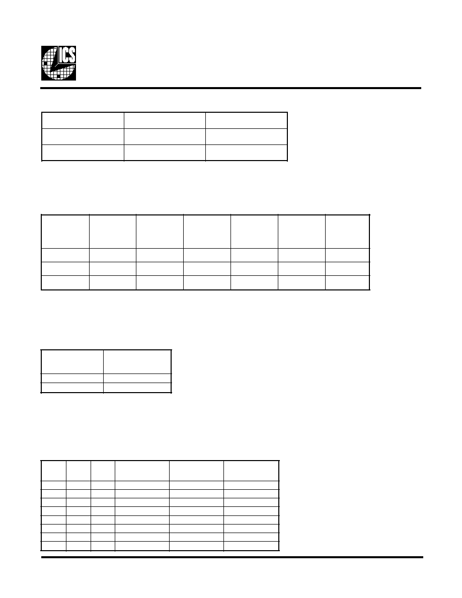
ICS9148-93
Advance Information
Functionality
V
DD
1, 2, 3, 4 = 3.3V±5%, V
DDL
= 2.5V ±5% or 3.3 ±5%, TA= 0 to 70°C
Crystal (X1, X2) = 14.31818MHz
5
.
2
_
#
3
.
3
U
P
C
l
e
v
e
l
t
u
p
n
I
)
a
t
a
D
d
e
h
c
t
a
L
(
r
o
f
d
e
t
c
e
l
e
S
r
e
f
f
u
B
:
t
a
n
o
i
t
a
r
e
p
o
1
D
D
V
V
5
.
2
0
D
D
V
V
3
.
3
CPU 3.3#_2.5V Buffer selector for CPUCLK drivers.
Power Management Functionality
Mode Pin - Power Management Input Control
5
2
n
i
P
,
E
D
O
M
)
t
u
p
n
I
d
e
h
c
t
a
L
(
7
1
n
i
P
8
1
n
i
P
0
#
P
O
T
S
_
U
P
C
)
T
U
P
N
I
(
#
P
O
T
S
_
I
C
P
)
T
U
P
N
I
(
1
1
1
M
A
R
D
S
)
T
U
P
T
U
O
(
0
1
M
A
R
D
S
)
T
U
P
T
U
O
(
#
P
O
T
S
_
U
P
C
#
P
O
T
S
_
I
C
P
,
P
G
A
K
L
C
U
P
C
s
t
u
p
t
u
O
K
L
C
I
C
P
)
5
:
0
(
,
F
_
K
L
C
I
C
P
,
F
E
R
z
H
M
8
4
/
4
2
M
A
R
D
S
d
n
a
l
a
t
s
y
r
C
C
S
O
O
C
V
0
1
w
o
L
d
e
p
p
o
t
S
g
n
i
n
n
u
R
g
n
i
n
n
u
R
g
n
i
n
n
u
R
g
n
i
n
n
u
R
1
1
g
n
i
n
n
u
R
g
n
i
n
n
u
R
g
n
i
n
n
u
R
g
n
i
n
n
u
R
g
n
i
n
n
u
R
1
0
g
n
i
n
n
u
R
w
o
L
d
e
p
p
o
t
S
g
n
i
n
n
u
R
g
n
i
n
n
u
R
g
n
i
n
n
u
R
2
S
F
1
S
F
0
S
F
)
z
H
M
(
U
P
C
)
z
H
M
(
M
A
R
D
S
)
z
H
M
(
I
C
P
)
z
H
M
(
P
G
A
0
0
0
0
0
.
0
9
0
0
.
0
3
0
0
.
0
6
0
0
1
2
8
.
6
6
1
4
.
3
3
2
8
.
6
6
0
1
0
9
4
.
8
6
5
2
.
4
3
9
4
.
8
6
0
1
1
0
0
.
5
7
5
.
7
3
0
0
.
5
7
1
0
0
0
0
.
5
7
0
0
.
0
3
0
0
.
0
6
1
0
1
1
3
.
3
8
2
3
.
3
3
4
6
.
6
6
1
1
0
5
2
.
5
9
5
7
.
1
3
0
5
.
3
6
1
1
1
0
0
.
0
0
1
3
3
.
3
3
6
6
.
6
6
4
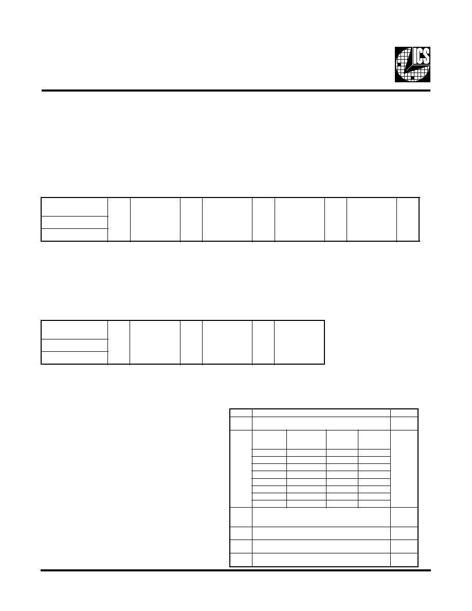
ICS9148- 93
Advance Information
Byte0: Functionality and Frequency Select Register
(default = 0)
Serial Configuration Command Bitmap
General I
2
C serial interface information
The information in this section assumes familiarity with I
2
C programming. For more information, contact ICS for an I
2
C
programming application note.
How to Write:
Send the address D2
(H)
.
Send two additional dummy bytes, a command code
and byte count.
Send the desired number of data bytes.
See the diagram below:
Note that the acknowledge bit is sent by the clock chip, and pulls the data line low. There is no minimum of data bytes that must
be sent.
How to Read:
Send the address D3
(H)
.
Send the byte count in binary coded decimal
Read back the desired number of data bytes
See the diagram below:
The following specifications should be observed:
1.
Operating voltage for I
2
C pins is 3.3V
2.
Maximum data transfer rate (SCLK) is 100K bits/sec.
r
o
t
a
r
e
n
e
G
k
c
o
l
C
)
s
t
i
b
7
(
s
s
e
r
d
d
A
K
C
A
s
t
i
b
8
+
y
m
m
u
d
e
d
o
c
d
n
a
m
m
o
c
K
C
A
s
t
i
b
8
+
e
t
y
B
y
m
m
u
d
t
n
u
o
c
K
C
A
e
t
y
B
a
t
a
D
1
K
C
A
e
t
y
B
a
t
a
D
N
K
C
A
#
W
/
R
&
)
0
:
6
(
A
2
D
)
H
(
r
o
t
a
r
e
n
e
G
k
c
o
l
C
)
s
t
i
b
7
(
s
s
e
r
d
d
A
K
C
A
e
t
y
B
t
n
u
o
C
K
C
A
e
t
y
B
a
t
a
D
1
K
C
A
e
t
y
B
a
t
a
D
N
#
W
/
R
&
)
0
:
6
(
A
3
D
)
H
(
I
2
C is a trademark of Philips Corporation
Note 1. Default at Power-up will be for latched logic inputs,
as defined by Bit 3.
t
i
B
n
o
i
t
p
i
r
c
s
e
D
D
W
P
7
t
i
B
n
o
i
t
a
l
u
d
o
M
m
u
r
t
c
e
p
S
d
a
e
r
p
S
%
5
2
.
0
±
-
0
n
o
i
t
a
l
u
d
o
M
m
u
r
t
c
e
p
S
d
a
e
r
p
S
%
6
.
0
±
-
1
0
t
i
B
4
:
6
)
4
:
6
(
t
i
B
U
P
C
M
A
R
D
S
)
z
H
M
(
I
C
P
)
z
H
M
(
P
G
A
)
z
H
M
(
X
X
X
1
e
t
o
N
0
0
0
0
0
.
0
9
0
0
.
0
3
0
0
.
0
6
1
0
0
2
8
.
6
6
1
4
.
3
3
2
8
.
6
6
0
1
0
9
4
.
8
6
5
2
.
4
3
9
4
.
8
6
1
1
0
0
0
.
5
7
0
5
.
7
3
0
0
.
5
7
0
0
1
0
0
.
5
7
0
0
.
0
3
0
0
.
0
6
1
0
1
1
3
.
3
8
2
3
.
3
3
4
6
.
6
6
0
1
1
5
2
.
5
9
5
7
.
1
3
0
5
.
3
6
1
1
1
0
0
.
0
0
1
3
3
.
3
3
6
6
.
6
6
3
t
i
B
,
t
c
e
l
e
s
e
r
a
w
d
r
a
h
y
b
d
e
t
c
e
l
e
s
s
i
y
c
n
e
u
q
e
r
F
-
0
y
l
n
o
s
n
i
p
)
2
:
0
(
S
F
I
y
b
s
e
i
c
n
e
u
q
e
r
f
t
c
e
l
e
S
-
1
2
C
0
d
a
e
r
p
S
r
e
t
n
e
C
-
0
d
a
e
r
p
S
n
w
o
D
-
1
0
1
t
i
B
n
o
i
t
a
r
e
p
o
l
a
m
r
o
N
-
0
d
e
l
b
a
n
E
m
u
r
t
c
e
p
S
d
a
e
r
p
S
-
1
0
0
t
i
B
g
n
i
n
n
u
R
-
0
s
t
u
p
t
u
o
l
l
a
e
t
a
t
s
i
r
T
-
1
0
5
ICS9148-93
Advance Information
Byte 1: CPU, Active/Inactive Register
(1 = enable, 0 = disable)
Byte 2: PCI Active/Inactive Register
(1 = enable, 0 = disable)
Byte 3: SDRAM Active/Inactive Register
(1 = enable, 0 = disable)
Notes:
1. Inactive means outputs are held LOW and are disabled
from switching.
Notes:
1. Inactive means outputs are held LOW and are disabled
from switching.
Notes:
1. Inactive means outputs are held LOW and are disabled
from switching.
t
i
B
#
n
i
P
D
W
P
n
o
i
t
p
i
r
c
s
e
D
7
t
i
B
-
1
)
d
e
v
r
e
s
e
R
(
6
t
i
B
-
1
)
d
e
v
r
e
s
e
R
(
5
t
i
B
-
1
)
d
e
v
r
e
s
e
R
(
4
t
i
B
-
1
)
d
e
v
r
e
s
e
R
(
3
t
i
B
0
4
1
)
t
c
a
n
I
/
t
c
A
(
3
K
L
C
U
P
C
2
t
i
B
1
4
1
)
t
c
a
n
I
/
t
c
A
(
2
K
L
C
U
P
C
1
t
i
B
3
4
1
)
t
c
a
n
I
/
t
c
A
(
1
K
L
C
U
P
C
0
t
i
B
4
4
1
)
t
c
a
n
I
/
t
c
A
(
0
K
L
C
U
P
C
t
i
B
#
n
i
P
D
W
P
n
o
i
t
p
i
r
c
s
e
D
7
t
i
B
-
1
)
d
e
v
r
e
s
e
R
(
6
t
i
B
7
1
)
t
c
a
n
I
/
t
c
A
(
F
_
K
L
C
I
C
P
5
t
i
B
5
1
1
)
t
c
a
n
I
/
t
c
A
(
0
P
G
A
4
t
i
B
3
1
1
)
t
c
a
n
I
/
t
c
A
(
4
K
L
C
I
C
P
3
t
i
B
2
1
1
)
t
c
a
n
I
/
t
c
A
(
3
K
L
C
I
C
P
2
t
i
B
1
1
1
)
t
c
a
n
I
/
t
c
A
(
2
K
L
C
I
C
P
1
t
i
B
0
1
1
)
t
c
a
n
I
/
t
c
A
(
1
K
L
C
I
C
P
0
t
i
B
8
1
)
t
c
a
n
I
/
t
c
A
(
0
K
L
C
I
C
P
t
i
B
#
n
i
P
D
W
P
n
o
i
t
p
i
r
c
s
e
D
7
t
i
B
8
2
1
)
t
c
a
n
I
/
t
c
A
(
7
M
A
R
D
S
6
t
i
B
9
2
1
)
t
c
a
n
I
/
t
c
A
(
6
M
A
R
D
S
5
t
i
B
1
3
1
)
t
c
a
n
I
/
t
c
A
(
5
M
A
R
D
S
4
t
i
B
2
3
1
)
t
c
a
n
I
/
t
c
A
(
4
M
A
R
D
S
3
t
i
B
4
3
1
)
t
c
a
n
I
/
t
c
A
(
3
M
A
R
D
S
2
t
i
B
5
3
1
)
t
c
a
n
I
/
t
c
A
(
2
M
A
R
D
S
1
t
i
B
7
3
1
)
t
c
a
n
I
/
t
c
A
(
1
M
A
R
D
S
0
t
i
B
8
3
1
)
t
c
a
n
I
/
t
c
A
(
0
M
A
R
D
S
Byte 4: SDRAM Active/Inactive Register
(1 = enable, 0 = disable)
Byte 5: Peripheral Active/Inactive Register
(1 = enable, 0 = disable)
Notes:
1. Inactive means outputs are held LOW and are disabled
from switching.
Notes:
1. Inactive means outputs are held LOW and are disabled
from switching.
t
i
B
#
n
i
P
D
W
P
n
o
i
t
p
i
r
c
s
e
D
7
t
i
B
-
1
)
d
e
v
r
e
s
e
R
(
6
t
i
B
-
1
)
d
e
v
r
e
s
e
R
(
5
t
i
B
-
1
)
d
e
v
r
e
s
e
R
(
4
t
i
B
-
1
)
d
e
v
r
e
s
e
R
(
3
t
i
B
7
1
1
)
t
c
a
n
I
/
t
c
A
(
1
1
M
A
R
D
S
)
y
l
n
O
e
d
o
M
p
o
t
k
s
e
D
(
2
t
i
B
8
1
1
)
t
c
a
n
I
/
t
c
A
(
0
1
M
A
R
D
S
)
y
l
n
O
e
d
o
M
p
o
t
k
s
e
D
(
1
t
i
B
0
2
1
)
t
c
a
n
I
/
t
c
A
(
9
M
A
R
D
S
0
t
i
B
1
2
1
)
t
c
a
n
I
/
t
c
A
(
8
M
A
R
D
S
t
i
B
#
n
i
P
D
W
P
n
o
i
t
p
i
r
c
s
e
D
7
t
i
B
-
1
)
d
e
v
r
e
s
e
R
(
6
t
i
B
-
1
)
d
e
v
r
e
s
e
R
(
5
t
i
B
-
1
)
d
e
v
r
e
s
e
R
(
4
t
i
B
7
4
1
)
t
c
a
n
I
/
t
c
A
(
1
P
G
A
3
t
i
B
-
1
)
d
e
v
r
e
s
e
R
(
2
t
i
B
-
1
)
d
e
v
r
e
s
e
R
(
1
t
i
B
6
4
1
)
t
c
a
n
I
/
t
c
A
(
1
F
E
R
0
t
i
B
2
1
)
t
c
a
n
I
/
t
c
A
(
0
F
E
R