Integrated
Circuit
Systems, Inc.
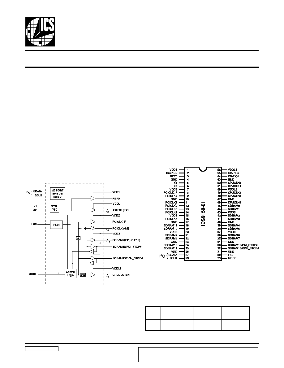
General Description
Features
ICS9150-01
Block Diagram
Pentium is a trademark of Intel Corporation
Pentium ProTM and SDRAM Frequency Generator
9150-01 RevE 4/25/01
Pin Configuration
The ICS9150-01 generates all clocks required for high speed
RISC or CISC microprocessor systems such as Intel
PentiumPro. Two different reference frequency multiplying
factors are externally selectable with smooth frequency
transitions. An output enable is provided for testability.
High drive PCICLK and SDRAM outputs typically provide
greater than 1 V/ns slew rate into 30 pF loads. CPUCLK
outputs typically provide better than 1V/ns slew rate into
20 pF loads while maintaining 50
±
5% duty cycle. The REF
clock outputs typically provide better than 0.5V/ns slew rates.
·
Generates five processor, six bus, one 14.31818MHz
and 16 SDRAM clocks.
·
Synchronous clocks skew matched to 250 ps window
on PCLKs and 500ps window on BCLKs
·
Test clock mode eases system design
·
Selectable multiplying ratios
·
Custom configurations available
·
Output frequency ranges to 100 MHz (depending on
option)
·
3.0V 3.7V supply range
·
PC serial configuration interface
·
Power Management Control Input pins
·
56-pin SSOP package
56-Pin SSOP
Functionality
0
S
F
,
K
L
C
U
P
C
M
A
R
D
S
)
z
H
M
(
F
E
R
,
1
X
)
z
H
M
(
K
L
C
I
C
P
)
z
H
M
(
0
0
.
0
6
8
1
3
.
4
1
0
3
1
6
.
6
6
8
1
3
.
4
1
3
.
3
3
ICS reserves the right to make changes in the device data identified in this
publication without further notice. ICS advises its customers to obtain the latest
version of all device data to verify that any information being relied upon by the
customer is current and accurate.

4
ICS9150- 01
VDD(1,2,3)
This is the power supply to the internal core logic of the device as well
as the clock output buffers for REF(0:1), PCICLK, and
SDRAM(0:7).
This pin operates at 3.3V volts. Clocks from the listed buffers that it
supplies will have a voltage swing from Ground to this level. For the
actual guaranteed high and low voltage levels for the Clocks, please
consult the DC parameter table in this data sheet.
VDDL1,2
This is the power supplies for the CPUCLK and IOAPCI output
buffers. The voltage level for these outputs may be 2.5 or 3.3volts.
Clocks from the buffers that each supplies will have a voltage swing
from Ground to this level. For the actual Guaranteed high and low
voltage levels of these Clocks, please consult the DC parameter
table in this Data Sheet.
GND
This is the power supply ground (common or negative) return pin for
the internal core logic and all the output buffers.
X1
This input pin serves one of two functions. When the device is used
with a Crystal, X1 acts as the input pin for the reference signal that
comes from the discrete crystal. When the device is driven by an
external clock signal, X1 is the device input pin for that reference
clock. This pin also implements an internal Crystal loading capacitor
that is connected to ground. See the data tables for the value of this
capacitor.
X2
This Output pin is used only when the device uses a Crystal as the
reference frequency source. In this mode of operation, X2 is an
output signal that drives (or excites) the discrete Crystal. The X2 pin
will also implement an internal Crystal loading capacitor that is
connected to ground. See the Data Sheet for the value of this
capacitor.
CPUCLK (0:4)
These Output pins are the Clock Outputs that drive processor and
other CPU related circuitry that requires clocks which are in tight
skew tolerance with the CPU clock. The voltage swing of these
Clocks are controlled by the Voltage level applied to the VDDL2 pin
of the device. See the Functionality Table for a list of the specific
frequencies that are available for these Clocks and the selection
codes to produce them.
SDRAM(0:15)
These Output Clocks are use to drive Dynamic RAM's and are low
skew copies of the CPU Clocks. The voltage swing of the
SDRAM's output is controlled by the supply voltage that is applied
to VDD3 of the device, operates at 3.3 volts.
IOAPIC (0:2)
These Outputs are fixed frequency Output Clocks that run at the
Reference Input (typically 14.31818MHz) . Its voltage level swing
is controlled by VDDL1 and may operate at 2.5 or 3.3volts.
Technical Pin Function Descriptions
REF0
The REF Output is a fixed frequency Clock that runs at the same
frequency as the Input Reference Clock X1 or the Crystal (typically
14.31818MHz) attached across X1 and X2.
PCICLK_F
This Output is equal to PCICLK(0:5) and is FREE RUNNING, and
will not be stopped by PCI_STP#.
PCICLK (0:5)
These Output Clocks generate all the PCI timing requirements for a
Pentium/Pro based system. They conform to the current PCI
specification. They run at 1/2 CPU frequency.
FS0
This Input pin controls the frequency of the Clocks at the CPU,
PCICLK and SDRAM output pins. If a logic "1" value is present on
this pin, the 66.6 MHz Clock will be selected. If a logic "0" is used,
the 60MHz frequency will be selected. (This is the Power Management
Mode)
MODE
This Input pin is used to select the Input function of the I/O pins.
An active Low will place the I/O pins in the Input mode and enable
those stop clock functions. (This is the Power Management Mode)
CPU_STOP#
This is a synchronous active Low Input pin used to stop the CPUCLK
clocks in an active low state. All other Clocks including SDRAM
clocks will continue to run while this function is enabled. The
CPUCLK's will have a turn ON latency of at least 3 CPU clocks. This
input pin only valid when MODE=0 (Power Management Mode)
PCI_STOP#
This is a synchronous active Low Input pin used to stop the PCICLK
clocks in an active low state. It will not effect PCICLK_F nor any
other outputs. This input pin only valid when MODE=0 (Power
Management Mode)
I
2
C
The SDATA and SCLOCK Inputs are use to program the device. The
clock generator is a slave-receiver device in the I
2
C protocol. It will
allow read-back of the registers. See configuration map for register
functions. The I
2
C specification in Philips I
2
C Peripherals Data
Handbook (1996) should be followed.
5
ICS9150-01
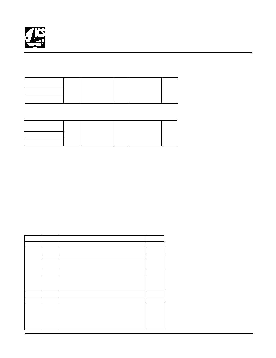
Serial Configuration Command Bitmaps
Byte 0: Functional and Frequency Select Clock Register (default = 0)
T
I
B
#
N
I
P
N
O
I
T
P
I
R
C
S
E
D
D
W
P
7
ti
B
-
d
e
v
r
e
s
e
R
0
6
ti
B
-
n
o
it
a
r
e
p
o
l
a
m
r
o
n
r
o
f
0
e
b
t
s
u
M
0
5
ti
B
-
n
o
it
a
r
e
p
o
l
a
m
r
o
n
r
o
f
0
e
b
t
s
u
M
0
-
e
p
y
t
s
l
o
r
t
n
o
C
,
m
u
r
t
c
e
p
S
d
a
e
r
p
S
n
I
)
d
a
e
r
p
s
n
w
o
d
=
1
,
d
e
r
e
t
n
e
c
=
0
(
4
ti
B
-
n
o
it
a
r
e
p
o
l
a
m
r
o
n
r
o
f
0
e
b
t
s
u
M
0
-
s
l
o
r
t
n
o
C
s
l
o
r
t
n
o
C
,
m
u
r
t
c
e
p
S
d
a
e
r
p
S
n
I
%
g
n
i
d
a
e
r
p
S
)
%
6
.
0
=
1
,
%
8
.
1
=
0
(
3
ti
B
-
d
e
v
r
e
s
e
R
0
2
ti
B
-
d
e
v
r
e
s
e
R
0
1
ti
B
0
ti
B
-
1
ti
B
1
1
0
0
0
ti
B
e
t
a
t
S
-
i
r
T
-
1
e
l
b
a
n
E
m
u
r
t
c
e
p
S
d
a
e
r
p
S
-
0
e
d
o
m
t
s
e
T
-
1
n
o
i
t
a
r
e
p
o
l
a
m
r
o
N
-
0
0
0
General I
2
C serial interface information
A.
For the clock generator to be addressed by an I
2
C controller, the following address must be sent as a start sequence, with
an acknowledge bit between each byte.
B.
The clock generator is a slave/receiver I
2
C component. It can "read back "(in Philips I
2
C protocol) the data stored in the
latches for verification. (set R/W# to 1 above). There is no BYTE count supported, so it does not meet the Intel SMB
PIIX4 protocol.
C.
The data transfer rate supported by this clock generator is 100K bits/sec (standard mode)
D.
The input is operating at 3.3V logic levels.
E.
The data byte format is 8 bit bytes.
F.
To simplify the clock generator I
2
C interface, the protocol is set to use only block writes from the controller. The bytes
must be accessed in sequential order from lowest to highest byte with the ability to stop after any complete byte has
been transferred. The Command code and Byte count shown above must be sent, but the data is ignored for those two
bytes. The data is loaded until a Stop sequence is issued.
G.
In the power down mode (PWR_DWN# Low), the SDATA and SCLK pins are tristated and the internal data latches
maintain all prior programming information.
H.
At power-on, all registers are set to a default condition. See Byte 0 detail for default condition, Bytes 1 through 5 default
to a 1 (Enabled output state)
Then Byte 0, 1, 2, etc in
sequence until STOP.
Byte 0, 1, 2, etc in sequence until STOP.
r
o
t
a
r
e
n
e
G
k
c
o
l
C
)
s
ti
b
7
(
s
s
e
r
d
d
A
K
C
A
y
m
m
u
d
s
ti
b
8
+
e
d
o
c
d
n
a
m
m
o
c
K
C
A
y
m
m
u
d
s
ti
b
8
+
t
n
u
o
c
e
t
y
B
K
C
A
#
W
/
R
&
)
0
:
6
(
A
2
D
)
H
(
r
o
t
a
r
e
n
e
G
k
c
o
l
C
)
s
ti
b
7
(
s
s
e
r
d
d
A
K
C
A
0
e
t
y
B
K
C
A
1
e
t
y
B
K
C
A
#
W
/
R
&
)
0
:
6
(
A
3
D
)
H
(
Note: PWD = Power-Up Default
I
2
C is a trademark of Philips Corporation