Integrated
Circuit
Systems, Inc.
General Description
Features
ICS9158-04
Block Diagram
9158-04 RevC 8/10/98
Applications
Frequency Generator and Integrated Buffer
The ICS9158-04 is a low cost frequency generator designed
specifically for desktop and notebook PC applications. Up to
six copies of the CPU clock are available, and five or six
copies of the BUS clock are available depending on the status
of the frequency select pins, which eliminates the need for an
external buffer.
Each high drive (25mA) output is capable of driving a 30pF
load and has a typical duty cycle of 50/50. The clock outputs
are skew controlled to within ±250ps.
The ICS9158-04 makes a gradual transition between
frequencies, so that it meets the Intel cycle-to-cycle timing
specification for 486 and Pentium systems.
11 skew-free, high drive CPU/BUS clocks
Up to 66 MHz at 3.3V
±250ps skew between all outputs
Outputs can drive up to 30pF load and 25mA
50±10% duty cycle
Compatible with 486 and Pentium CPUs
Selectable 5/6 or 6/5 CPU/BUS output ratio
On-chip loop filter components
3.0V - 5.5V supply range
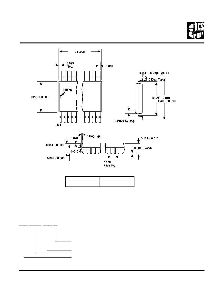
24-pin SOIC package
Ideal for RISC or CISC systems such as 486, Pentium,
PowerPC, etc., requiring multiple CPU and BUS
clocks.
Pentium is a trademark of Intel Corporation.
PowerPC is a trademark of Motorola Corporation.
NOTE: THIS DATA SHEET, ICS9158-04, IS AN ADDENDUM TO THE EXISTING
ICS9158 DATA SHEET. ALL INFORMATION IN THIS DATA SHEET SUPERSEDES THE
DATA FOUND IN THE ORIGINAL ICS9158 DATA SHEET.
ICS reserves the right to make changes in the device data identified in this publication
without further notice. ICS advises its customers to obtain the latest version of all
device data to verify that any information being relied upon by the customer is current
and accurate.
2
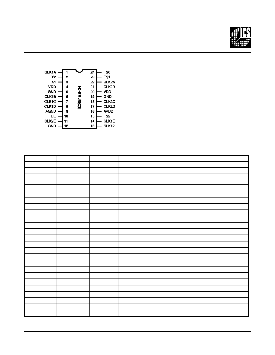
ICS9158-04
Pin Configuration
24-Pin SOIC
Pin Description
* Input pin has internal pull-up to VDD.
PIN NUMBER
PIN NAME
TYPE
DESCRIPTION
1
CLK1A
OUT
CPU clock output.
2
X2
OUT
Crystal connection output, which includes output crystal load capacitance.
3
X1
IN
Crystal connection input, which includes crystal load capacitance and
feedback bias for a nominal 14.31818 MHz parallel-resonance 12pF crystal.
4
VDD
PWR
Digital POWER SUPPLY.
5
GND
PWR
Digital GROUND.
6
CLK1B
OUT
CPU clock output.
7
CLK1C
OUT
CPU clock output.
8
CLK1D
OUT
CPU clock output.
9
AGND
PWR
ANALOG GROUND.
10
OE
IN
OUTPUT ENABLE. Tristates all outputs when low.*
11
CLK2E
OUT
2X CPU clock output.
12
GND
PWR
Digital GROUND.
13
CLK12
OUT
CPU clock output.
14
CLK1E
OUT
CPU clock output.
15
FS2
OUT
CPU clock frequency select 2.*
16
AVDD
PWR
ANALOG power supply.
17
CLK2D
OUT
2X CPU clock output.
18
CLK2C
OUT
2X CPU clock output.
19
GND
PWR
Digital GROUND.
20
VDD
PWR
Digital POWER SUPPLY.
21
CLK2B
OUT
2X CPU clock output.
22
CLK2A
OUT
2X CPU clock output.
23
FS1
IN
CPU clock frequency select #1.*
24
FS0
IN
CPU clock frequency select #0.*