Äîêóìåíòàöèÿ è îïèñàíèÿ www.docs.chipfind.ru
Integrated
Circuit
Systems, Inc.
General Description
Features
ICS9159C-02
The ICS9159C-02 generates all clocks required for high
speed RISC or CISC microprocessor systems such as 486,
Pentium, PowerPC, etc. Four different reference frequency
multiplying factors are externally selectable with smooth
frequency transitions. These multiplying factors can be
customized for specific applications. A test mode is provided
to drive all clocks directly.
High drive BCLK outputs provide typically greater than
1V/ns slew rate into 30pF loads. PCLK outputs provide
typically better than 1V/ns slew rate into 20pF loads while
maintaining
+/-
5% duty cycle.
Generates up to four processor and six bus clocks, plus
disk, keyboard and reference clocks
Synchronous clocks skew matched to 250ps window on
PCLKs and 500ps window on BCLKs
Test clock mode eases system design
Custom configurations available:
Output frequency ranges to 100 MHz on options
Selectable multiplying and processor/bus ratios
Stop clock control stops clock glitch-free; available as
mask option
3.0V - 5.5V supply range
28-pin SOIC package
Applications
Ideal for high-speed RISC or CISC systems such as
486, Pentium, PowerPC, etc.
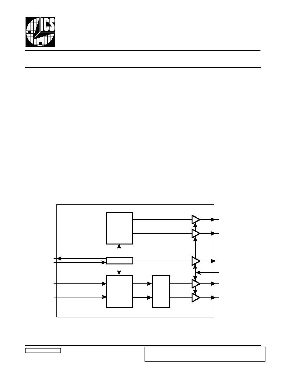
XTAL OSC
BCLK(0:5)
PCLK(0:3)
OEN
REF(0:1)
KEYBD
DISK
SYNC
REG
PLL
CLOCK
GEN
PLL
CLOCK
GEN
X2
X1
FS0
FS1
9159-02 Rev D 062397
Block Diagram
Pentium is a trademark of Intel Corporation
PowerPC is a trademark of Motorola Corporation
Frequency Generator and Integrated Buffer for PENTIUM
TM
ICS reserves the right to make changes in the device data identified in this publication
without further notice. ICS advises its customers to obtain the latest version of all
device data to verify that any information being relied upon by the customer is current
and accurate.
2
ICS9159C-02
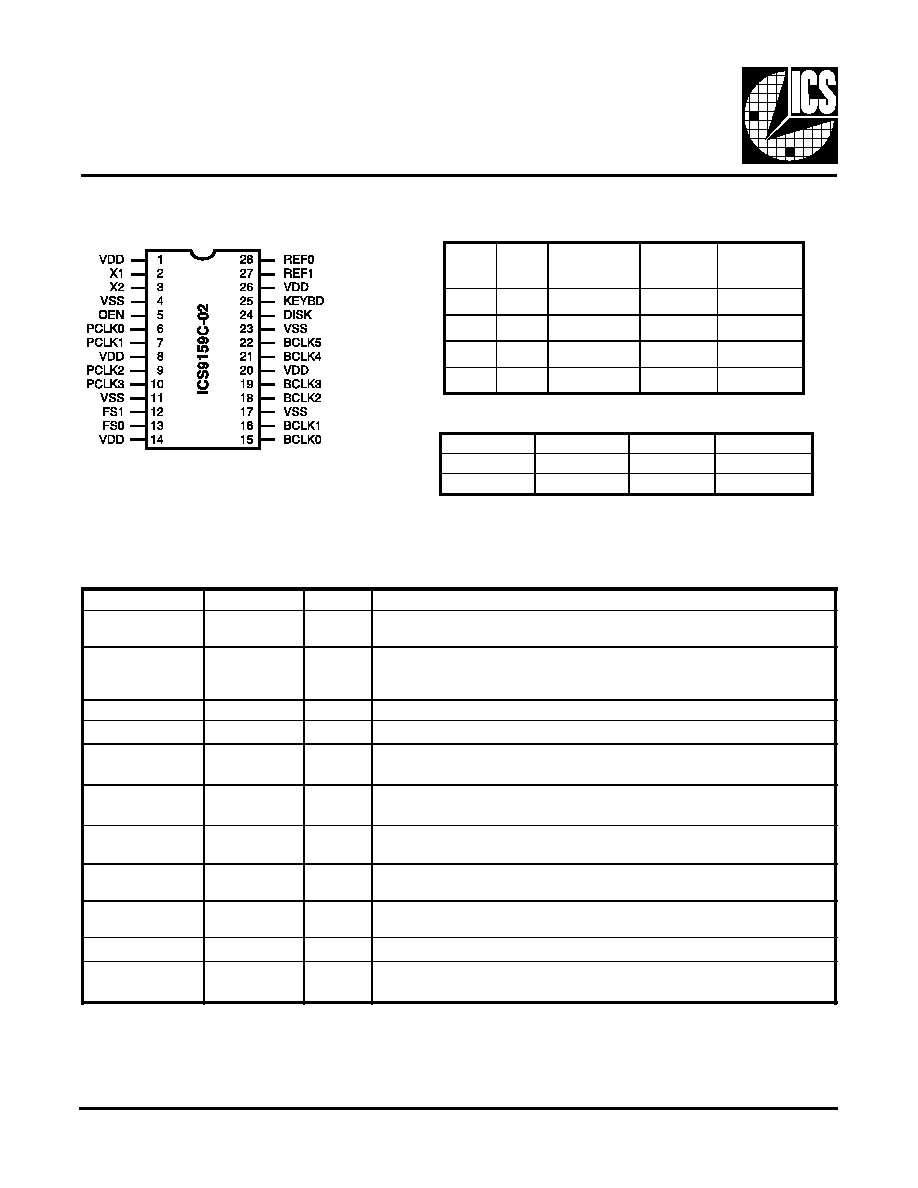
Pin Configuration
Pin Descriptions
Functionality
*VCO range is limited from 60 - 200 MHz
PCLK(0,3)
BCLK(0,5)
DISK
KEYBD
VCO/2
PCLK/2
24 MHz
12 MHz
TCLK/2
TCLK/4
TCLK/4
TCLK/8
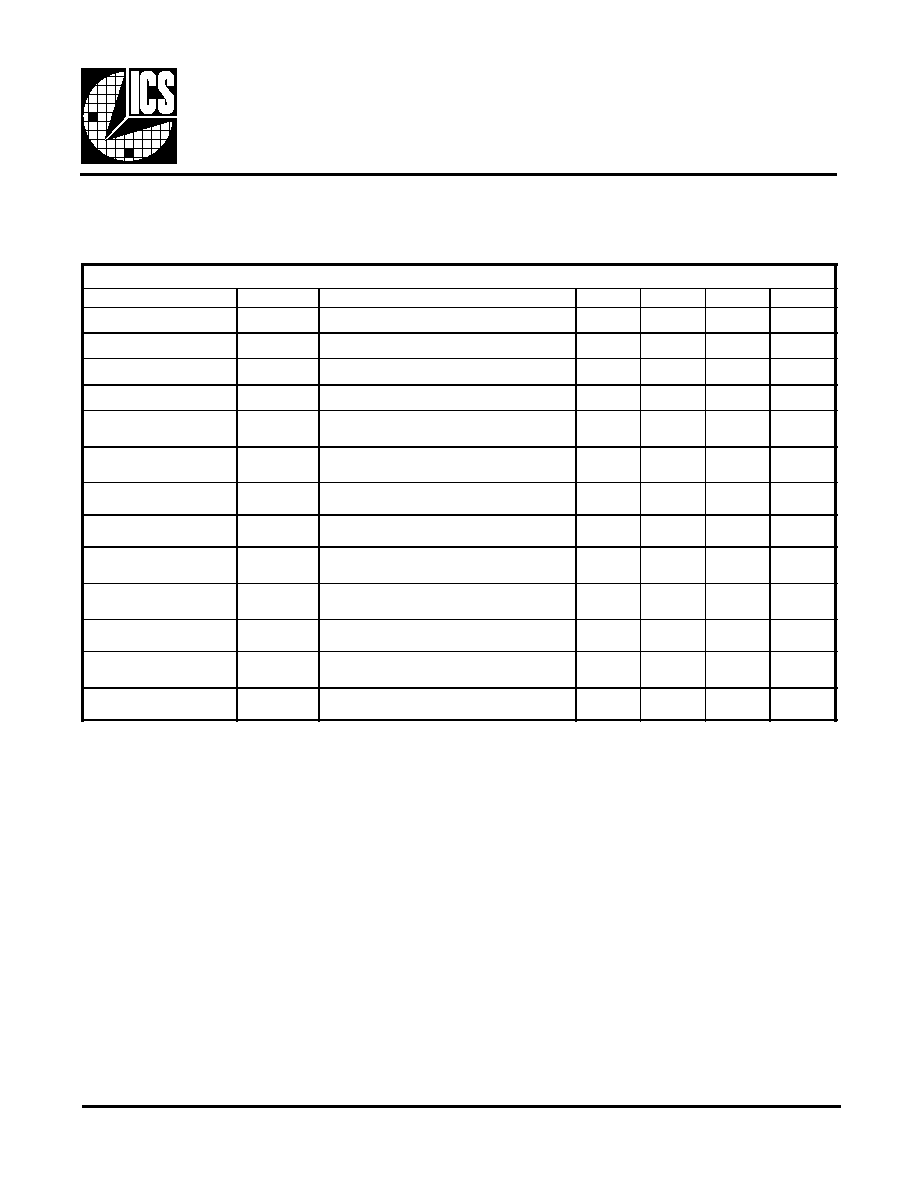
PIN NUMBER
PIN NAME
TYPE
DESCRIPTION
1, 8, 14,
20, 26
VDD
PWR
Power for logic, PCLK and fixed frequency output buffers.
2
X1
IN
XTAL or external reference frequency input. This input includes
XTAL load capacitance and feedback bias for a 12 - 16 MHz
crystal, nominally 14.31818 MHz.
3
X2
OUT
XTAL output which includes XTAL load capacitance.
4, 11, 17, 23
VSS
PWR
Ground for logic, PCLK and fixed frequency output buffers.
6, 7, 9, 10
PCLK(0:3)
OUT
Processor clock outputs which are a multiple of the input reference
frequency as shown in the table above.
13, 12
FS(0:1)
IN
Frequency multiplier select pins. See table above. These inputs have
internal pull-up devices.
15, 16, 18 19,
21, 22
BCLK(0:5)
OUT
Bus clock outputs are fixed at one half the PCLK frequency.
5
OEN
IN
OEN tristates all outputs when low. This input has an internal pull-
up device.
24
DISK
OUT
The DISK controller clock is fixed at 24 MHz
(with 14.318 MHz input).
25
KEYBD
OUT
The KEYBD clock is fixed at 12 MHz (with 14.318 MHz input).
28, 27
REF(0:1)
OUT
REF is a buffered copy of the crystal oscillator or reference input
clock nominally 14.31818 MHz.
Note: BCLK buffers cannot be supplied with 5 volts (pins 14 and 20) if CPU and fixed frequencies (pins 1, 8, and 26) are being
supplied with 3.3 volts
28-Pin SOIC
FS1
FS0
*VCO
X1, REF
(MHz)
CPU
(MHz)
0
0
118/17xX1
14.318
50(49.7)
0
1
65/7xX1
14.318
66.6(66.5)
1
0
92/11xX1
14.318
60(59.9)
1
1
Test mode
TCLK
TCLK/2
3
ICS9159C-02
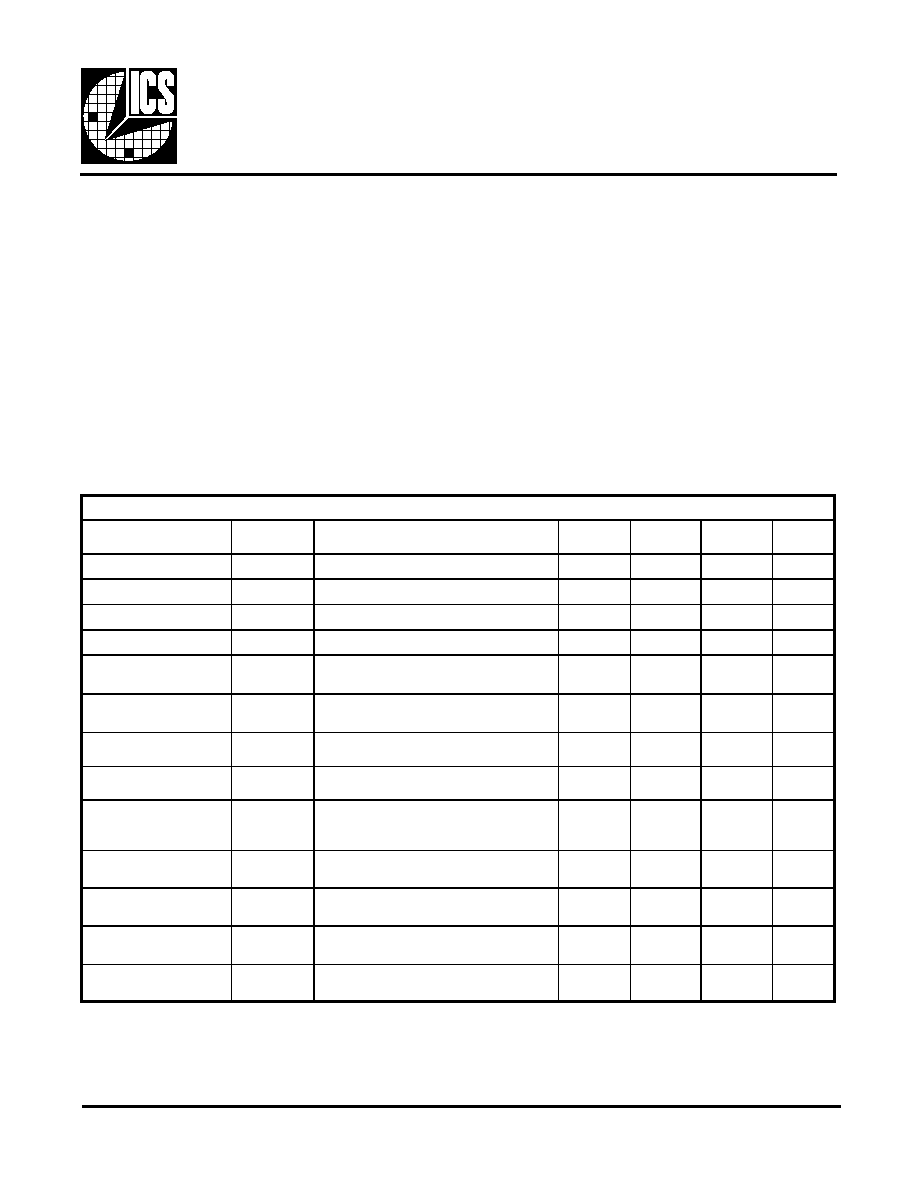
Absolute Maximum Ratings
Electrical Characteristics at 3.3 V
Stresses above those listed under Absolute Maximum Ratings may cause permanent damage to the device. These ratings are
stess specifications only and functional operation of the device at these or any other conditions above those listed in the
operational sections of the specifications is not implied. Exposure to absolute maximum rating conditions for extended periods
may affect product reliability.
Supply Voltage ......................................................................................... 7.0 V
Logic Inputs ..................................................... GND - 0.5 V to VDD + 0.5 V
Ambient .................................................... Operating Temperature0 to +70 C
Storage Temperature .................................................................. 65 to +150 C
V
DD
= 3.0 - 3.7 V, T
A
= 0 - 70
o
C unless otherwise stated
Note 1: Parameter is guaranteed by design and characterization. Not 100% tested in production.
DC Characteristics
PARAMETER
SYMBOL
TEST CONDITIONS
MIN
TYP
MAX
UNITS
Input Low Voltage
V
IL
-
-
0.2V
DD
V
Input High Voltage
V
IH
0.7V
DD
-
-
V
Input Low Current
I
IL
V
IN
=0V
-28.0
-10.5
-
mA
Input High Current
I
IH
V
IN
=V
DD
-5.0
-
5.0
mA
Output Low Current
1
I
OL
V
OL
=0.8V for PCLKS & BCLKS
30.0
47.0
-
mA
Output High Current
1
I
OH
VOL=2.0V for PCLKS & BCLKS
-
-66.0
-42.0
mA
Output Low Current
1
I
OL
VOL=0.8V for fixed CLKs
25.0
38.0
-
mA
Output High Current
1
I
OH
VOL=2.0V for fixed CLKs
-
-47.0
-30.0
mA
Output Low Voltage
1
V
OL
I
OL
=15mA for PCLKS & BCLKS
-
0.3
0.4
V
Output High
Voltage
1
V
OH
I
OH
=-30mA for PCLKS & BCLKS
2.4
2.8
-
V
Output Low Voltage
1
V
OL
I
OL
=12.5mA for fixed CLKs
-
0.3
0.4
V
Output High
Voltage
1
V
OH
I
OH
=-20mA for fixed CLKs
2.4
2.8
-
V
Supply Current
I
DD
@66.5 MHz all outputs unloaded
-
55
110
mA
4
ICS9159C-02
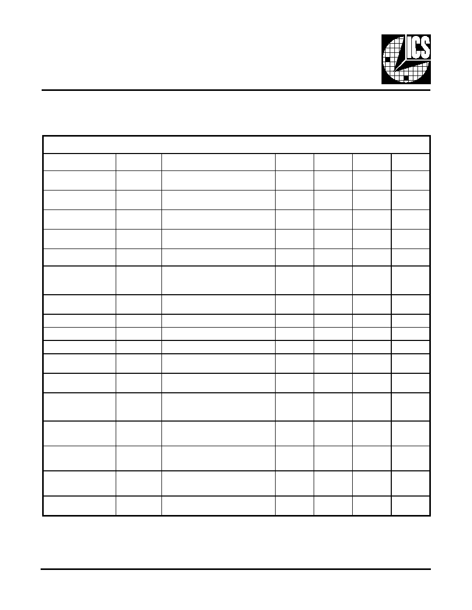
Electrical Characteristics at 3.3 V
V
DD
= 3.0 - 3.7 V, T
A
= 0 - 70
o
C unless otherwise stated
Note 1: Parameter is guaranteed by design and characterization. Not 100% tested in production.
AC Characteristics
PARAMETER
SYMBOL
TEST CONDITIONS
MIN
TYP
MAX
UNITS
Rise Time
1
T
r1
20pF load, 0.8 to 2.0V
PCLK & BCLK
-
0.9
1.5
ns
Fall Time
1
T
f1
20pF load, 2.0 to 0.8V
PCLK & BCLK
-
0.8
1.4
ns
Rise Time
1
T
r2
20pF load, 20% to 80%
PCLK & BCLK
-
1.5
2.5
ns
Fall Time
1
T
f2
20pF load, 80% to 20%
PCLK & BCLK
-
1.4
2.4
ns
Duty Cycle
1
D
t
20pF load @ VOUT=1.4V
45
50
55
%
Jitter, One Sigma
1
T
j1s1
PCLK & BCLK Clocks;
Load=20pF, FOUT>25 MHz
-
50
150
ps
Jitter, Absolute
1
T
jab1
PCLK & BCLK Clocks;
Load=20pF, FOUT >25 MHz
-250
-
250
ps
Jitter, One Sigma
1
T
j1s2
Fixed CLK; Load=20pF
-
1
3
%
Jitter, Absolute
1
T
jab2
Fixed CLK; Load=20pF
-5
2
5
%
Input Frequency
1
F
i
12.0
14.318
16.0
MHz
Logic Input
Capacitance
1
C
IN
Logic input pins
-
5
-
pF
Crystal Oscillator
1
Capacitance1
C
INX
X1, X2 pins
-
18
-
pF
Power-on Time
1
t
on
From V
DD
=1.6V to 1st
crossing of 66.5 MHz V
DD
supply ramp<40ms
-
2.5
4.5
ms
Frequency Settling
Time
1
t
s
From 1st crossing of
acquisition to <1% settling
-
2.0
4.0
ms
Clock Skew
Window
1
T
sk1
PCLK to PCLK;
Load=20pF; @1.4V
-
150
250
ps
Clock Skew
Window
T
sk2
BCLK to BCLK;
Load=20pF; @1.4V
-
300
500
ps
Clock Skew
Window
1
T
sk3
PCLK to BCLK;
Load=20pF; @1.4V
1
2.6
5
ns
5
ICS9159C-02
Electrical Characteristics at 5.0 V
Note 1: Parameter is guaranteed by design and characterization. Not 100% tested in production.
D C C haracteristics
PARAMETER
SYMBOL
TEST CONDITIONS
MIN
TYP
MAX
UNITS
Input Low Voltage
V
IL
-
-
0.8
V
Input High Voltage
V
IH
2.4
-
-
V
Input Low Current
I
IL
V
IN
=0V
-45
-15
-
mA
Input High Current
I
IH
V
IN
=V
DD
-5.0
-
5.0
mA
Output Low Current
1
I
OL
V
OL
=0.8V; for PCLKS & BCLKS
36.0
62.0
-
mA
Output High Current
1
I
OH
V
OH
=2.0V; for PCLKS & BCLKS
-
-152
-90.0
mA
Output Low Current
1
I
OL
V
OL
=0.8V; for fixed CLKs
30.0
50.0
-
mA
Output High Current
1
I
OH
VOL=2.0V; for fixed CLKs
-
-110.0
-65.0
mA
Output Low Voltage
1
V
OL
I
OL
=20mA; for PCLKS & BCLKS
-
0.25
0.4
V
Output High Voltage
1
V
OH
I
OH
=-70mA; for PCLKS & BCLKS
2.4
4.0
-
V
Output Low Voltage
1
V
OL
I
OL
=15mA; for fixed CLKs
-
0.2
0.4
V
Output High Voltage
1
V
OH
I
OH
=-50mA; for fixed CLKs
2.4
4.7
-
V
Supply Current
I
DD
@66.5 MHz; all outputs unloaded
-
80.0
160.0
mA
V
DD
= 4.5 - 5.5 V, T
A
= 0 - 70
o
C unless otherwise stated