
Micro Networks 324 Clark Street Worcester, MA 01606 tel: 508-852-5400 fax: 508-852-8456 www.micronetworks.com
M2006-01
Preliminary Specifications
1
Micro Networks
An Integrated Circuit Systems Company
ISO 9001
Registered
ISO 9001
Registered
M2006-01
Frequency Synthesizer
APPLICATIONS
SONET / SDH / 10GbE System
Synchronization
Add / Drop Muxes, Access and Edge
Switches
Line Card System Clock Cleaner /
Translator
Optical Module Clock Cleaner / Translator
DESCRIPTION
The M2006-01 integrates a high performance Phase Locked
Loop (PLL) with a Voltage Controlled SAW Oscillator (VCSO)
to provide a low jitter Frequency Synthesizer in a 9mm x
9mm surface mount package.
The internal high "Q" SAW filter provides low jitter signal
performance and determines the output frequency of the
VCSO.
Selecting between two differential LVPECL clocks or one
single-ended LVCMOS / LVTTL clock provides the input
reference signal to the Frequency Translator. The maximum
input frequency is 700MHz.
The M2006-01 will default to a multiplying factor of 32 on
power-up. The multiplying factor can be changed by serially
programming the input and feedback dividers via the
configuration logic.
A differential LVPECL signal provides the output clock for
the device. A second differential output which can be
programmed to divide the output frequency by a factor of 4
is also available. The output frequency can be momentarily
increased or decreased to add or subtract one net output
clock cycle by asserting the ADD_CLK or DROP_CLK
inputs, respectively.
An external loop filter sets the PLL bandwidth which can be
optimized to provide jitter attenuation of the input reference
clock. A phase slope limiting feature, which reduces phase
build-out in order to meet GR-253 MTIE upon an input
transient, can be manually selected by asserting the PSL
input. The phase slope limiting feature is automatically
activated whenever a new input reference clock is selected.
The frequency agility, bandwidth control, and phase slope
limiting features make the M2006-01 ideal for use as a clock
jitter attenuator, frequency translator, and clock frequency
generator in OC-3 through OC-192 applications.
Inputs, V
I
:
................................................. -0.5 to V
CC
+0.5V
Output, V
O
:
................................................. -0.5 to V
CC
+0.5V
Supply Voltage, V
CC
: ......................................................... 4.6 V
Storage Temperature, T
STO
: ............................ -45�C to +100�C
ABSOLUTE MAX RATINGS
Output Clock Frequency up to 700MHz
Intrinsic Jitter <1ps rms (12kHz - 50MHz)
Automatic Phase Slope Limiting
Dual Differential Inputs
Input Compatible with LVPECL, LVDS,
HSTL, SSTL, etc.
Triple Input MUX
Configurable Input and Feedback Dividers
Tunable Loop Filter Response
Two Differential LVPECL outputs
Single 3.3V Supply
Small 9mm x 9mm SMT Package
FEATURES
Stresses beyond those listed under Absolute Maximum Ratings may cause
permanent damage to the device. These ratings are stress specifications only.
Functional operation of product at these conditions or any conditions beyond
those listed in the DC Characteristics or AC Characteristics is not implied.
Exposure to absolute maximum rating conditions for extended periods may
affect product reliability.
Micro Networks 324 Clark Street Worcester, MA 01606 tel: 508-852-5400 fax: 508-852-8456 www.micronetworks.com
M2006-01
Preliminary Specifications
2
Micro Networks
An Integrated Circuit Systems Company
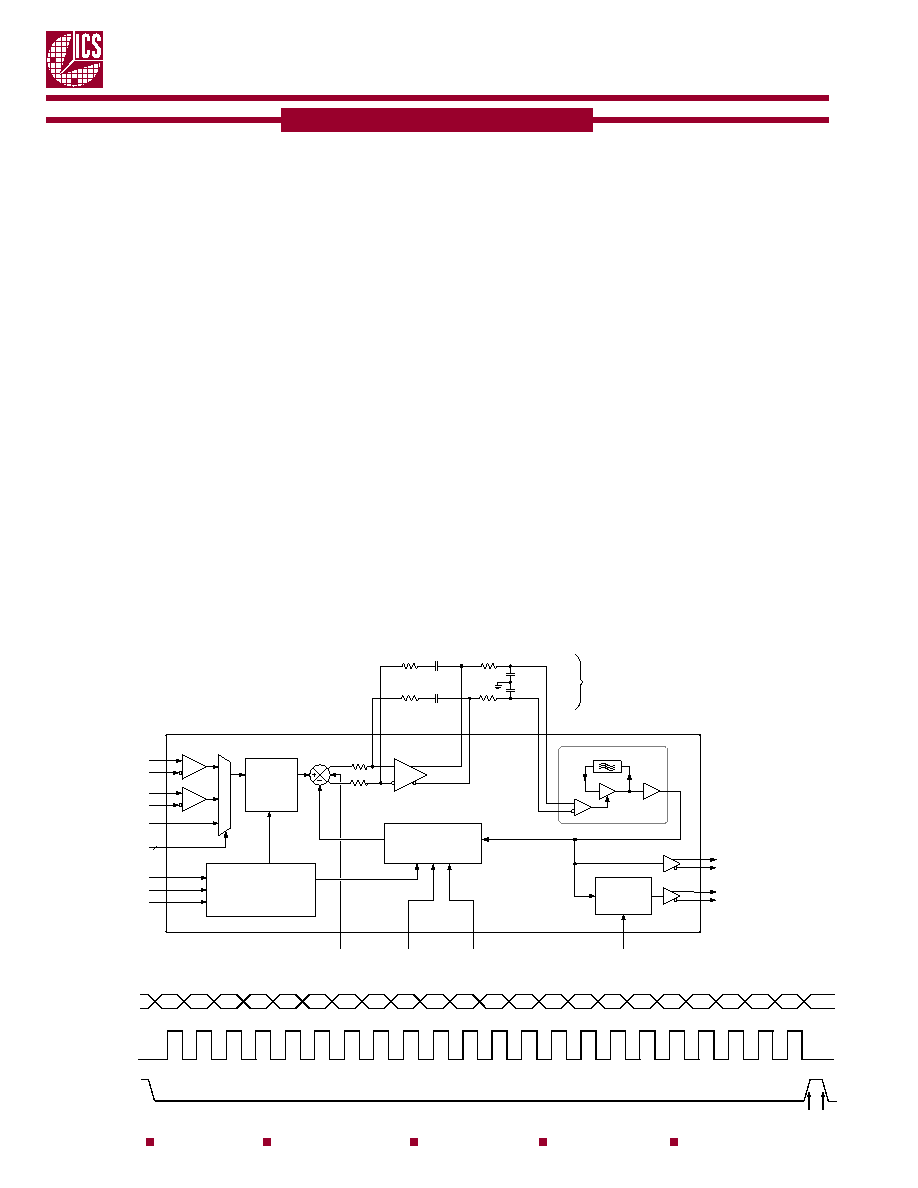
FUNCTIONAL BLOCK DIAGRAM
The internal PLL will adjust the VCSO output
frequency to be M (feedback divider) divided by R
(input divider) times the selected input reference clock
frequency. Note that the ratio of M/R times input
frequency must be such that it falls within the "lock"
range of the VCSO. The M divider (10-bits) can be
programmed for a maximum value of 1023 and a
minimum value of 4. The R divider (9-bits) can be set
to a maximum value of 511 and a minimum value of 1.
There are two differential LVPECL outputs (Fout 0,
Fout 1) which operate at the VCSO frequency. When
P1 is HIGH the Fout 1 output will operate at 1/4 the
VCSO frequency and when P1 is LOW Fout 1 output
operates at the VCSO frequency.
The relationship between the VCSO frequency, the M
and R dividers, and the input REF_CLK is defined as
follows:
F VCSO = F REF_CLK x M / R
On power-up the R and M dividers are set to 1 and
32, respectively.
The input reference clock is selected from DIF_CLK 0,
DIF_CLK 1, or REF_CLK by selecting the appropriate
REF_SEL 0 and REF_SEL 1 inputs. When a new
reference is selected the M2006-01 will automatically
switch to the "phase slope limiting" mode to control
the phase build-out of the output clocks.
The ADD_CLK and DROP_CLK inputs increments or
decrements the M (feedback) divider for one phase
detector cycle. This results in a momentary increase or
decrease in output frequency and an extra or missing
output clock cycle relative to the input reference clock.
The "phase slope limiter" is used to ensure MTIE
compliance. The PSL input provides manual control.
When PSL is HIGH, the output phase slope is limited by
changing the phase detector gain to a non-linear function.
.
The M2006-01 is serially programmed via a 3 wire interface.
Refer to the timing diagram below (labeled "SERIAL
PROGRAMMING") for the following explanation.
Serial operation begins at point "(a)", when S_LOAD is LOW;
the shift register is loaded one bit at-a-time by sampling
the S_DATA bits with the rising edge of S_CLOCK.
Divider load occurs at point "(b)" , when S_LOAD transitions
from LOW to HIGH; all of the data in the shift register is
loaded into the R and M dividers.
Latch occurs at point "(c)", on the HIGH-to-LOW transition of
S_LOAD; divider values will not be affected by serial input.
(If S_LOAD is held HIGH, any S_DATA input is passed directly
to the R and M dividers on each rising edge of S_CLOCK.)
Note: T1 and T0, which are used for test automation, must be set to 0. T2 is set to 1 for normal bandwidth, 0 for narrow bandwidth.
S_DATA T2 T1 T0 R8 R7 R6 R5 R4 R3 R2 R1 R0 M9 M8 M7 M6 M5 M4 M3 M2 M1 M0
S_CLOCK
S_LOAD
SERIAL PROGRAMMING
M2006-01
SAW Delay Line
Phase
Shifter
VCSO
C
POST
C
POST
VC
nVC
R
POST
nOP_OUT
OP_OUT
R
POST
R
LOOP
R
LOOP
C
LOOP
C
LOOP
R
IN
R
IN
OP_IN
nOP_IN
M Divider
M = 3-1024
Power-Up Default = 32
Serial
Configuration
Register
Phase
Detector
Loop Filter
Amplifier
External
Loop Filter
Components
FOUT0
nFOUT0
S_DATA
S_CL
OCK
S_LOAD
R Divider
R = 1-511
Power-Up
Default = 1
MUX
00
REF_SEL1:0
REF_CLK
DIF_REF1
nDIF_REF1
DIF_REF0
nDIF_REF0
01
1X
2
ADD_CLK
DROP_CLK
P Divider
P = 1 ( P1 = 0 )
or 4 ( P1 = 1 )
FOUT1
nFOUT1
P1
PSL
(a) (b) (c)

Micro Networks 324 Clark Street Worcester, MA 01606 tel: 508-852-5400 fax: 508-852-8456 www.micronetworks.com
M2006-01
Preliminary Specifications
3
Micro Networks
An Integrated Circuit Systems Company
FUNCTIONAL DESCRIPTION
LOOP FILTER
FIGURE 2
The M2006-01 requires the use of an external loop
filter via the provided filter pins. Due to the
differential design, the implementation requires two
identical RC filters as shown in Figure 2.
Rloop
Rloop
Cloop
Cloop
Cpost
Cpost
Rpost
Rpost
TABLE 1. EXAMPLE OF LOOP FILTER VALUES
Input Reference Frequency = 19.44MHz; VCSO Frequency = 622.0800MHz
PLL
Damping
R loop
C loop
R post
C post
Bandwidth
Factor
330Hz
2.0
3.9K
2.2�F
20k
250pF
1015Hz
2.0
12K
.22�F
20k
250pF
1975Hz
2.7
24K
.1�F
20k
250pF

Micro Networks 324 Clark Street Worcester, MA 01606 tel: 508-852-5400 fax: 508-852-8456 www.micronetworks.com
M2006-01
Preliminary Specifications
4
Micro Networks
An Integrated Circuit Systems Company
PIN DESCRIPTIONS
TABLE 2
Pin Number
Name
I/O
Configuration
Description
1, 2, 3
GND
GND
Power Supply Ground
4, 9
OP_IN, nOP_IN
Analog I/O
Used for external loop filter. See Figure 2.
5, 8
nOP_OUT, OP_OUT
Analog I/O
Used for external loop filter. See Figure 2.
6, 7
nVC, VC
Input
VCSO Differential Control Voltage Input Pair
10, 14, 26
GND
GND
Power Supply Ground
11, 19, 33
Vcc
Power
Positive Supply Pins
12, 13
FOUT1, nFOUT1
Output
Unterminated
Differential output, 3.3V LVPECL levels.
15, 16
FOUT0, nFOUT0
Output
Unterminated
Differential output, 3.3V LVPECL levels.
17
P1
Input
Pull - down
Determines the output divider value. LVCMOS / LVTTL
interface levels.
18
S_CLOCK
Input
Pull - down
Clocks in serial data present at S_DATA input into the
shift register on the rising edge of S_CLOCK.
LVCMOS / LVTTL interface levels.
20
S_DATA
Input
Pull - down
Shift register serial input. Data is sampled on the rising
edge of S_CLOCK. LVCMOS / LVTTL interface levels.
21
S_LOAD
Input
Pull - down
Controls transition of data from shift register into the
dividers. LVCMOS / LVTTL interface levels.
22, 29 REF_SEL1, REF_SEL0 Input Pull - down Selects between the different reference clock inputs as
the PLL reference source. LVCMOS / LVTTL interface
levels.
23
NDIF_CLK0
Input
Pull - up
Inverting differential clock input.
LVCMOS / LVTTL interface levels.
24
DIF_CLK0
Input
Pull - down
Non-inverting differential clock input. LVCMOS / LVTTL
interface levels.
25
REF_CLK
Input
Pull - down
Reference clock input. LVCMOS / LVTTL interface
levels.
27
NDIF_CLK1
Input
Pull - up
Inverting differential clock input. LVPECL levels.
28
DIF_CLK1
Input
Pull - down
Non-inverting differential clock input.
30
ADD_CLK
Input
Pull - down
Increases the output frequency by one output clock
cycle for a given input clock cycle. The added clock
occurs during the next input clock period following the
rising edge of ADD_CLK. Only one output clock can be
added for each input reference clock cycle. LVCMOS /
LVTTL interface levels.
31
DROP_CLK
Input
Pull - down
Decreases the output frequency by one output clock
cycle for a given input clock cycle. The deletion occurs
during the next input clock period following the rising
edge of DROP_CLK. Only one output clock can be
deleted for each input reference clock cycle. LVCMOS /
LVTTL interface levels.
32
PSL
Input
Pull - down
Asserting PSL (phase slope limiter) causes a decrease
in the loop bandwidth by reducing the phase detector
gain. LVCMOS / LVTTL interface levels.
34, 35, 36
DNC
No connection. Internal test pins must be left floating.

Micro Networks 324 Clark Street Worcester, MA 01606 tel: 508-852-5400 fax: 508-852-8456 www.micronetworks.com
M2006-01
Preliminary Specifications
5
Micro Networks
An Integrated Circuit Systems Company
TABLE 5
TABLE 4
PIN CHARACTERISTICS
Inputs
S_LOAD S_
CLOCK
S_DATA Conditions
L
Data
Serial input mode. Shift register loads state of S_DATA on each rising clock of
S_CLOCK. (However, serial input does not affect the values in the R and M dividers.)
L
Data Entire contents of the shift register are passed (all at once) to the R and M dividers.
L Data R and M divider values are latched.
L
X
X
Serial input does not affect the values in the R and M dividers.
H Data Serial input affects dividers: S_DATA passed directly to R and M dividers as it is clocked.
Note: L = Low; H = High; X = Don't care; = Rising Edge Transition; = Falling Edge Transition
TABLE 5C
Inputs
REF_SEL1
REF_SEL0
Reference
0
0
DIF_CLK0, nDIF_CLK0
0
1
DIF_CLK1, nDIF_CLK1
1
X
REF_CLK
REFERENCE SELECT FUNCTION TABLE
SERIAL MODE FUNCTION
Symbol
Parameter
Test Conditions
Min
Typical
Max
Units
C
IN
Input Capacitance
4
pF
R
PULLUP
Input Pullup Resistor
51
k
R
PULLDOWN
Input Pulldown Resistor
51
k