
M2006-03 Datasheet Rev 1.0
Page 1
Revision 011603
I n t e g r a t e d C i r c u i t S y s t e m s , I n c .
C o m m u n i c a t i o n s M o d u l e s
w w w. i c s t . c o m
t e l ( 5 0 8 ) 8 5 2 - 5 4 0 0
M2006-03
CMTS D
IRECT
C
ONVERSION
(Z
ERO
IF) C
LOCK
S
OURCE
Integrated
Circuit
Systems, Inc.
P r e l i m i n a r y I n f o r m a t i o n
G
ENERAL
D
ESCRIPTION
The M2006-03 is a VCSO (Voltage Controlled SAW
Oscillator) based clock generator
PLL designed for frequency
translation and jitter attenuation of
a master reference clock in a cable
modem termination system
(CMTS). External loop filter
components allow tailoring of the
PLL loop response. The M2006-03 includes a phase-
slope limiting feature to prevent disruptive output clock
phase changes upon input reference reselection.
F
EATURES
�
Integrated SAW (surface acoustic wave) delay line
�
VCSO center frequency of 491.52MHz
�
Jitter 9ps rms, typical, over 100Hz to 12kHz
Jitter 3ps rms, typical, over 12kHz to 1GHz
�
PLL phase slope limiter circuit
�
Single-ended reference inputs support LVCMOS,
LVTTL
�
All output clocks are differential LVPECL compatible
�
Two downstream clocks, frequency-selectable
�
One upstream clocks, frequency-selectable
�
REF_OUT always provides a 10.24MHz reference clock
�
All output rising edges aligned to within 1nsec of
selected input reference rising edge (unless M2_SEL = 1)
�
Output duty cycle 47-53% worse case
�
Single 3.3V power supply
�
Small 9 x 9 mm SMT (surface mount) package
P
IN
A
SSIGNMENT
(9 x 9 mm SMT)
Figure 1: Pin Assignment
S
IMPLIFIED
B
LOCK
D
IAGRAM
Figure 2: Simplified Block Diagram
Selectable Frequencies (MHz) for
M2006-03-491.5200
Input Ref. Clock:
2.048, 4.096, 10.24, or 20.48 MHz
VCSO Frequency:
491.52 MHz
Downstream Clock:
245.76 or 491.52 MHz
Upstream Clock:
40.96, 81.92, 163.84, or 491.52 MHz
Output Ref. Clock:
10.24 MHz
Table 1: Selectable Frequencies (MHz) for M2006-03-491.5200
M 2 0 0 6 - 0 3
( T o p V i e w )
18
17
16
15
14
13
12
11
10
28
29
30
31
32
33
34
35
36
1
2
3
4
5
6
7
8
9
V
CCA
GND
R
E
F
_
SEL
RE
F
_
CL
K0
RE
F
_
CL
K1
D
S
_C
LK
_S
E
L
nU
S
_
C
L
K
US
_
C
L
K
VC
C
US_CLK_SEL1
US_CLK_SEL0
nDS_CLK_1
DS_CLK_1
GND
nDS_CLK_0
DS_CLK_0
VCC
GND
VCC
nREF_OUT
REF_OUT
M1_SEL
M2_SEL
VCC
DNC
DNC
DNC
nOP
_
IN
OP_
O
U
T
VC
nV
C
nO
P
_
O
U
T
OP
_IN
GND
GND
GND
19
20
21
22
23
24
25
26
27
M2006-03-491.52
M2_SEL
Reference
Clock Input
(20.48,
10.24,
4.096, or
2.048MHz)
DS_CLK Pairs
(491.52 or
245.76MHz)
Frequency Multiplying
PLL
M1_SEL DS_CLK_SEL
US_CLK_SEL1:0
External Loop Filter
VSCO
REF
Divider
DS
Divider
US
Divider
REF_CLK Pair
(10.24MHz)
US_CLK Pair
(491.52, 163.84,
81.92, 40.96MHz)
MUX
0
1
M2006-03 CMTS Direct Conversion (Zero IF) Clock Source

M2006-03 Datasheet Rev 1.0
Page 2
Revision 011603
I n t e g r a t e d C i r c u i t S y s t e m s , I n c .
C o m m u n i c a t i o n s M o d u l e s
w w w. i c s t . c o m
t e l ( 5 0 8 ) 8 5 2 - 5 4 0 0
Integrated
Circuit
Systems, Inc.
M2006-03
CMTS D
IRECT
C
ONVERSION
(Z
ERO
IF) C
LOCK
S
OURCE
P r e l i m i n a r y I n f o r m a t i o n
D
ETAILED
B
LOCK
D
IAGRAM
Figure 3: Detailed Block Diagram
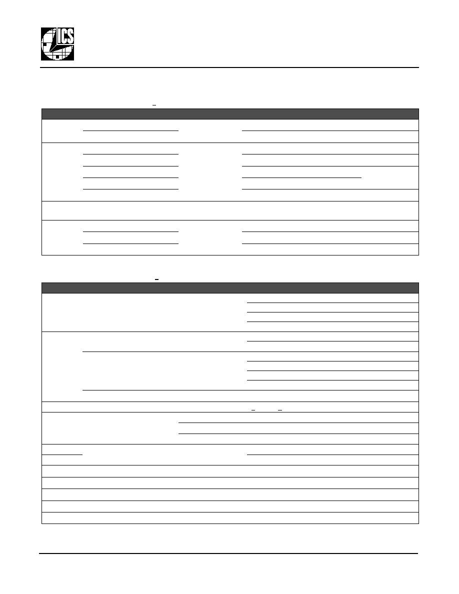
P
IN
D
ESCRIPTIONS
Number
Name
I/O
Configuration
Description
1, 2, 3, 10, 14, 26 GND
Ground
Power supply ground.
4, 9
OP_IN, nOP_IN
Input
Used for external loop filter. See
Figure 4
.
5, 8
nOP_OUT, OP_OUT
Output
6, 7
nVC, VC
Input
11, 19, 27, 28, 33 VCC
Power
Power supply connection, connect to +
3.3
V
12, 13
DS_CLK_0, nDS_CLK_0
Output
No internal terminator
Downstream clock output pairs.
Differential LVPECL.
15, 16
DS_CLK_1, nDS_CLK_1
20, 21
US_CLK_0, nUS_CLK
Upstream clock output pair. Differential LVPECL.
29, 30
nREF_OUT, REF_OUT,
Reference clock output pair. Differential LVPECL.
17, 18
US_CLK_SEL0,
US_CLK_SEL1
Input
Internal pull-down resistor
1
Upstream Divider controls. LVCMOS/LVTTTL.
For
US_CLK_SEL1:0
:
Logic
1
1
sets divider to
12
"
1
0
" " "
6
"
0
1
" " "
3
"
0
0
" " "
1
22
DS_CLK_SEL
Input
Internal pull-down resistor
1
Downstream Divider control. LVCMOS/LVTTTL:
Logic
1
sets divider to
2
Logic
0
sets divider to
1
23
REF_CLK1
Input
Internal pull-down resistor
1
NOTE 1: For typical values of internal pull-down resistors, see
DC Characteristics
,
Pull-down
on
pg. 5
.
Reference clock input 1. LVCMOS/LVTTTL.
24
REF_CLK0
Reference clock input 0. LVCMOS/LVTTTL.
25
REF_SEL
Input
Internal pull-down resistor
1
Reference clock input select. LVCMOS/LVTTTL:
Logic
1
selects
REF_CLK1
Logic
0
selects
REF_CLK0
31
M1_SEL
Input
M1 Divider control. LVCMOS/LVTTTL:
Logic
1
sets divider to 48 and
REF
Divider
to 2
Logic
0
sets divider to 24 and
REF
Divider
to 1
32
M2_SEL
Input
M2 Divider control. LVCMOS/LVTTTL:
Logic
1
sets divider to
5
Logic
0
sets divider to
1
34, 35, 36
DNC
Do Not Connect.
Table 2: Pin Descriptions
Phase
Locked
Loop
(PLL)
M2006-03
SAW Delay Line
Phase
Shifter
VCSO
C
POST
C
POST
VC
nVC
R
POST
nOP_OUT
OP_OUT
R
POST
R
LOOP
R
LOOP
C
LOOP
C
LOOP
R
IN
R
IN
OP_IN
nOP_IN
Phase
Detector
Loop Filter
Amplifier
External
Loop Filter
Components
DS_CLK_0
nDS_CLK_0
US_CLK_SEL1:0
US CLOCK
Divider
= 1,3,6 or 12
DS CLOCK
Divider
= 1 or 2
M1 Divider
M1 = 24 or 48
MUX
0
1
REF_SEL
REF_CLK0
REF_CLK1
M1_SEL
2
REF_OUT
nREF_OUT
DS_CLK_SEL
nDS_CLK_1
DS_CLK_1
US_CLK
nUS_CLK
M2 Divider
M2 = 1 or 5
M2_SEL
REF Divider
= 2 or 1

M2006-03 Datasheet Rev 1.0
Page 3
Revision 011603
I n t e g r a t e d C i r c u i t S y s t e m s , I n c .
C o m m u n i c a t i o n s M o d u l e s
w w w. i c s t . c o m
t e l ( 5 0 8 ) 8 5 2 - 5 4 0 0
M2006-03
CMTS D
IRECT
C
ONVERSION
(Z
ERO
IF) C
LOCK
S
OURCE
P r e l i m i n a r y I n f o r m a t i o n
Integrated
Circuit
Systems, Inc.
F
UNCTIONAL
D
ESCRIPTION
The M2006-03 is a PLL (Phase Locked Loop) based
clock generator that generates output clocks
synchronized to one of two selectable input reference
clocks.
An internal high "Q" SAW filter provides low jitter signal
performance and controls the output frequency of the
VCSO (Voltage Controlled SAW Oscillator). The VCSO
center frequency is an integer multiple of the input
reference frequency.
The M2006-03 is available with a
491.52
MHz VCSO
frequency that is specifically designed to support
DOCSIS modem applications. As such, the
M2006-03-491.520
(see
"Ordering Information"
on
pg. 6
)
accepts input reference frequencies of:
2.048
,
4.096
,
10.24
, and
20.48
MHz.
Input Reference
The selectable reference inputs are applied to the
REF_CLK1
and
REF_CLK0
input pins as necessary.
The
REF_SEL
pin selects the reference input:
�
REF_SEL
=
1
selects
REF_CLK1
.
�
REF_SEL
=
0
selects
REF_CLK0
.
The selected reference clock is supplied directly to the
phase detector of the PLL.
The PLL
The PLL (Phase Locked Loop) includes the phase
detector, the VCSO, and two feedback dividers (labeled
"M1 Divider" and "M2 Divider").
The product of the two feedback divider values equals
the overall feedback divider value "M".
The
M1_SEL
and
M2_SEL
pins select the individual M1 and
M2 divider values and, taken in combination, the overall
feedback divider value ("M").
"M" is used to divide the VCSO frequency so that it
matches the input reference frequency. The relationship
between the VCSO frequency, the M Divider, and the
input reference frequency is:
For the
M2006-03-491.5200
, which has a
VCSO frequency of
491.52
MHz, the four feedback divider values enable use
with these corresponding input reference frequencies:
Because both inputs to the phase detector have the
same frequency, the PLL can control the VCSO to keep
it locked to the input reference clock.
Post-PLL Dividers
The M2006-03 also features three post-PLL dividers:
the downstream ("DS") divider, the upstream ("US")
divider, and the output reference ("REF") divider.
The DS Divider:
Divides the VCSO frequency to produce
one of two downstream output frequencies (1/2 or 1/1 of
the VCSO frequency). The
DS_CLK_SEL
pin determines
the DS Divider value.
The US Divider:
Divides the VCSO frequency to produce
one of four upstream output frequencies (1/12, 1/6, 1/3
or 1/1 of the VCSO frequency). The
US_CLK_SEL1
and
US_CLK_SEL0
pins determine the US Divider value.
The REF Divider:
Used along with the M1 divider value
to ensure that the output system reference clock always
equals the VCSO frequency divided by 48. The
M1_SEL
pin determines the REF Divider value.
M2_SEL
M1_SEL
M2
Value
M1
Value
=
Overall Feedback
Divider "M" Value
1
1
5
48
240
1
0
24
120
0
1
1
48
48
0
0
24
24
Table 3: Combined Feedback Divider Selectors and Values
M1
M2 M
=
�
�
Fvcso
M
�
Fref_in
=
M2006-03-491.5200
M2006-03-491.5200
VSCO
Frequency (MHz)
M Feedback
Divider Value
=
Input Reference
Frequency (MHz)
491.52
240
2.048
120
4.096
48
10.24
24
20.48
Table 4: Feedback Divider Values and Input Reference Frequencies
DS_CLK_SEL
DS Value
M2006-03-491.5200
Downstream Output
Frequencies (MHz)
1
2
245.76
0
1
491.52
Table 5: Downstream Divider Selector, Values, and Frequencies
US_CLK_SEL1 US_CLK_SEL0
US Value
M2006-03-491.5200
Upstream Output
Frequencies (MHz)
1
1
12
40.96
1
0
6
81.92
0
1
3
163.84
0
0
1
491.52
Table 6: Upstream Divider Selectors, Values, and Frequencies
M2006-03-491.5200
M2006-03-491.5200
M1_SEL
REF
Value
VCSO
Frequency
(MHz)
M1
Value
REF
Value
=
REF Output
Frequency
(MHz)
1
1
491.52
48
1
10.24
0
2
24
2
Table 7: M1 Selector and REF Divider Values and Frequencies
�
�
�

M2006-03 Datasheet Rev 1.0
Page 4
Revision 011603
I n t e g r a t e d C i r c u i t S y s t e m s , I n c .
C o m m u n i c a t i o n s M o d u l e s
w w w. i c s t . c o m
t e l ( 5 0 8 ) 8 5 2 - 5 4 0 0
Integrated
Circuit
Systems, Inc.
M2006-03
CMTS D
IRECT
C
ONVERSION
(Z
ERO
IF) C
LOCK
S
OURCE
P r e l i m i n a r y I n f o r m a t i o n
Outputs
The M2006-03 provides a total of four differential
LVPECL output pairs:
�
Downstream -
The selected frequency is output from
DS_CLK_0
and from
DS_CLK_1
.
�
Upstream -
The selected frequency is output from
US_CLK
.
�
System reference -
The
10.24
MHz clock is output from
REF_OUT
.
External Loop Filter
To provide stable PLL operation, and thereby a low jitter
output clock, the M2006-03 requires the use of an
external loop filter. This is provided via the provided
filter pins (see
Figure 4
).
Due to the differential signal path design, the
implementation requires two identical complementary
RC filters as shown here.
Figure 4: External Loop Filter
C
POST
C
POST
VC
nVC
R
POST
nOP_OUT
OP_OUT
R
POST
R
LOOP
R
LOOP
C
LOOP
C
LOOP
OP_IN
nOP_IN
6
7
5
4
9
8
External Loop Filter Component Values for M2006-03-491.520
Input Reference
Clock Frequency
PLL
Bandwidth
Damping
Factor
R loop
C loop
R post C post
20.48MHz
1k
Hz
1.6
9.1
k
0.22
�F
20
k
250
pF
10.24MHz
1k
Hz
2.7
20
k
0.22
�F
20
k
250
pF
4.096MHz
1k
Hz
2.0
50
k
0.047
�F
20
k
250
pF
2.048MHz
1k
Hz
2.7
100
k
0.047
�F
20
k
250
pF
Table 8: External Loop Filter Component Values for M2006-03-491.520
A
BSOLUTE
M
AXIMUM
R
ATINGS
1
NOTE 1: Stresses beyond those listed under Absolute Maximum Ratings may cause permanent
damage to the device. These ratings are stress specifications only. Functional operation of product
at these conditions or any conditions beyond those listed in
Recommended Conditions of Operation
,
DC Characteristics
, or
AC Characteristics
is not implied. Exposure to absolute maximum rating
conditions for extended periods may affect product reliability.
Symbol Parameter
Rating
Unit
V
I
Inputs
-
0.5
to V
CC
+
0.5
V
V
O
Outputs
-
0.5
to V
CC
+
0.5
V
CC
Power Supply Voltage
4.6
T
S
Storage Temperature
-
45
to +
100
o
C
Table 9: Absolute Maximum Ratings
R
ECOMMENDED
C
ONDITIONS
OF
O
PERATION
Symbol Parameter
Min
Typ
Max
Unit
V
CC
Positive Supply Voltage
3.135
3.3
3.465
V
T
A
Ambient Operating Temperature
0
+
70
o
C
Table 10: Recommended Conditions of Operation
M2006-03 Datasheet Rev 1.0
Page 5
Revision 011603
I n t e g r a t e d C i r c u i t S y s t e m s , I n c .
C o m m u n i c a t i o n s M o d u l e s
w w w. i c s t . c o m
t e l ( 5 0 8 ) 8 5 2 - 5 4 0 0
M2006-03
CMTS D
IRECT
C
ONVERSION
(Z
ERO
IF) C
LOCK
S
OURCE
P r e l i m i n a r y I n f o r m a t i o n
Integrated
Circuit
Systems, Inc.
E
LECTRICAL
S
PECIFICATIONS
FOR M2006-03-491.520
DC Characteristics
Unless stated otherwise, V
CC
=
3.3
Volts +
5
%, T
A
=
0
o
C to
70
o
C, VCSO Frequency =
491.52
MHz, Outputs terminated with
50
to Vcc -
2
V
Symbol Parameter
Min
Typ
Max
Unit Test Conditions
Power Supply V
CC
Positive Supply
3.135
3.3
3.465
V
I
CC
Power Supply Current
162
mA
All Inputs
V
IH
Input High Voltage
REF_SEL,
M1_SEL, M2_SEL,
US_CLK_SEL0,
US_CLK_SEL1,
DS_CLK_SEL,
REF_CLK0, REF_CLK1
2
V
cc
+
0.3
V
V
IL
Input Low Voltage
-
0.3
0.8
V
I
IH
Input High Current
5
�A
I
IL
Input Low Current
-1
50
�A
C
in
Input Capacitance
4
pF
Pull-down
R
pulldown
Internal Pull-down
Resistor
(All Inputs)
51
k
Differential
Outputs
V
OH
Output High Voltage
US_CLK, nUS_CLK,
DS_CLK_0, nDS_CLK_0,
DS_CLK_1, nDS_CLK_1,
REF_OUT, nREF_OUT
V
cc
-
1.4
V
cc
-
1.0
V
V
OL
Output Low Voltage
V
cc
-
2.0
V
cc
-
1.7
V
V
P
-
P
Peak to Peak Output
0.6
0.85
V
Table 11: DC Characteristics
AC Characteristics
Unless implied otherwise, V
CC
=
3.3
Volts +
5
%, T
A
=
0
o
C to
70
o
C, VCSO Frequency =
491.52
MHz, Outputs terminated with
50
to Vcc -
2
V
Symbol Parameter
Min
Typ
Max
Unit Test Conditions
Input
Frequency
Range
F
IN
Input Frequency
REF_CLK0, REF_CLK1
20.48
MHz
M2_SEL=0, M1_SEL=0
10.24
MHz
M2_SEL=0, M1_SEL=1
4.096
MHz
M2_SEL=1, M1_SEL=0
2.048
MHz
M2_SEL=1, M1_SEL=1
Output
Frequency
Range
F
DS
_
OUT
Downstream Output
Frequency Range
DS_CLK_0, nDS_CLK_0,
DS_CLK_1, nDS_CLK_1
491.52
MHz
DS_CLK_SEL=0
245.76
MHz
DS_CLK_SEL=1
F
US
_
OUT
Upstream Output
Frequency Range
US_CLK, nUS_CLK
491.52
MHz
US_CLK_SEL1:0=00
163.84
MHz
US_CLK_SEL1:0=01
81.92
MHz
US_CLK_SEL1:0=10
40.96
MHz
US_CLK_SEL1:0=11
F
REF
_
OUT
Reference Output
REF_OUT, nREF_OUT
10.24
MHz
APR
VCSO Pull-Range
+
100
+
150
ppm
n
Single Side Band
Phase Noise
@
491.52
MHz
1
kHz Offset
-
72
dBc/Hz
10
kHz Offset
-
94
dBc/Hz
100
kHz Offset
-
123
dBc/Hz
J(t)
Jitter (rms)
Non-deterministic
9
ps
100
Hz to 1
2
kHz
3
ps
12
kHz to
1
GHz
t
PW
Output Duty Cycle, High Time
1
47
53
%
t
LOCK
PLL Lock Time
100
ms
t
R
Output Rise Time
1
325
450
500
ps
20
% to
80
%
t
F
Output Fall Time
1
325
450
500
ps
20
% to
80
%
t
S
Input to Output Skew
Rising Edge
1
ns
Table 12: AC Characteristics
NOTE 1: See
Parameter Measurement Information
on
pg. 6