 | –≠–ª–µ–∫—Ç—Ä–æ–Ω–Ω—ã–π –∫–æ–º–ø–æ–Ω–µ–Ω—Ç: M2020 | –°–∫–∞—á–∞—Ç—å:  PDF PDF  ZIP ZIP |

M2020/21 Datasheet Rev 1.0
Revised 30Jul2004
I n t e g r a t e d C i r c u i t S y s t e m s , I n c .
N e t w o r k i n g & C o m m u n i c a t i o n s
w w w. i c s t . c o m
t e l ( 5 0 8 ) 8 5 2 - 5 4 0 0
M2020/21
VCSO B
ASED
C
LOCK
PLL
Integrated
Circuit
Systems, Inc.
P r o d u c t D a t a S h e e t
G
ENERAL
D
ESCRIPTION
The M2020/21 is a VCSO (Voltage Controlled SAW
Oscillator) based clock jitter
attenuator PLL designed for clock
jitter attenuation and frequency
translation. The device is ideal for
generating the transmit reference
clock for optical network systems
supporting 2.5-10 GB data rates.
It can serve to jitter attenuate a
stratum reference clock or a recovered clock in loop
timing mode. The M2020/21 module includes a
proprietary SAW (surface acoustic wave) delay line as
part of the VCSO. This results in a high frequency,
high-Q, low phase noise oscillator that assures low
intrinsic output jitter.
F
EATURES
Integrated SAW (surface acoustic wave) delay line;
low phase jitter of < 0.5ps rms, typical (12kHz to 20MHz
or 50kHz to 80MHz)
Output frequencies of 15 to 700 MHz
*
LVPECL clock output (CML and LVDS options available)
Reference clock inputs support differential LVDS,
LVPECL, as well as single-ended LVCMOS, LVTTL
Loss of Lock (LOL) output pin
Narrow Bandwidth control input (NBW pin)
Hitless Switching (HS) options with or without Phase
Build-out (PBO) available for SONET (GR-253) /
SDH (G.813) MTIE and TDEV compliance during
reference clock reselection
Industrial temperature grade available
Single 3.3V power supply
Small 9 x 9 mm SMT (surface mount) package
P
IN
A
SSIGNMENT
(9 x 9 mm SMT)
Figure 1: Pin Assignment
* Specify VCSO center frequency at time of order.
S
IMPLIFIED
B
LOCK
D
IAGRAM
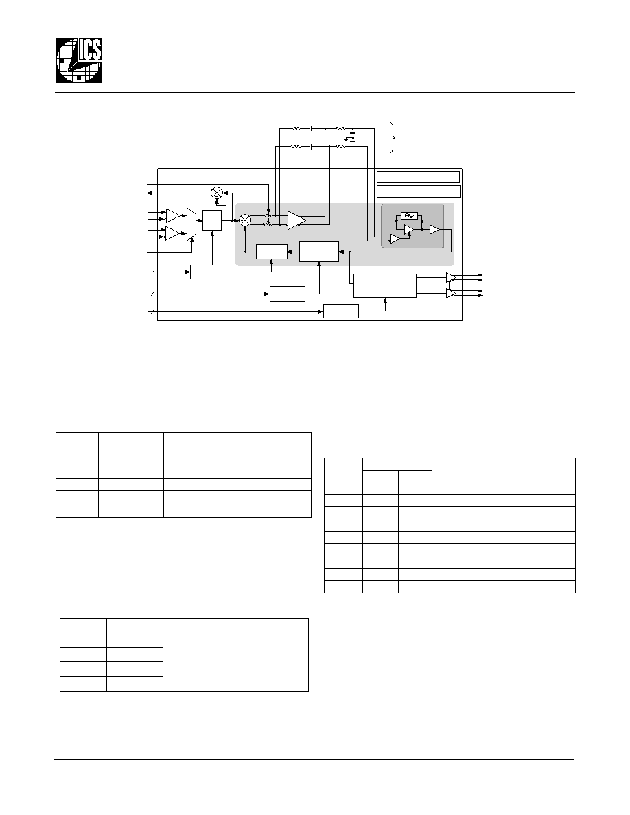
Figure 2: Simplified Block Diagram
Example I/O Clock Frequency Combinations
Using
M2020-11-622.0800 or M2021-11-622.0800
Input Reference
Clock
(MHz)
PLL Ratio
(Pin Selectable)
Output Clock
(MHz)
(M2020) (M2021)
19.44 or 38.88
(M2020) (M2021)
32 or 16
622.08
77.76
8
155.52
4
622.08
1
Table 1: Example I/O Clock Frequency Combinations
M 2 0 2 0
M 2 0 2 1
( T o p V i e w )
18
17
16
15
14
13
12
11
10
28
29
30
31
32
33
34
35
36
1
2
3
4
5
6
7
8
9
F
I
N
_
SEL
1
GN
D
P_
SE
L
2
DI
F
_RE
F
0
n
D
I
F
_RE
F
0
RE
F
_
S
E
L
DI
F
_RE
F
1
n
D
I
F
_RE
F
1
VC
C
P_SEL0
P_SEL1
nFOUT0
FOUT0
GND
nFOUT1
FOUT1
VCC
GND
FIN_SEL0
MR_SEL0
MR_SEL1
LOL
NBW
VCC
DNC
DNC
DNC
nOP
_
I
N
O
P
_O
UT
VC
nV
C
nOP
_
OU
T
OP
_
I
N
GN
D
GN
D
GN
D
19
20
21
22
23
24
25
26
27
M2020/21
Phase
Detector
FOUT0
nFOUT0
MR_SEL1:0
FIN_SEL1:0
R Div
(1, 4,
16, 64)
MUX
0
REF_SEL
DIF_REF0
nDIF_REF0
1
Mfin Divider
LUT
Mfin Div
(1, 4, 8, 32) or
( 1, 4, 8, 16)
P_SEL2:0
DIF_REF1
nDIF_REF1
LOL
VCSO
Loop
Filter
TriState
FOUT1
nFOUT1
P Divider
LUT
M Divider
(1, 4, 16, 64)
NBW
2
3
P Divider
FOUT0: 1, 4, 8, 32 or TriState
FOUT1: 1, 4, 8 or TriState
2
M / R Divider
LUT
M2020/21 VCSO Based Clock PLL
M2020/21 Datasheet Rev 1.0
2 of 10
Revised 30Jul2004
I n t e g r a t e d C i r c u i t S y s t e m s , I n c .
N e t w o r k i n g & C o m m u n i c a t i o n s
w w w. i c s t . c o m
t e l ( 5 0 8 ) 8 5 2 - 5 4 0 0
Integrated
Circuit
Systems, Inc.
M2020/21
VCSO B
ASED
C
LOCK
PLL
P r o d u c t D a t a S h e e t
P
IN
D
ESCRIPTIONS
Number
Name
I/O
Configuration
Description
1, 2, 3, 10, 14, 26
GND
Ground
Power supply ground connections.
4
9
OP_IN
nOP_IN
Input
External loop filter connections.
See Figure 5, External Loop Filter, on pg. 6.
5
8
nOP_OUT
OP_OUT
Output
6
7
nVC
VC
Input
11, 19, 33
VCC
Power
Power supply connection, connect to +
3.3
V.
12
13
FOUT1
nFOUT1
Output
No internal terminator
Clock output pair 1. Differential LVPECL.
15
16
FOUT0
nFOUT0
Output
No internal terminator
Clock output pair 0. Differential LVPECL.
17
18
25
P_SEL1
P_SEL0
P_SEL2
Input
Internal pull-down resistor
1
Note 1: For typical values of internal pull-down and pull-UP resistors, see
DC Characteristics on pg. 8.
Post-PLL , P divider selection. LVCMOS/LVTTL. See Table 5,
P Divider Look-Up Table (LUT),
on
pg. 3.
20
nDIF_REF1
Input
Biased to Vcc/2
2
Note 2: Biased toVcc/2, with 50k
to Vcc and 50k
to ground. See Differential Inputs Biased to VCC/2 on pg. 8.
Reference clock input pair 1. Differential LVPECL or LVDS.
Resistor bias on inverting terminal supports TTL or LVCMOS.
21
DIF_REF1
Internal pull-down resistor
1
22
REF_SEL
Input
Internal pull-down resistor
1
Reference clock input selection. LVCMOS/LVTTL:
Logic
1
selects
DIF_REF1, nDIF_REF1.
Logic
0
selects
DIF_REF0, nDIF_REF0
.
23
nDIF_REF0
Input
Biased to Vcc/2
2
Reference clock input pair 0. Differential LVPECL or LVDS.
Resistor bias on inverting terminal supports TTL or LVCMOS.
24
DIF_REF0
Internal pull-down resistor
1
27
28
FIN_SEL1
FIN_SEL0
Input
Internal pull-down resistor
1
I
nput clock frequency selection. LVCMOS/LVTTL.
See Table
3,
Mfin Divider Look-Up Table (LUT)
on
pg. 3.
29
30
MR_SEL0
MR_SEL1
Input
Internal pull-down resistor
1
M and R divider value selection. LVCMOS/ LVTTL.
See Table 4, M and R Divider Look-Up Table (LUT)
on
pg. 3.
31
LOL
Output
Loss of Lock indicator output. Asserted when internal PLL is
not tracking the input reference for frequency and phase.
3
Logic
1
indicates loss of lock.
Logic
0
indicates locked condition.
Note 3: See LVCMOS Output in
DC Characteristics on pg. 8.
32
NBW
Input
Internal pull-UP resistor
1
Narrow Bandwidth enable. LVCMOS/LVTTL:
Logic
1
- Narrow loop bandwidth
, R
IN
= 2100k
.
Logic
0
- Wide bandwidth
, R
IN
= 100k
.
34, 35, 36
DNC
Do Not Connect.
Internal nodes. Connection to these pins can cause erratic
device operation.
Table 2: Pin Descriptions
M2020/21 Datasheet Rev 1.0
3 of 10
Revised 30Jul2004
I n t e g r a t e d C i r c u i t S y s t e m s , I n c .
N e t w o r k i n g & C o m m u n i c a t i o n s
w w w. i c s t . c o m
t e l ( 5 0 8 ) 8 5 2 - 5 4 0 0
M2020/21
VCSO B
ASED
C
LOCK
PLL
P r o d u c t D a t a S h e e t
Integrated
Circuit
Systems, Inc.
D
ETAILED
B
LOCK
D
IAGRAM
Figure 3: Detailed Block Diagram
D
IVIDER
S
ELECTION
T
ABLES
Mfin Divider Look-Up Table (LUT)
The
FIN_SEL1:0
pins select the Mfin divider value, which
establishes the PLL clock multiplication ratio. Since the
VCSO frequency is fixed, this allows input reference
selection.
M and R Divider Look-Up Table (LUT)
The
MR_SEL1:0
pins select the M and R divider values,
which establish phase detector frequency. A lower
phase detector frequency improves jitter tolerance and
lowers loop bandwidth.
P Divider Look-Up Table (LUT)
The
P_SEL2:0
pins select the P divider values, which set
the output clock frequencies. A P divider of value of
1
will provide a
622.08MHz
output when using a
622.08MHz
VCSO, for example. P divider values of
4
,
8
, or
32
are
also available, plus a TriState mode. The outputs can be
placed into the valid state combinations as listed in
Table 5. (The outputs cannot each be placed into any of
the five available states independently.)
General Guidelines for M and R Divider Selection
∑
A lower phase detector frequency should be used for
loop timing applications to assure PLL tracking,
especially during GR-253 jitter tolerance testing. The
recommended maximum phase detector frequency
for loop timing mode is
19.44MHz
.
∑
When
LOL
is to be used for system health monitoring,
the phase detector frequency should be 5MHz or
greater. Low phase detector frequencies make
LOL
overly sensitive, and higher phase detector
frequencies make
LOL
less sensitive. The
LOL
pin
should not be used during loop timing mode.
Mfin Divider
LUT
Phase
Locked
Loop
(PLL)
M2020/21
SAW Delay Line
Phase
Shifter
VCSO
C
POST
C
POST
VC
nVC
R
POST
nOP_OUT
OP_OUT
R
POST
R
LOOP
R
LOOP
C
LOOP
C
LOOP
OP_IN
nOP_IN
Phase
Detector
Loop Filter
Amplifier
External
Loop Filter
Components
MR_SEL1:0
FIN_SEL1:0
MUX
0
REF_SEL
DIF_REF0
nDIF_REF0
1
P_SEL2:0
R
IN
DIF_REF1
nDIF_REF1
LOL
R Div
(1, 4,
16, 64)
P Divider
LUT
P Divider
(for FOUT0: 1, 4, 8, or 32),
(for FOUT1: 1, 4, or 8)
M and R Divider
LUT
NBW
M Div
(1, 4, 16, 64)
Mfin Divider
(1, 4, 8, 32 or
1, 4, 8, 16)
FOUT0
nFOUT0
TriState
FOUT1
nFOUT1
2
2
3
Hitless Switching (HS) Opt.
HS with Phase Build-out Opt.
FIN_SEL1:0
Mfin Value
Input Ref. Freq. (MHz)
1
M2020-yz-622.0800 or M2021-yz-622.0800
Note 1: Example with
M2020-yz-622.0800 or M2021-yz-622.0800
0
0
(M2020) (M2021)
32 or 16
19.44 or 38.88
0
1
8
77.76
1
0
4
155.52
1
1
1
622.08
Table 3: Mfin Divider Look-Up Table (LUT)
MR_SEL1:0
M
R
Description
0 0
1
Note 1: Do not use with FIN_SEL1:0=11; Maximum Phase Detector
Frequency=175MHz
1
1
Four sets of divider values to enable
adjustment of bandwidth and jitter
tolerance
0 1
4
4
1 0
16
16
1 1
64
64
Table 4: M and R Divider Look-Up Table (LUT)
P_SEL2:0
P Value
M2020-yz-622.0800 or M2021-yz-622.0800
Output Frequency (MHz)
FOUT0
FOUT1
for
FOUT0
for
FOUT1
0 0 0
32
1
19.44 622.08
0 0 1
32
4
19.44 155.52
0 1 0
1
1
622.08 622.08
0 1 1
4
1
155.52 622.08
1 0 0
8
8
77.76 77.76
1 0 1
4
4
155.52 155.52
1 1 0
8
4
77.76 155.52
1 1 1 TriState TriState
N/A N/A
Table 5: P Divider Look-Up Table (LUT)
M2020/21 Datasheet Rev 1.0
4 of 10
Revised 30Jul2004
I n t e g r a t e d C i r c u i t S y s t e m s , I n c .
N e t w o r k i n g & C o m m u n i c a t i o n s
w w w. i c s t . c o m
t e l ( 5 0 8 ) 8 5 2 - 5 4 0 0
Integrated
Circuit
Systems, Inc.
M2020/21
VCSO B
ASED
C
LOCK
PLL
P r o d u c t D a t a S h e e t
F
UNCTIONAL
D
ESCRIPTION
The M2020/21 is a PLL (Phase Locked Loop) based
clock generator that generates output clocks synchro-
nized to one of two selectable input reference clocks.
An internal high "Q" SAW delay line provides low jitter
signal performance and establishes the output
frequency of the VCSO (Voltage Controlled SAW
Oscillator). In a given M2020/21 device, the VCSO
center frequency is fixed. A common center frequency
is
622.08MHz,
for SONET for SDH optical network
applications. The VCSO center frequency is specified at
time of order (see "Ordering Information" on pg. 10).
The VCSO has a guaranteed tuning range of
±120 ppm
(commercial temperature grade).
Pin selectable dividers are used within the PLL and
for the output clock. This enables tailoring of device
functionality and performance. The Mfin divider controls
the overall PLL multiplication ratio and thus determines
the input reference clock (see Table 3, on pg. 3). The
M and R dividers control the phase detector frequency
(see Table 4). The P divider scales the VCSO output
enabling lower output frequency selections (Table 5).
The M2020/21 includes a Loss of Lock (
LOL
) indicator,
which provides status information to system
management software. A Narrow Bandwidth (
NBW
)
control pin is provided as an additional mechanism for
adjusting PLL loop bandwidth without affecting the
phase detector frequency.
Options are available for Hitless Switching (HS) with or
without Phase Build-out (PBO). They provide
SONET/SDH MTIE and TDEV compliance during a
reference clock reselection.
Allowance for a single-ended input has been facilitated
by a unique input resistor bias scheme, which is
described next and shown in Figure 4.
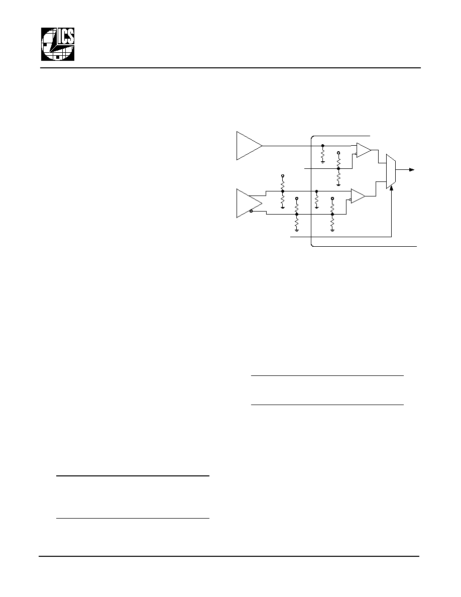
Input Reference Clocks
Two clock reference inputs and a selection mux are
provided. Either reference clock input can accept a
differential clock signal (such as LVPECL or LVDS) or
a single-ended clock input (LVCMOS or LVTTL on the
non-inverting input).
A single-ended reference clock on the unselected
reference input can cause an increase in output
clock jitter. For this reason, differential reference
inputs are preferred; interference from a differential
input on the non-selected input is minimal.
Configuration of a single-ended input has been
facilitated by biasing
nDIF_REF0
and
nDEF_REF1
to Vcc/2,
with 50k
to Vcc and 50k to ground. The input clock
structure, and how it is used with either
LVCMOS/LVTTL inputs or a DC- coupled LVPECL
clock, is shown in Figure 4
.
Figure 4: Input Reference Clocks
Differential Inputs
Differential LVPECL inputs are connected to both
reference input pins in the usual manner. The external
load termination resistors shown in Figure 4 (the 127
and 82
resistors) is ideally suited for both AC and DC
coupled LVPECL reference clock lines. These provide
the 50
load termination and the V
TT
bias voltage.
Single-ended Inputs
Single-ended inputs (LVCMOS or LVTTL) are
connected to the non-inverting reference input pin
(
DIF_REF0
or
DIF_REF1
). The inverting reference input pin
(
nDIF_REF0
or
nDIF_REF1
) must be left unconnected.
In single-ended operation, when the unused inverting
input pin (nDIF_REF0 or nDEF_REF1) is left floating (not
connected), the input will self-bias at VCC/2.
PLL Operation
The M2020/21 is a complete clock PLL. It uses a phase
detector and configurable dividers to synchronize the
output of the VCSO with the selected reference clock.
The PLL will work correctly, meaning it will phase-lock
the VCSO output to the input reference clock, when the
internal phase detector inputs are able to run at the
same frequency. This means the PLL dividers must be
set appropriately and a suitable reference frequency
must be chosen for the intended output frequency.
When the PLL is not set up appropriately, the VCSO is
forced to its upper or lower operating limit which is
typically about 250 ppm above or below the VCSO
center frequency (no more than 500 ppm above or
below).
MUX
0
REF_SEL
1
VCC
50k
50k
VCC
50k
50k
LVCMOS/
LVTTL
LVPECL
50k
50k
VCC
82
127
VCC
82
127
M2020/21
X
DIF_REF0
nDIF_REF0
DIF_REF1
nDIF_REF1

M2020/21 Datasheet Rev 1.0
5 of 10
Revised 30Jul2004
I n t e g r a t e d C i r c u i t S y s t e m s , I n c .
N e t w o r k i n g & C o m m u n i c a t i o n s
w w w. i c s t . c o m
t e l ( 5 0 8 ) 8 5 2 - 5 4 0 0
M2020/21
VCSO B
ASED
C
LOCK
PLL
P r o d u c t D a t a S h e e t
Integrated
Circuit
Systems, Inc.
In normal phase-locked condition, the instantaneous
phase error is measured by the phase detector and is
converted to charge pump current pulses. These
current pulses are then integrated by the external loop
filter to create a VCSO control voltage. The loop filter
acts as a low pass filter to remove unwanted reference
clock jitter above a determined frequency or PLL
bandwidth. For reference phase jitter frequencies within
the loop bandwidth, phase jitter amplitude is passed on
to the output clock according to the PLL loop frequency
response curve.
The relationship between the nominal VCSO center
frequency (Fvcso), the M divider, and the input
reference frequency (Fin) is:
The M, R, and Mfin dividers can be set by pin configura-
tion using the input pins
MR_SEL1
,
MR_SEL0
,
FIN_SEL1
,
and
FIN_SEL0
.
Post-PLL Divider
The M2020/21 also features a post-PLL (P) divider.
Through use of the P divider, the device's output
frequency (Fout) can be that of the VCSO (such as
622.08MHz
) or the VCSO frequency divided by
4
,
8
or
32
(common optical reference clocks in SONET and SDH
systems).
The
P_SEL2:0
pins select the value for the P divider. (See
Table 5 on pg. 3.)
Accounting for the P divider, the complete relationship
between the input clock reference frequency (Fin) and
output clock frequency (Fout) is defined as:
Due to the narrow tuning range of the VCSO (+120ppm
guaranteed), appropriate selection of all of the following
are required for the PLL be able to lock: VCSO center
frequency, input frequency, and divider selections.
TriState
The TriState feature puts the LVPECL output driver into
a high impedance state, effectively disconnecting the
driver from the
FOUT
and
nFOUT
pins of the device. A
logic
0
is then present on the clock net. The impedance
of the clock net is then set to 50
by the external circuit
resistors. (This is in distinction to a CMOS output in
TriState, in which case the net goes to a high
impedance and the logic value floats.) The 50
impedance level of the LVPECL TriState allows
manufacturing In-circuit Test to drive the clock net with
an external 50
generator to validate the integrity of
clock net and the clock load.
Any unused output (single-ended or differential) should
be left unconnected (floating) in system application.
This minimizes output switching current and therefore
minimizes noise modulation of the VCSO.
Narrow Bandwidth (NBW) Control Pin
A Narrow Loop Bandwidth control pin (
NBW
pin) is
included to enable adjustment of the PLL loop
bandwidth. In wide bandwidth mode (
NBW
=
0
), the
internal resistor Rin is 100k
. With the
NBW
pin
asserted (
NBW
=
1
), the internal resistor Rin is changed to
2100k
. This lowers the loop bandwidth by a factor of
about 21 (2100 / 100) and lowers the damping factor by
about 4.6 (the square root of 21), assuming the same
external loop filter component values.
Loss of Lock Indicator (LOL) Output Pin
Under normal device operation, when the PLL is locked,
the LOL Phase Detector drives
LOL
to logic
0
. Under
circumstances when the VCSO cannot fully phase lock
to the input (as measured by a greater than 4 ns
discrepancy between the feedback and reference clock
rising edges at the LOL Phase Detector) the
LOL
output
goes to logic 1. The
LOL
pin will return back to logic
0
when the phase detector error is less than 2 ns. The
loss of lock indicator is a low current LVCMOS output.
Guidelines for Using LOL
In a given application, the magnitude of peak-to-peak
jitter at the phase detector will usually increase as the R
divider is increased. If the
LOL
pin will be used to detect
an unusual clock condition, or a clock fault, the
MR_SEL1:0
pins should be set to provide a phase detector
frequency of
5MHz
or greater (the phase detector
frequency is equal to Fin divided by the R divider).
Otherwise, false
LOL
indications may result. A phase
detector frequency of
10MHz
or greater is desirable
when reference jitter is over
500ps
, or when the device is
used within a noisy system environment.
LOL
should not
be used when the device is used in a loop timing
application.
Example Frequency and Divider Combinations
Using M2021-yz-622.0800
Fvcso =
Fin x
Mfin x M/R
622.08
38.88
16 x (1/1, 4/4, etc.)
77.76
8 x (1/1, 4/4, etc.)
155.52
4 x (1/1, 4/4, etc.)
622.08
1 x (1/1, 4/4, etc.)
Table 6: Example I/O Clock Frequency Combinations
Fvcso
Fin Mfin
◊
M
R
----
◊
=
Fout
Fvcso
P
-------------------
=
Fin
M
Mfin
◊
R
P
◊
--------------------------
◊
=