MK1575-01
MDS 1575 G
1
Revision 060603
I n t e gra t e d C i r c u i t S y s t e m s
5 2 5 R a c e S t r e e t , S a n J o s e, C A 9 5 1 2 6
t e l ( 4 0 8 ) 2 9 5 - 9 8 0 0
w w w. i c s t . c o m
L
OW
C
OST
C
LOCK
R
ECOVERY
PLL
Description
The MK1575-01 is a low cost Phase Locked Loop
(PLL) designed for clock synthesis and synchronization
in cost sensitive applications. The device is optimized
to accept a low frequency reference clock to generate a
high frequency data or graphics pixel clock. External
loop filter components allow tailoring of loop frequency
response characteristics. For low jitter / phase noise
requirements refer to the MK2069 products.
Features
∑
Long-term output jitter <2 nsec over 10
µ
sec period
∑
External PLL clock feedback path enable "zero
delay" I/O clock skew configuration
∑
Selectable internal feedback divider provides popular
telecom and video clock frequencies (see tables
below)
∑
Can optionally use external feedback divider to
generate other output frequencies.
∑
Single 3.3V supply, low power CMOS
∑
Power down mode and output tri-state (pin OE)
∑
Packaged in 16 pin TSSOP
Pre-Configured Input/Output
Frequency Combinations:
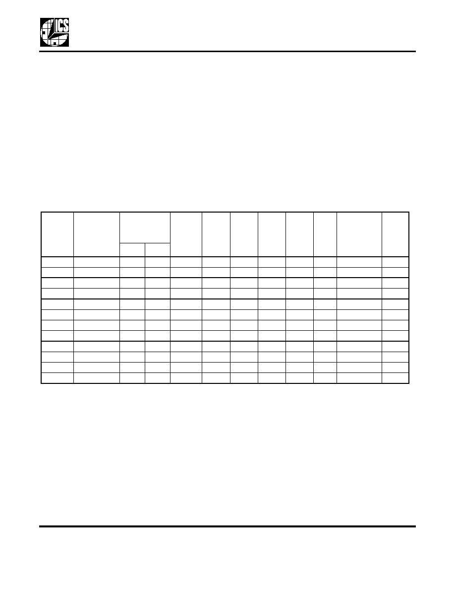
Telecom T/E Clock Modes (rising edge aligned):
Video Clock Modes (falling edge aligned):
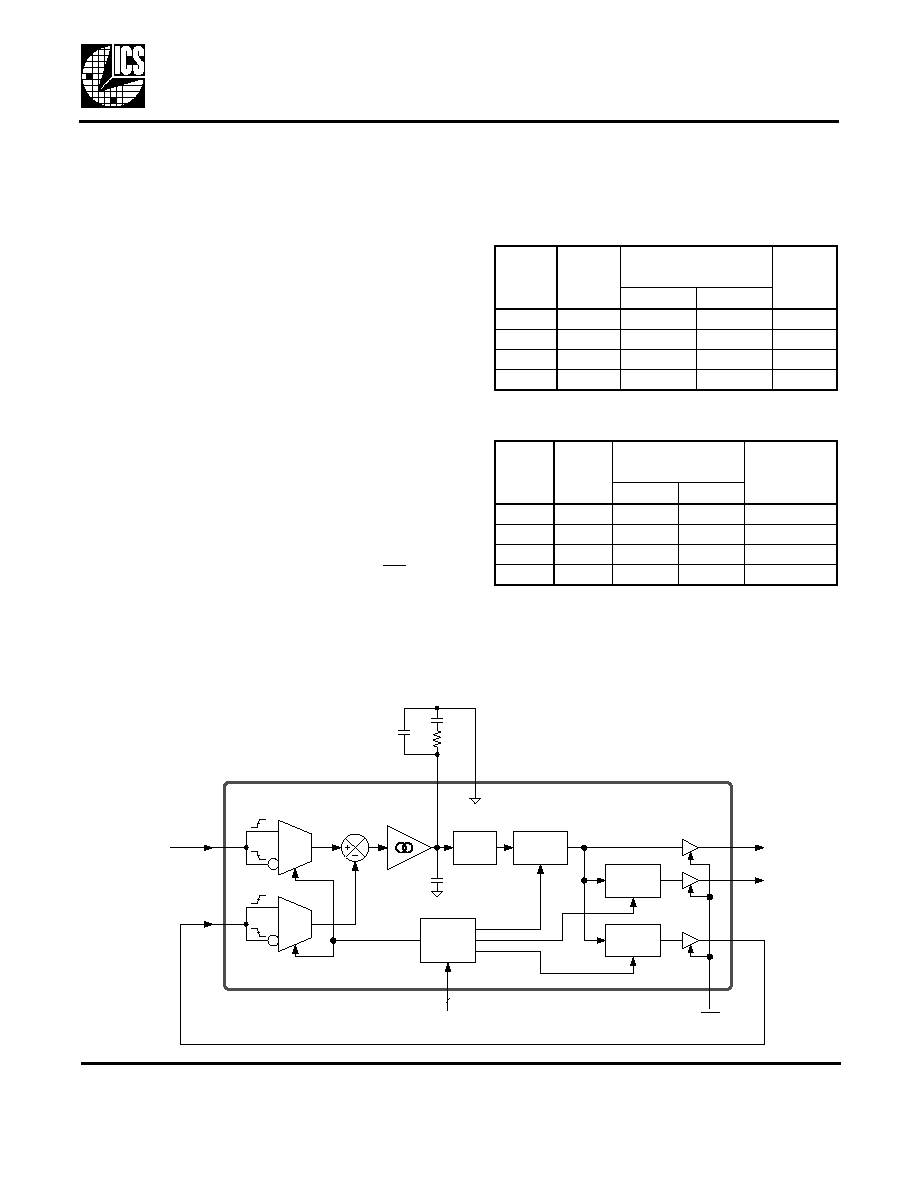
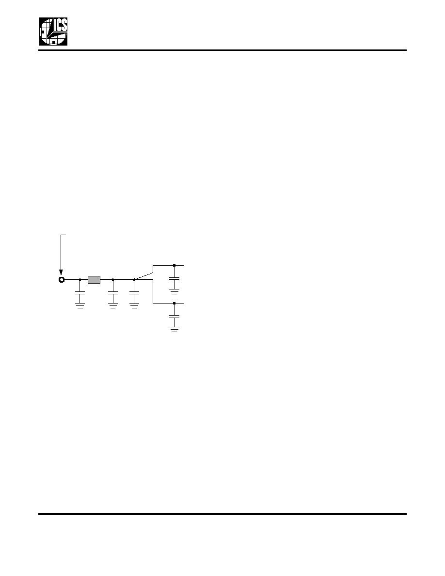
Block Diagram
The standard external clock feedback configuration is shown. Use this configuration for the pre-configured
input/output frequency combinations listed above.
Addr
FS2:0
Input
Clock
Output Clocks
(MHz)
Clock
Type
CLK1
CLK2
000
8 kHz
3.088
1.544
T1
001
8 kHz
16.384
2.048
E1
010
8 kHz
34.368
17.184
E3
011
8 kHz
44.736
22.368
T3
Addr
FS2:0
Input
Clock
(kHz)
Output Clocks
(MHz)
Clock
Type
CLK1
CLK2
100
15.625
54
27
PAL 601
101
15.734
54
27
NTSC 601
110
15.625
35.468
17.734
PAL 4xf
sc
111
15.734
28.636
14.318
NTSC 4xf
sc
REFIN
FBIN
CLK1
Clock Input
MUX
0
1
Charge
Pump
VCO
CHGP
VS
Divider
Phase
Detector
CHPR
MUX
0
1
C
B
R
S
C
S
FCLK
Divider
CLK2
Divider
Divider
LUT
CLK2
FCLK
FS2:0
3
External Feedback Clock Connection
OE
300 pF
L
OW
C
OST
C
LOCK
R
ECOVERY
PLL
MDS 1575 G
2
Revision 060603
I n t e gr a t e d C i r c u i t S y s t e m s
5 2 5 R a c e S t r e e t , S a n J o s e, C A 9 5 1 2 6
t e l ( 4 0 8 ) 2 9 5 - 9 8 0 0
w w w. i c s t . c o m
MK1575-01
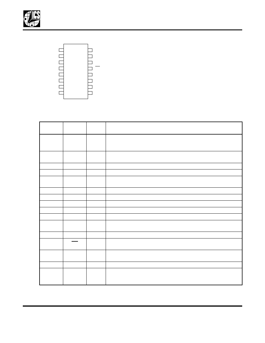
Pin Assignment
16 pin 4.40 mil body, 0.65 mil pitch TSSOP
Pin Descriptions
Detailed Mode Selection Table
12
1
11
2
10
REFIN
FBIN
3
9
FS0
4
VDDA
NC
5
VDDD
6
FCLK
7
FS1
8
GNDA
OE
CLK2
FS2
GNDD
CLK1
CHGP
CHPR
16
15
14
13
Pin
Number
Pin
Name
Pin
Type
Pin Description
1
REFIN
Input
Reference clock input. Connect the input clock to this pin. Can be
Rising or Falling edge triggered as per Detailed Mode Selection Table,
page 3.
2
FS0
Input
Frequency Selection Input bit 0, selects internal divider values as per
Detailed Mode Selection Table, page 3.
3
VDDA
Power
Power Supply connection for internal VCO and other analog circuits.
4
VDDD
Power
Power Supply connection for internal digital circuits and output buffers.
5
FS1
Input
Frequency Selection Input bit 1, selects internal divider values as per
Detailed Mode Selection Table, page 3.
6
GNDA
Ground
Ground connection for internal VCO and other analog circuits.
7
GNDD
Ground
Ground connection for internal digital circuits and output buffers.
8
CHGP
-
Loop filter connection, active node.
9
CHGR
-
Loop filter connection, reference node.
10
CLK1
Output
Output clock 1.
11
FS2
Input
Frequency Selection Input bit 2, selects internal divider values as per
Detailed Mode Selection Table, page 3.
12
CLK2
Output
Output clock 2.
13
OE
Input
Output Enable, tristates CLK1, CLK2, FCLK and powers down PLL
when high. Internal pull-up.
14
FCLK
Output
Feedback clock output, connect to FBIN for the pre-configured
frequency combinations listed in the tables on page 1.
15
NC
-
No internal connection, connect to ground.
16
FBIN
Input
Feedback clock input. Connect to CLK1, CLK2, FCLK, or the output of
an external feedback divider, depending on application. Refer to
document text for more information.
L
OW
C
OST
C
LOCK
R
ECOVERY
PLL
MDS 1575 G
3
Revision 060603
I n t e gr a t e d C i r c u i t S y s t e m s
5 2 5 R a c e S t r e e t , S a n J o s e, C A 9 5 1 2 6
t e l ( 4 0 8 ) 2 9 5 - 9 8 0 0
w w w. i c s t . c o m
MK1575-01
Refer to this table when not using the standard external clock feedback configuration shown on page 1.
Block Diagram, Showing Device Configuration Options
Address
FS2:0
Internal Divider Settings
FBIN, REFIN
Clock Edge
CLK1 Output
Frequency
Range
VS Divider
CLK2 Divider
FCLK Divider
000
64
2
386
Rising
1.5 - 5MHz
001
16
8
2048
Rising
6 - 20MHz
010
8
2
4296
Rising
12 - 40MHz
011
4
2
5592
Rising
24 - 80MHz
100
4
2
3456
Falling
24 - 80MHz
101
4
2
3432
Falling
24 - 80MHz
110
8
2
2270
Falling
12 - 40MHz
111
8
2
1820
Falling
12 - 40MHz
REFIN
FBIN
CLK1
Clock Input
MUX
0
1
Charge
Pump
VCO
CHGP
VS
Divider
Phase
Detector
CHPR
MUX
0
1
C
B
R
S
C
S
FCLK
Divider
CLK2
Divider
Divider
LUT
CLK2
FCLK
FS2:0
3
FB Divider
Optional External
Feedback Divider
Feedback Clock Options
(only connect one output)
OE
300 pF
L
OW
C
OST
C
LOCK
R
ECOVERY
PLL
MDS 1575 G
4
Revision 060603
I n t e gr a t e d C i r c u i t S y s t e m s
5 2 5 R a c e S t r e e t , S a n J o s e, C A 9 5 1 2 6
t e l ( 4 0 8 ) 2 9 5 - 9 8 0 0
w w w. i c s t . c o m
MK1575-01
Functional Description
The MK1575-01 is a PLL (phase locked loop) based
clock generator that generates output clocks
synchronized to an input reference clock. The device
can be used in the standard configuration as described
on page 1, or optionally can use an external divider in
the clock feedback path to produce other frequency
multiplication factors.
External components are used to control the PLL loop
response. The use of external loop components
enables a lower PLL loop bandwidth which is needed
when accepting low frequency input clocks such as
those listed in the tables on page 1.
PLL Clock Feedback Options
FCLK to FBIN
This is the standard configuration that is used for the
pre-configured input / output frequency combinations
listed on page 1. By including an external divider in the
feedback path ("FB Divider" in the Block Diagram of
page 3) the output clock frequency can be increased.
Refer to the Output Frequency Calculation table below.
CLK1 to FBIN
When no external feedback divider is used, this option
configures the device as a zero-delay buffer and the
frequency of CLK1 is the same as the input reference
clock. Including an external divider in the feedback path
will increase the output clock frequency. Refer to the
Output Frequency Calculation table below.
CLK2 to FBIN
Like the above configuration, this option configures the
device as a zero-delay buffer when no external
feedback divider is used, and the frequency of CLK2 is
the same as the input reference clock. Including an
external divider in the feedback path will increase the
output clock frequency. Refer to the Output Frequency
Calculation table below.
Frequency and Bandwith Calculations
Notes:
1) FB = 1 when no feedback divider is used.
2) Refer to the Detail Mode Selection Table on page 3 for possible divider combinations.
3) The VCO frequency needs to be considered in all applications (see table below)
4) The external loop filter also needs to be considered.
5) Minimum VCO frequency = 96 MHz
6) Maximum VCO frequency = 320 MHz
7) To minimize output jitter, use the highest possible VCO frequency allowed by the application
Feedback
Path
Option
Output Clock Frequency
CLK1
CLK2
FCLK
VCO
Frequency
"N" Factor
FCLK to
FBIN
CLK1 to
FBIN
CLK2 to
FBIN
f
IN
FB
◊
FCLK
◊
f
IN
FB
◊
FCLK
CLK2
----------------
◊
f
IN
FB
◊
f
IN
FB
◊
FCLK
2
◊
f
IN
FB
◊
VS
◊
VS
FCLK
◊
FB
◊
f
IN
FB
◊
f
IN
FB
◊
CLK2
----------------------
f
IN
FB
◊
FCLK
---------------------
VS
FB
◊
f
IN
FB
◊
CLK2
◊
f
IN
FB
◊
f
IN
FB
◊
CLK2
FCLK
----------------
◊
f
IN
FB
◊
CLK2
2
◊
VS
◊
VS
CLK2
◊
FB
◊
L
OW
C
OST
C
LOCK
R
ECOVERY
PLL
MDS 1575 G
5
Revision 060603
I n t e gr a t e d C i r c u i t S y s t e m s
5 2 5 R a c e S t r e e t , S a n J o s e, C A 9 5 1 2 6
t e l ( 4 0 8 ) 2 9 5 - 9 8 0 0
w w w. i c s t . c o m
MK1575-01
Setting PLL Loop Bandwidth and
Damping Factor
The frequency response of the MK1575-01 PLL may
be approximated by the following equation:
Normalized PLL Bandwidth
The associated damping factor is calculated as follows:
Damping factor,
Where:
K
O
= VCO gain in Hz/Volt
(use 340 MHz/V)
I
cp
= Charge pump current, 12.5
µ
A
N = Total feedback divide from VCO,
(Refer to N Value table, below)
C
S
= External loop filter capacitor in Farads
R
S
= Loop filter resistor in Ohms
The above bandwidth equation calculates the
"normalized" loop bandwidth which is approximately
equal to the - 3dB bandwidth. This approximate
calculation does not take into account the effects of
damping factor or the third pole imposed by C
P
. It does,
however, provide a useful approximation of filter
performance.
To prevent jitter on the output clocks due to modulation
of the PLL by the input reference frequency, the
following general rule should be observed:
In general, the loop damping factor should be 0.7 or
greater to ensure output stability. For video
applications, a low damping factor (0.7 to 1.0) is
generally desired for fast genlocking. For telecom
applications, a higher damping factor is usually
desirable. A higher damping factor will create less
passband gain peaking which will minimize the gain of
network clock wander amplitude. A higher damping
factor may also increase output clock jitter when there
is excess digital noise in the system application, due to
the reduced ability of the PLL to respond to, and
therefore compensate for, phase noise ingress.
Notes on setting the value of C
P
As another general rule, the following relationship
should be maintained between components C1 and C2
in the external loop filter:
Where:
C
B
= External bypass capacitor in Farads
Note that the MK1575-01 contains an internal 300 pF
filter cap which is connected in parallel with external
device C
B
. This helps to reduce output clock jitter. In
some applications external device C
B
will not be
required.
C
P
establishes a second pole in the PLL loop filter. For
higher damping factors (> 1), calculate the value of C
P
based on a C
S
value that would be used for a damping
factor of 1. This will minimize baseband peaking and
loop instability that can lead to output jitter.
C
P
also helps to damp VCO input voltage modulation
caused by the charge pump correction pulses. A C
P
value that is too low will result in increased output
phase noise at the phase detector frequency due to
this. In extreme cases where input jitter is high, charge
pump current is high, and C
P
is too small, the VCO
input voltage can hit the supply or ground rail resulting
in non-linear loop response.
The best way to set the value of C
P
is to use the filter
response software available on the ICS web site as
explained below.
R
S
K
O
I
CP
(
)
2
N
-----------------------------------------
=
R
S
2
--------
K
O
I
CP
C
S
N
-------------------------------------
=
PLL Bandwidth
f
Phase Detector
20
--------------------------------
C
P
C
S
20
------
=
C
P
C
B
300 pF
+
=
L
OW
C
OST
C
LOCK
R
ECOVERY
PLL
MDS 1575 G
6
Revision 060603
I n t e gr a t e d C i r c u i t S y s t e m s
5 2 5 R a c e S t r e e t , S a n J o s e, C A 9 5 1 2 6
t e l ( 4 0 8 ) 2 9 5 - 9 8 0 0
w w w. i c s t . c o m
MK1575-01
Loop Filter Response Software
ICS has an online and downloadable PC-based
programs available that simulate PLL loop response
characteristics. This software is available at:
http://www.icst.com/products/telecom/
This software can be used instead of the above
bandwidth and damping factor equations. The user
enters external loop filter component values and other
listed device characteristics. The program generates a
PLL frequency response graph, which translates to
jitter attenuation characteristics. Normalized bandwidth
(NBW) and damping factor values are also calculated.
Loop Filter Capacitor Type
Clock Jitter and input-to-output skew performance of
the MK1575-01 can be affected by loop filter capacitor
type. Cost vs. performance trade-offs can be made
when choosing capacitor types. Performance
differences are best determined through
experimentation.
Recommended capacitors can be found at
http://www.icst.com/products/telecom/
Example Loop Filter Component Values for Pre-Configured Frequency
Combinations Listed on Page 1.
Notes:
1) This loop filter selection is optimized for cost and component size. It provides stable clock outputs and
moderate input reference jitter attenuation. This configuration could be used when producing an internal
system clock, one which will not be used as a data transmit clock when locked to a recovered data clock.
2) This loop filter selection is optimized for low pass-band peaking. This configuration should be used when
generating data transmit clock that is locked to a recovered data clock. This will ensure that the data clock
conforms with Belcore GR-1244-CORE wander transfer specifications.
3) A loop bandwidth of 700 Hz and damping factor of 0.7 is typical for video genlock applications. This
combination assures minimal Hsync frequency modulation of the pixel clock yet genlocking.
Notes continued:
4) Example vendors and part numbers for above capacitor selections:
Addr
Input
Frequency
Output
Frequency
(MHz)
N Factor
R
S
C
S
C
B
Loop
BW
(-3dB)
Loop
Damp
Passband
Peaking
Notes
CLK1 CLK2
000
8 kHz
3.088
1.544
24704
15 k
1
µ
F
2.2 nF
363 Hz
2.5
0.19 dB
1
000
8 kHz
3.088
1.544
24704
6.8 k
10
µ
F
4.7 nF
199 Hz
4.46
0.06 dB
2
001
8 kHz
16.384
2.048
32768
18 k
1
µ
F
2.2 nF
425 Hz
3.24
0.12 dB
1
001
8 kHz
16.384
2.048
32768
8.2 k
10
µ
F
4.7 nF
181 Hz
4.67
0.05 dB
2
010
8 kHz
34.368 17.184
34368
18 k
1
µ
F
2.2 nF
405 Hz
3.16
0.13 dB
1
010
8 kHz
34.368 17.184
34368
8.2 k
10
µ
F
4.7 nF
173 Hz
4.56
0.06 dB
2
011
8 kHz
44.736 22.368
22368
12 k
1
µ
F
1 nF
390 Hz
2.62
0.17 dB
1
011
8 kHz
44.736 22.368
22368
6.8 k
10
µ
F
4.7 nF
219 Hz
4.69
0.05 dB
2
100
15.625 kHz
54
27
13824
10 k
0.068
µ
F 3.3 nF
758 Hz
0.72
2.16 dB
3
101
15.734 kHz
54
27
13728
10 k
0.068
µ
F 3.3 nF
760 Hz
0.73
2.15 dB
3
110
15.625 kHz
35.468 17.734
18160
10 k
0.068
µ
F 3.3 nF
760 Hz
0.73
2.15 dB
3
111
15.734 kHz
28.636 14.318
14560
10 k
0.068
µ
F 4.7 nF
721 Hz
0.7
2.42 dB
3

L
OW
C
OST
C
LOCK
R
ECOVERY
PLL
MDS 1575 G
7
Revision 060603
I n t e gr a t e d C i r c u i t S y s t e m s
5 2 5 R a c e S t r e e t , S a n J o s e, C A 9 5 1 2 6
t e l ( 4 0 8 ) 2 9 5 - 9 8 0 0
w w w. i c s t . c o m
MK1575-01
0.15
µ
F
Panasonic ECP-U1C154MA5 (SMT film type, 1206 size, available from DigiKey)
0.68
µ
F
Panasonic ECP-U1C684MA5 (SMT film type, 1206 size, available from DigiKey)
10
µ
F
MuRata GRM42-2X5R106K10
10 nF
Panasonic ECH-U1C103JB5 (SMT film type, 805 size, available from DigiKey)
33 nF
Panasonic ECH-U1C333JB5 (SMT film type, 1206 size, available from DigiKey)
Input-to-Output Skew Induced by Loop
Filter Leakage
Leakage across the loop filter, due to PCB
contamination or poor quality loop filter capacitors, can
increase input-to-output clock skew error. Concern
regarding input-to-output skew error is usually limited to
"zero delay" configurations, where CLK1 or CLK2 is
directly connected to FBIN. In sever cases of loop filter
leakage, however, output clock jitter can also be
increased.
The capacitors C
S
and C
P
in the external loop filter
maintain the VCO frequency control voltage between
charge pump pulses, which by design coincide with
phase detector events. VCO frequency or phase
adjustments are made by these charge pump pulses,
pumping current into (or out of) the external loop filter
capacitors to adjust the VCO control voltage as
needed. Like the capacitors, the CHGP pin (pin 8) is a
high-impedance PLL node; the charge pump is a
current source, which is high impedance by definition,
and the VCO input is also high impedance.
During normal (locked) operation, in the event of
current leakage in the loop filter, the charge pump will
need to deliver equal and opposite charge in the form
of longer charge pump pulses. The increased length of
the charge pump pulse will be translated directly to
increased input-to-output clock skew. This can also
result in higher output jitter due to higher reference
clock feedthrough (where the reference clock is f
REFIN
),
depending on the loop filter attenuation characterisitcs.
The Input-to-Output skew parameters in the DC
Electrical Specifications assume minimal loop filter
leakage. Additional skew due to loop filter leakage may
be calculated as follows:
Avoiding PLL Lockup
In some applications, the MK1575-01 VCO can "lock
up" at it's maximum operating frequency. To avoid this
problem observe the following rules:
1) Do not open the clock feedback path with the
MK1575-01 enabled. If the MK1575-01 is enabled and
does not get a feedback clock into pin FBIN, the output
frequency will be forced to the maximum value by the
PLL.
If an external divider is in the feedback path and it has
a delay before becoming active, hold the OE pin high
until the divider is ready to work. This could occur, for
example, if the divider is implemented in a FPGA.
Holding OE high powers down the MK1575-01 and
dumps the charge off the loop filter.
2) If an external divider is used in the feedback path,
use a circuit that can operate well beyond the intended
input clock frequency.
Power Supply Considerations
As with any integrated clock device, the MK1575-01
has a special set of power supply requirements:
∑
The feed from the system power supply must be
filtered for noise that can cause output clock jitter.
Power supply noise sources include the system
switching power supply or other system components.
The noise can interfere with device PLL components
such as the VCO or phase detector.
∑
Each VDD pin must be decoupled individually to
prevent power supply noise generated by one device
circuit block from interfering with another circuit
block.
∑
Clock noise from device VDD pins must not get onto
the PCB power plane or system EMI problems may
result.
This above set of requirements is served by the circuit
illustrated in the Optimum Power Supply Connection,
below. The main features of this circuit are as follows:
Leakage Induced I/O Skew (sec)
I
Leakage
I
CP
F
REFIN
◊
--------------------------------
=
L
OW
C
OST
C
LOCK
R
ECOVERY
PLL
MDS 1575 G
8
Revision 060603
I n t e gr a t e d C i r c u i t S y s t e m s
5 2 5 R a c e S t r e e t , S a n J o s e, C A 9 5 1 2 6
t e l ( 4 0 8 ) 2 9 5 - 9 8 0 0
w w w. i c s t . c o m
MK1575-01
∑
Only one connection is made to the PCB power
plane.
∑
The capacitors and ferrite chip (or ferrite bead) on
the common device supply form a lowpass `pi' filter
that remove noise from the power supply as well as
clock noise back toward the supply. The bulk
capacitor should be a tantalum type, 1
µ
F minimum.
The other capacitors should be ceramic type.
∑
The power supply traces to the individual VDD pins
should fan out at the common supply filter to reduce
interaction between the device circuit blocks.
∑
The decoupling capacitors at the VDD pins should be
ceramic type and should be as close to the VDD pin
as possible. There should be no vias between the
decoupling capacitor and the supply pin.
Optimum Power Supply Connection
Series Termination Resistor
Output clock PCB traces over 1 inch should use series
termination to maintain clock signal integrity and to
reduce EMI. To series terminate a 50
trace, which is a
commonly used PCB trace impedance, place a 33
resistor in series with the clock line as close to the clock
output pin as possible. The nominal impedance of the
clock output is 20
.
PCB Layout Recommendations
For optimum device performance and lowest output
phase noise, the following printed circuit board layout
recommendations should be observed.
1) Each 0.01µF power supply decoupling capacitor
should be mounted as close to the VDD pin as
possible. The PCB trace to VDD pin should be kept as
short as possible, as should the PCB trace to the
ground via. Distance of the ferrite chip and bulk
decoupling from the device is less critical.
2) The loop filter components (R
Z
, C
S
and C
B
) must
also be placed close to the CHGP and VIN pins. C
B
should be closest to the device. Coupling of noise from
other system signal traces should be minimized by
keeping traces short and away from active signal
traces. Use of vias should be avoided.
3) To minimize EMI the 33
series termination resistor,
if needed, should be placed close to the clock output.
4) Because each input selection pin includes an
internal pull-up device, those inputs requiring a logic
high state ("1") can be left unconnected. The pins
requiring a logic low state ("0") can be grounded.
C onnec tion V ia to
3.3V P ow er P lane
Ferrite
C hip
0.
1
F
BU
L
K
1 n
F
V D D
P in
0.
01
F
V D D
P in
0.
01
F
L
OW
C
OST
C
LOCK
R
ECOVERY
PLL
MDS 1575 G
9
Revision 060603
I n t e gr a t e d C i r c u i t S y s t e m s
5 2 5 R a c e S t r e e t , S a n J o s e, C A 9 5 1 2 6
t e l ( 4 0 8 ) 2 9 5 - 9 8 0 0
w w w. i c s t . c o m
MK1575-01
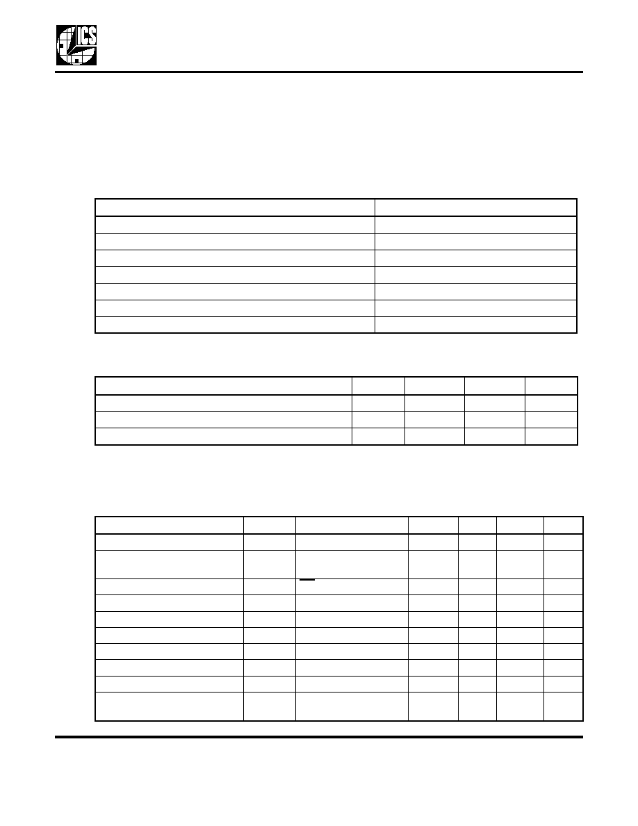
Absolute Maximum Ratings
Stresses above the ratings listed below can cause permanent damage to the MK1575-01. These ratings,
which are standard values for ICS commercially rated parts, are stress ratings only. Functional operation of
the device at these or any other conditions above those indicated in the operational sections of the
specifications is not implied. Exposure to absolute maximum rating conditions for extended periods can
affect product reliability. Electrical parameters are guaranteed only over the recommended operating
temperature range.
Recommended Operation Conditions
DC Electrical Characteristics
Unless stated otherwise, VDD = 3.3V ±5%, Ambient Temperature 0 to +70
∞
C
Item
Rating
Supply Voltage, VDD
7V
All Inputs and Outputs
-0.5V to VDD+0.5V
Ambient Operating Temperature (industrial version)
-40 to +85
∞
C
Ambient Operating Temperature (commercial version)
0 to +70
∞
C
Storage Temperature
-65 to +150
∞
C
Junction Temperature
175
∞
C
Soldering Temperature
260
∞
C
Parameter
Min.
Typ.
Max.
Units
Ambient Operating Temperature (industrial version)
-40
+85
∞
C
Ambient Operating Temperature (commercial version)
0
+70
∞
C
Power Supply Voltage (measured in respect to GND)
+3.15
+3.3
+3.45
V
Parameter
Symbol
Conditions
Min.
Typ.
Max.
Units
Operating Voltage
VDD
3.15
3.3
3.45
V
Supply Current
IDD
Clock outputs
unloaded, VDD = 3.3V
10
mA
Supply Current in Power Down
I
DD
OE = VDD
100
µ
A
Charge Pump Current
I
CP
12.5
µ
A
Input High Voltage
V
IH
2
V
Input Low Voltage
V
IL
0.8
V
Input High Current
I
IH
V
IH
= VDD
-10
+10
µ
A
Input Low Current
I
IL
V
IL
= 0
-10
+10
µ
A
Input Capacitance, except X1
C
IN
7
pF
Output High Voltage (CMOS
Level)
V
OH
I
OH
= -4 mA
VDD-0.4
V
L
OW
C
OST
C
LOCK
R
ECOVERY
PLL
MDS 1575 G
10
Revision 060603
I n t e gr a t e d C i r c u i t S y s t e m s
5 2 5 R a c e S t r e e t , S a n J o s e, C A 9 5 1 2 6
t e l ( 4 0 8 ) 2 9 5 - 9 8 0 0
w w w. i c s t . c o m
MK1575-01
AC Electrical Characteristics
Unless stated otherwise, VDD = 3.3V ±5%, Ambient Temperature 0 to +70
∞
C
Output High Voltage
V
OH
I
OH
= -8 mA
CLK1, CLK2
2.0
V
I
OH
= -4 mA
FCLK
2.0
V
Output Low Voltage
V
OL
I
OL
= 8 mA
CLK1, CLK2
0.4
V
I
OL
= -4 mA
FCLK
0.4
V
Short Circuit Current
I
OS
CLK1, CLK2
±43
mA
FCLK
±18
mA
Nominal Output Impedance
Z
OUT
20
Parameter
Symbol
Conditions
Min.
Typ.
Max.
Units
Input Clock Frequency
(into pins REFIN or FBIN)
f
REF
TBD
MHz
Internal VCO Frequency
f
VCO
96
320
MHz
Output Frequency
f
CLK
80
MHz
Output Rise Time
t
OR
0.8 to 2.0V
.6
1.1
ns
Output Fall Time
t
OF
2.0 to 0.8V
.6
1.1
ns
Output Clock Duty Cycle
t
DC
At VDD/2
45
50
55
%
Jitter, Absolute peak-to-peak
t
J
Single cycle
measurement;
Deviation from mean
150
ps
Long Term Timing Jitter, pk-pk
t
JLT
10
µ
S trigger delay
1.7
3.0
ns
VCO Gain
K
O
340
MHz/V
Parameter
Symbol
Conditions
Min.
Typ.
Max.
Units
L
OW
C
OST
C
LOCK
R
ECOVERY
PLL
MDS 1575 G
11
Revision 060603
I n t e gr a t e d C i r c u i t S y s t e m s
5 2 5 R a c e S t r e e t , S a n J o s e, C A 9 5 1 2 6
t e l ( 4 0 8 ) 2 9 5 - 9 8 0 0
w w w. i c s t . c o m
MK1575-01
Package Outline and Package Dimensions
(16 pin TSSOP, 4.40 mm Body, 0.65 mm Pitch)
Package dimensions are kept current with JEDEC Publication No. 95, MO-153
Ordering Information
While the information presented herein has been checked for both accuracy and reliability, Integrated Circuit Systems (ICS)
assumes no responsibility for either its use or for the infringement of any patents or other rights of third parties, which would
result from its use. No other circuits, patents, or licenses are implied. This product is intended for use in normal commercial
applications. Any other applications such as those requiring extended temperature range, high reliability, or other extraordinary
environmental requirements are not recommended without additional processing by ICS. ICS reserves the right to change any
circuitry or specifications without notice. ICS does not authorize or warrant any ICS product for use in life support devices or
critical medical instruments.
Part / Order Number
Marking
Shipping
packaging
Package
Temperature
MK1575-01G
MK1575-01G
Tubes
16 pin TSSOP
0 to + 70
∞
C
MK1575-01GTR
MK1575-01G
Tape and Reel
16 pin TSSOP
0 to + 70
∞
C
MK1575-01GI
MK1575-01GI
Tubes
16 pin TSSOP
-40 to + 85
∞
C
MK1575-01GITR
MK1575-01GI
Tape and Reel
16 pin TSSOP
-40 to + 85
∞
C
IN D E X
A R E A
1 2
16
D
E 1
E
S E A T IN G
P LA N E
A
1
A
A
2
e
- C -
b
aaa
C
c
L
Millimeters
Inches
Symbol
Min
Max
Min
Max
A
--
1.20
--
0.047
A1
0.05
0.15
0.002
0.006
A2
0.80
1.05
0.032
0.041
b
0.19
0.30
0.007
0.012
C
0.09
0.20
0.0035
0.008
D
4.90
5.1
0.193
0.201
E
6.40 BASIC
0.252 BASIC
E1
4.30
4.50
0.169
0.177
e
0.65 Basic
0.0256 Basic
L
0.45
0.75
0.018
0.030
0
∞
8
∞
0
∞
8
∞
aaa
--
0.10
--
0.004