
MK3732-08
ADSL Clock Source
MDS 3732-08 C
1
Revision 091201
Integrated Circuit Systems, Inc. ∑ 525 Race Street ∑ San Jose ∑ CA ∑ 95126 ∑ (408) 295-9800 tel ∑ (408) 295-9818 fax ∑ www.icst.com
Block Diagram
Description
Features
The MK3732-08 is a low cost, low jitter, high
performance VCXO and PLL clock synthesizer
designed to replace expensive discrete VCXOs and
multipliers. The on-chip Voltage Controlled Crystal
Oscillator (VCXO) accepts a 0 to 3.3 V input voltage to
cause the output clocks to vary by ±100 ppm. Using
ICS/MicroClock's patented VCXO and analog/digital
Phase-Locked Loop (PLL) techniques, the device
uses an inexpensive 17.664 MHz or 24.576 MHz
pullable crystal input to produce one or two output
clocks.
ICS manufactures the largest variety of xDSL clock
synthesizers for all applications. Consult ICS to
eliminate VCXOs, crystals and oscillators from your
board.
∑ Packaged in 20 pin SSOP (QSOP)
∑ Replaces a VCXO and oscillator
∑ Uses an inexpensive pullable crystal
∑ On-chip patented VCXO with pull range of
230 ppm (±115 ppm) minimum
∑ VCXO tuning voltage of 0 to 3.3 V
∑ Advanced, low power, sub-micron CMOS process
∑ 3.3V operating voltage
∑ Available in industrial temperature range
Voltage
Controlled
Crystal
Oscillator
PLL/Clock
Synthesis
Circuitry
CLK1
17.664 MHz
or 24.576 MHz
pullable
crystal
X1
X2
VIN
Output
Buffer
CLK2
Output
Buffer
VDD
OE
S2:S0
3
GND
Output
Buffer
REF
REFEN
PD

MK3732-08
ADSL Clock Source
MDS 3732-08 C
2
Revision 091201
Integrated Circuit Systems, Inc. ∑ 525 Race Street ∑ San Jose ∑ CA ∑ 95126 ∑ (408) 295-9800 tel ∑ (408) 295-9818 fax ∑ www.icst.com
Pin Descriptions
Key: I(PU) = Input with internal pull-up resistor; TI = Tri-level Input; O = Output; P = Power Supply Connection;
VI = Analog Voltage Input; XI, XO = Crystal Pins.
Pin Assignment
Number Name Type Description
1
X1
XI
Crystal connection. Connect to a pullable crystal of 17.664 MHz or 24.576 MHz..
2, 19
NC
-
No Connect. Do not connect anything to this pin.
3, 4, 5
VDD
P
Power Supply. Connect to +3.3V.
6
VIN
VI
Voltage Input to VCXO. Zero to 3.3V signal which controls the VCXO frequency.
7, 8, 9
GND
P
Connect to ground.
10
PD
I(PU) Power Down active low. Turns entire chip off, clocks stop low.
11
CLK1
O
Clock Output #1 per table above.
12
CLK2
O
Clock Output #2 per table above.
13
S2
I(PU) Select input #2. Selects outputs per table above.
14
OE
I(PU) Output Enable. Tri-states outputs when low.
15
S0
TI
Select input #0. Selects outputs per table above.
16
REFEN
I(PU) Reference Clock Enable. Enables REF Output when low. Connect to VDD for lowest jitter.
17
REF
O
Reference Clock Output. This is the crystal oscillator output clock.
18
S1
I(PU) Select input #1. Selects outputs per table above.
20
X2
XO
Crystal connection. Connect to a pullable crystal of 17.664 MHz or 24.576 MHz.
External Components
The MK3732-08 requires a minimum number of external components for proper operation. Decoupling capacitors of
0.01µF should be connected between VDD and GND pins 3 and 7, pins 4 and 8, and pins 5 and 9, as close to the
MK3732-08 as possible. A series termination resistor of 33
may be used for each clock output. The input crystal
must be connected as close to the chip as possible. The input crystal should be a fundamental mode, parallel
resonant, pullable, AT cut.
S2
S1
S0
Input
CLK1
CLK2
0
0
0
24.576 *
2.208
OFF
0
0
M
17.664
20.00
OFF
0
0
1
17.664
20.19
35.328
0
1
0
17.664
70.66
35.328
0
1
M
17.664
70.66
35.328
0
1
1
17.664
58.88
35.328
1
0
0
17.664
35.328
52.992
1
0
M
17.664
2.208
35.328
1
0
1
17.664
20.19
OFF
1
1
0
17.664
4.04
35.328
1
1
M
17.664
35.328
61.82
1
1
1
17.664
35.328
56.52
0=connect directly to GND; M=leave unconnected (floating);
1=connect directly to VDD
* In this mode, 12.288 MHz is present on REF
Clock Select Table
Consult ICS for recommended suppliers. IMPORTANT - Consult the Application Note MAN05 for layout guidelines.
REFEN
OE
S0
CLK2
16
15
14
13
12
11
17
18
1
2
3
4
5
6
7
8
NC
VDD
X2
X1
VDD
GND
VIN
GND
REF
S2
NC
S1
VDD
20
19
9
10
PD
GND
CLK1
20 pin (150 mil) SSOP

MK3732-08
ADSL Clock Source
MDS 3732-08 C
3
Revision 091201
Integrated Circuit Systems, Inc. ∑ 525 Race Street ∑ San Jose ∑ CA ∑ 95126 ∑ (408) 295-9800 tel ∑ (408) 295-9818 fax ∑ www.icst.com
Parameter
Conditions
Minimum
Typical
Maximum
Units
ABSOLUTE MAXIMUM RATINGS (note 1)
ABSOLUTE MAXIMUM RATINGS (note 1)
Supply voltage, VDD
Referenced to GND
7
V
Inputs and Clock Outputs
Referenced to GND
-0.5
VDD+0.5
V
Ambient Operating Temperature
Commercial version
0
70
∞C
Industrial version
-40
85
∞C
Soldering Temperature
Max of 10 seconds
260
∞C
Storage temperature
-65
150
∞C
DC CHARACTERISTICS (VDD = 3.3V unless noted)
DC CHARACTERISTICS (VDD = 3.3V unless noted)
Core Operating Voltage, VDD
3.14
3.3
3.46
V
Input High Voltage, VIH, binary inputs
2
V
Input Low Voltage, VIL, binary inputs
0.8
V
Input High Voltage, VIH, trinary input
S0, pin 15
VDD-0.5
V
Input Low Voltage, VIL, trinary input
S0, pin 15
0.5
V
Output High Voltage, VOH
IOH=-12mA
2.4
V
Output Low Voltage, VOL
IOL=12mA
0.4
V
Output High Voltage, VOH, CMOS level
IOH=-4mA
VDD -0.4
V
Operating Supply Current, IDD
No Load
19
mA
Short Circuit Current
Each output
±50
mA
Input Capacitance
S2:S0, OE
5
pF
Frequency synthesis error
Both clocks
0
ppm
VIN, VCXO control voltage
0
3.3
V
AC CHARACTERISTICS (VDD = 3.3V unless noted)
AC CHARACTERISTICS (VDD = 3.3V unless noted)
Input Crystal Frequency
17.664
24.576
MHz
Output Clock Frequency
2.208
70.656
MHz
Output Clock Rise Time
0.8 to 2.0V
1.5
ns
Output Clock Fall Time
2.0 to 0.8V
1.5
ns
Output Clock Duty Cycle
At VDD/2
40
60
%
Maximum Absolute Short Term Jitter
15 pF load at output
±125
ps
Phase Noise, relative to carrier
10 kHz offset, no REF
-115
dBc/Hz
Output pullability, note 2
0V < VIN < 3.3V
±115
ppm
Electrical Specifications
Notes: 1. Stresses beyond those listed under Absolute Maximum Ratings could cause permanent damage to the
device. Prolonged exposure to levels above the operating limits but below the Absolute Maximums may
affect device reliability.
2. With an ICS approved pullable crystal.
Pullable Crystal Specifications:
Correlation (load) Capacitance
14 pF
C0/C1
250 max
ESR
35
max
Operating Temperature
0 to 70 ∞C or -40 to 85 ∞C
Initial Accuracy
±20 ppm
Temperature plus Aging Stability
±50 ppm
MK3732-08
ADSL Clock Source
MDS 3732-08 C
4
Revision 091201
Integrated Circuit Systems, Inc. ∑ 525 Race Street ∑ San Jose ∑ CA ∑ 95126 ∑ (408) 295-9800 tel ∑ (408) 295-9818 fax ∑ www.icst.com
While the information presented herein has been checked for both accuracy and reliability, Integrated Circuit Systems,
Incorporated (ICS) assumes no responsibility for either its use or for the infringement of any patents or other rights of third
parties, which would result from its use. No other circuits, patents, or licenses are implied. This product is intended for use in
normal commercial applications. Any other applications such as those requiring extended temperature range, high reliability, or
other extraordinary environmental requirements are not recommended without additional processing by ICS. ICS reserves the
right to change any circuitry or specifications without notice. ICS does not authorize or warrant any ICS product for use in life
support devices or critical medical instruments.
Ordering Information
Part/Order Number
Marking
Shipping packaging
Package
Temperature
MK3732-08R
MK3732-08R
tubes
20 pin SSOP
0 to 70 ∞C
MK3732-08RTR
MK3732-08R
tape and reel
20 pin SSOP
0 to 70 ∞C
MK3732-08RI
MK3732-08RI
tubes
20 pin SSOP
-40 to 85 ∞C
MK3732-08RITR
MK3732-08RI
tape and reel
20 pin SSOP
-40 to 85 ∞C
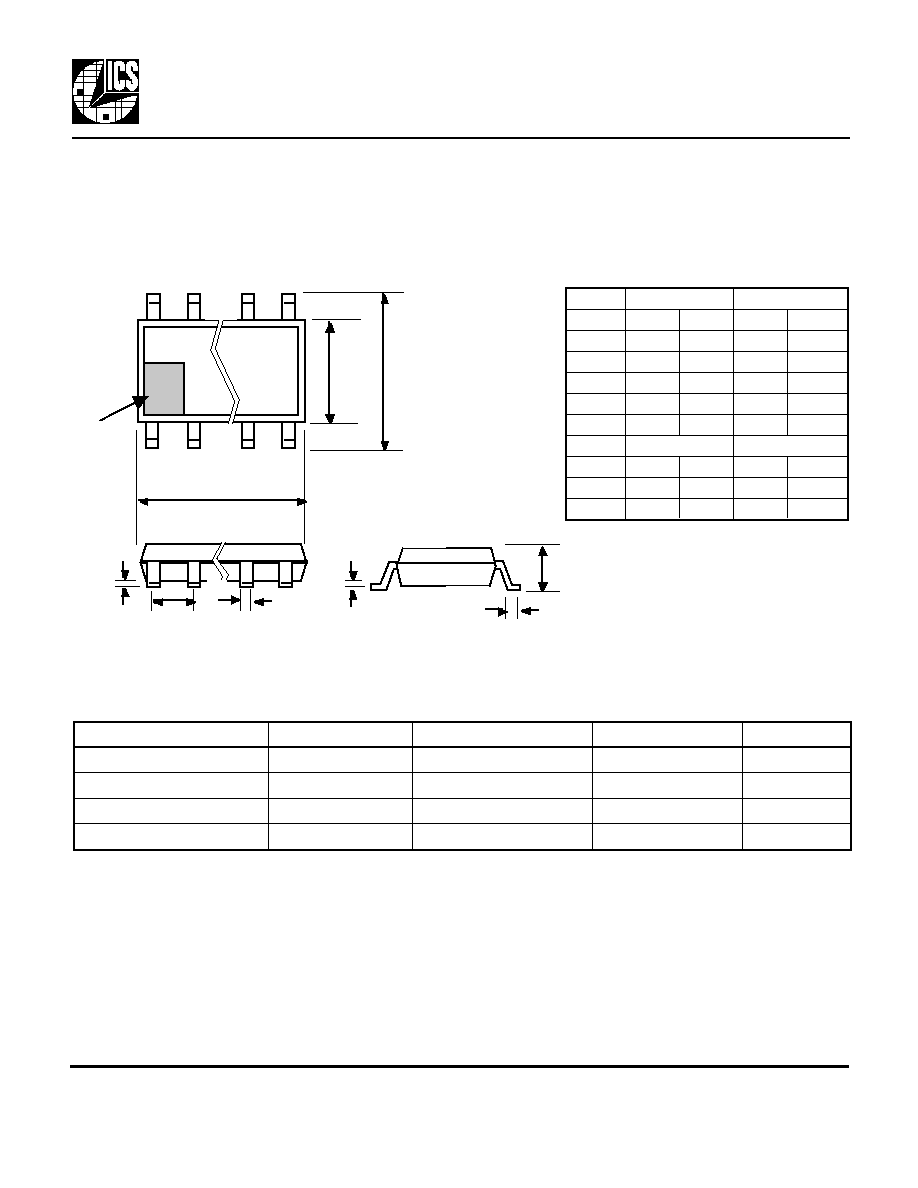
Package Outline and Package Dimensions
(For current dimensional specifications, see JEDEC Publication No. 95.)
2 0 p i n S S O P
Inches
Inches
Millimeters
Millimeters
Symbol
Min
Max
Min
Max
A
0.053
0.069
1.35
1.75
A1
0.004
0.010
0.10
0.25
b
0.008
0.012
0.20
0.30
c
0.007
0.010
0.19
0.25
D
0.337
0.344
8.56
8.74
e .025 BSC
.025 BSC 0.635 BSC
0.635 BSC
E
0.228
0.244
5.79
6.20
E1
0.150
0.157
3.81
3.99
L
0.016
0.050
0.41
1.27
b
D
E1
E
e
A1
c
A
L
INDEX
AREA
1
2