 | –≠–ª–µ–∫—Ç—Ä–æ–Ω–Ω—ã–π –∫–æ–º–ø–æ–Ω–µ–Ω—Ç: V386GLFT | –°–∫–∞—á–∞—Ç—å:  PDF PDF  ZIP ZIP |

V386
V386 Datasheet
1
5/25/05
Revision 2.0
Integrated Circuit Systems ∑ 525 Race Street, San Jose, CA 95126 ∑ tel (408) 297-1201 ∑ www.icst.com
8-B
IT
LVDS R
ECEIVER
FOR
V
IDEO
General Description
The V386 is an ideal LVDS receiver that converts 4-pair
LVDS data streams into parallel 28 bits of CMOS/TTL
data with bandwidth up to 2.38 Gbps throughput or
297.5 Mbytes per second.
This chip is an ideal means to solve EMI and cable size
problems associated with wide, high-speed TTL
interfaces through very low-swing LVDS signals.
ICS manufactures a large variety of video application
devices. Consult ICS for all of your video application
requirements.
Pin Assignments
Features
∑
Pin and function compatible with the National
DS90CF386, THine THC63LVDF84, TI
SN65LVDS94
∑
Converts 4-pair LVDS data streams into parallel 28
bits of CMOS/TTL data
∑
Fully spread spectrum compatible
∑
Wide clock frequency range from 20 MHz to 85 MHz
∑
Supports VGA, SVGA, XGA, and SXGA
∑
LVDS voltage swing of 350 mV for low EMI
∑
On-chip PLL requires no external components
∑
Low-power CMOS design
∑
Falling edge clock triggered outputs
∑
Power-down control function
∑
Compatible with TIA/EIA-644 LVDS standards
∑
Packaged in a 56-pin TSSOP (Pb free available)
Block Diagram
12
1
11
2
10
RxOUT22
3
9
RxOUT23
4
5
6
7
8
16
15
14
13
56-pin TSSOP
17
18
19
20
21
22
23
24
25
26
27
28
29
30
31
32
33
34
35
36
37
38
39
40
41
42
43
44
45
46
47
48
RxOUT24
GND
RxOUT26
RxOUT27
RxOUT25
RxIN0-
RxIN0+
RxIN1-
RxIN1+
LVDS_VCC
LVDS_GND
RxIN2-
RxIN2+
RxCLKIN-
RxCLKIN+
LVDS_GND
PLL_GND
PLL_VCC
PLL_GND
RxOUT2
RxOUT1
VCC
RxOUT8
RxOUT12
VCC
RxOUT3
RxOUT4
RxOUT5
GND
RxOUT6
RxOUT7
RxOUT9
GND
RxOUT10
RxOUT11
VCC
RxOUT13
GND
RxOUT14
RxOUT15
RxOUT16
VCC
V386
PWRDWN
RxCLKOUT
RxOUT0
49
50
51
52
53
54
55
56
LVDS_GND
RxIN3-
RxIN3+
GND
RxOUT17
RxOUT18
RxOUT19
RxOUT20
RxOUT21
RxIN0-
RxIN0+
RxIN1-
RxIN1+
RxIN2-
RxIN2+
RxCLKIN-
RxCLKIN+
RxIN3-
RxIN3+
LVDS to TTL
De-serializer
RED
PLL
GREEN
BLUE
VSYNC
RxCLKOUT
PWRDWN
HSYNC
DATA ENABLE
CONTROL
8
8
8
V386
Rx
O
U
T
0
.
.
2
7

8-B
IT
LVDS R
ECEIVER
FOR
V
IDEO
V386
V386 Datasheet
2
5/25/05
Revision 2.0
Integrated Circuit Systems ∑ 525 Race Street, San Jose, CA 95126 ∑ tel (408) 297-1201 ∑ www.icst.com
Pin Descriptions
Pin
Pin name
Type
Description
1
RxOUT22
OUT
Data outputs on pins (RxOUT0..27)
2
RxOUT23
OUT
Data outputs on pins (RxOUT0..27)
3
RxOUT24
OUT
Data outputs on pins (RxOUT0..27)
4
GND
Ground
Digital ground
5
RxOUT25
OUT
Data outputs on pins (RxOUT0..27)
6
RxOUT26
OUT
Data outputs on pins (RxOUT0..27)
7
RxOUT27
OUT
Data outputs on pins (RxOUT0..27)
8
LVDS_GND
Ground
Analog ground
9
RxIN0-
LVDS IN
LVDS input (-)
10
RxIN0+
LVDS IN
LVDS input (+)
11
RxIN1-
LVDS IN
LVDS input (-)
12
RxIN1+
LVDS IN
LVDS input (+)
13
LVDS_VCC
Power
Analog power
14
LVDS_GND
Ground
Analog ground
15
RxIN2-
LVDS IN
LVDS input (-)
16
RxIN2+
LVDS IN
LVDS input (+)
17
RxCLKIN-
LVDS IN
LVDS input (-)
18
RxCLKIN+
LVDS IN
LVDS input (+)
19
RxIN3-
LVDS IN
LVDS input (-)
20
RxIN3+
LVDS IN
LVDS input (+)
21
LVDS_GND
Ground
Analog ground
22
PLL_GND
Ground
PLL ground
23
PLL_VCC
Power
PLL power
24
PLL_GND
Ground
PLL ground
25
PWRDWN
IN
Power-down control input.
H: Nomal
L: Power down, all ouputs are pulled low.
26
RxCLKOUT
OUT
Clock output
27
RxOUT0
OUT
Data outputs on pins (RxOUT0..27)
28
GND
Ground
Digital ground
29
RxOUT1
OUT
Data outputs on pins (RxOUT0..27)
30
RxOUT2
OUT
Data outputs on pins (RxOUT0..27)
31
VCC
Power
Digital power
32
RxOUT3
OUT
Data outputs on pins (RxOUT0..27)
33
RxOUT4
OUT
Data outputs on pins (RxOUT0..27)
8-B
IT
LVDS R
ECEIVER
FOR
V
IDEO
V386
V386 Datasheet
3
5/25/05
Revision 2.0
Integrated Circuit Systems ∑ 525 Race Street, San Jose, CA 95126 ∑ tel (408) 297-1201 ∑ www.icst.com
.
34
RxOUT5
OUT
Data outputs on pins (RxOUT0..27)
35
RxOUT6
OUT
Data outputs on pins (RxOUT0..27)
36
GND
Ground
Digital ground
37
RxOUT7
OUT
Data outputs on pins (RxOUT0..27)
38
RxOUT8
OUT
Data outputs on pins (RxOUT0..27)
39
RxOUT9
OUT
Data outputs on pins (RxOUT0..27)
40
VCC
Power
Digital power
41
RxOUT10
OUT
Data outputs on pins (RxOUT0..27)
42
RxOUT11
OUT
Data outputs on pins (RxOUT0..27)
43
RxOUT12
OUT
Data outputs on pins (RxOUT0..27)
44
GND
Ground
Digital ground
45
RxOUT13
OUT
Data outputs on pins (RxOUT0..27)
46
RxOUT14
OUT
Data outputs on pins (RxOUT0..27)
47
RxOUT15
OUT
Data outputs on pins (RxOUT0..27)
48
VCC
Power
Digital power
49
RxOUT16
OUT
Data outputs on pins (RxOUT0..27)
50
RxOUT17
OUT
Data outputs on pins (RxOUT0..27)
51
RxOUT18
OUT
Data outputs on pins (RxOUT0..27)
52
GND
Ground
Digital ground
53
RxOUT19
OUT
Data outputs on pins (RxOUT0..27)
54
RxOUT20
OUT
Data outputs on pins (RxOUT0..27)
55
RxOUT21
OUT
Data outputs on pins (RxOUT0..27)
56
VCC
Power
Digital power
Pin
Pin name
Type
Description

8-B
IT
LVDS R
ECEIVER
FOR
V
IDEO
V386
V386 Datasheet
4
5/25/05
Revision 2.0
Integrated Circuit Systems ∑ 525 Race Street, San Jose, CA 95126 ∑ tel (408) 297-1201 ∑ www.icst.com
Absolute Maximum Ratings
Stresses above the ratings listed below can cause permanent damage to the V386. These ratings, which are
standard values for ICS commercially rated parts, are stress ratings only. Functional operation of the device at
these or any other conditions above those indicated in the operational sections of the specifications is not implied.
Exposure to absolute maximum rating conditions for extended periods can affect product reliability. Electrical
parameters are guaranteed only over the recommended operating temperature range.
Recommended Operation Conditions
Electrical Characteristics
VDD=3.3 V ±10%,
Ambient temperature 0 to 70
∞C
Item
Rating
Supply Voltage, VCC
-0.3 V to +4 V
CMOS/TTL Output Voltage
-0.3 V to (VCC+0.3 V)
LVDS Receiver Input Voltage
-0.3 V to (VCC+0.3 V)
Ambient Operating Temperature
0 to +70
∞C
Storage Temperature
-65 to +150
∞C
Junction Temperature
150
∞C
Soldering Temperature (10 seconds max.)
260
∞C
Maximum Package Power
1.61 W (V386)
Package Derating
12.4 mW/∞C above +25∞C
15 mW/∞C above +25∞C
Parameter
Min.
Typ.
Max.
Units
Ambient Operating Temperature (Ta)
0
25
70
∞C
3.3 V Supply Voltage (VCC)
3
3.3
3.6
V
Receiver Input Range (V
IN
)
0
2.4
V
Supply Noise Voltage (V
N
)
100
mVpp
Parameter
Symbol
Conditions
Min.
Typ.
Max.
Units
CMOS/TTL DC Specifications
Input High Voltage
V
IH
2.0
VCC
V
Input Low Voltage
V
IL
GND
0.8
V
Output High Voltage
V
OH
I
OH
= -0.4 mA
2.7
3.3
VCC
V
Output Low Voltage
V
OL
I
OL
= 2 mA
0.06
0.3
V
Input Clamp Voltage
V
CL
I
CL
= -18mA
-0.79
-1.5
V
Input Current
I
IN
VCC
±15
µA

8-B
IT
LVDS R
ECEIVER
FOR
V
IDEO
V386
V386 Datasheet
5
5/25/05
Revision 2.0
Integrated Circuit Systems ∑ 525 Race Street, San Jose, CA 95126 ∑ tel (408) 297-1201 ∑ www.icst.com
0V
±10
Output Short Circuit Current
I
OS
V
OUT
= 0V
-60
mA
LVDS Receiver DC Specifications
Differential Input High Threshold
V
TH
V
CM
= +1.2 V
+100
mV
Differential Input Low Threshold
V
TL
-100
mV
Input Current
I
IN
V
IN
= +2.4 V, VCC = 3.6 V
±10
µA
V
IN
= 0V, VCC = 3.6 V
±15
µA
Receiver Supply Current
Receiver Supply Current (worst case)
I
CCRW
C
L
= 8 pF, f = 65 MHz, worst
case pattern
220
mA
C
L
= 8 pF, f = 85 MHz, worst
case pattern
240
mA
Receiver Supply Current (16
Grayscale)
I
CCRG
C
L
= 8 pF, f = 65 MHz, 16
Grayscale pattern
125
mA
C
L
= 8 pF, f = 85 MHz, 16
Grayscale pattern
140
mA
Receiver Supply Current (Power
Down)
I
CCRZ
Power_Down = Low,
Receiver outputs stay low
during Power-down mode
140
400
µA
Receiver Switching Characteristics
CMOS/TTL Low-to-High Transition
Time
CLHT
20% to 80% VCC, C
L
= 8 pF
2
3.5
ns
CMOS/TTL High-to-Low Transition
Time
CHLT
80% to 20% VCC, C
L
= 8 pF
1.8
3.5
ns
CLKOUT period
RCOP
11.76
T
50
ns
CLKOUT High Time
RCOH
f = 85 MHz
4.5
5
7
ns
CLKOUT Low Time
RCOL
f = 85 MHz
4
5
6.5
ns
Data Setup to CLKOUT
RSRC
f = 85 MHz
2.0
ns
Data Hold to CLKOUT
RHRC
f = 85 MHz
3.5
ns
RCK+/- to CLKOUT Delay
RCCD
25
∞C / 3.3 V
8
14
20
ns
Receiver PLL Setup Time
RPLLS
10
ms
Receiver Power Down Delay
RPDD
1
µs
Receiver Input Strobe Position for
Bit0
RSPos0 f = 85 MHz, T = 11.76 ns
0.49
0.84
1.19
ns
Receiver Input Strobe Position for
Bit1
RSPos1 f = 85 MHz, T = 11.76 ns
2.17
2.52
2.87
ns
Receiver Input Strobe Position for
Bit2
RSPos2 f = 85 MHz, T = 11.76 ns
3.85
4.2
4.55
ns
Receiver Input Strobe Position for
Bit3
RSPos3 f = 85 MHz, T = 11.76 ns
5.53
5.88
6.23
ns
Receiver Input Strobe Position for
Bit4
RSPos4 f = 85 MHz, T = 11.76 ns
7.21
7.56
7.91
ns
Parameter
Symbol
Conditions
Min.
Typ.
Max.
Units

8-B
IT
LVDS R
ECEIVER
FOR
V
IDEO
V386
V386 Datasheet
6
5/25/05
Revision 2.0
Integrated Circuit Systems ∑ 525 Race Street, San Jose, CA 95126 ∑ tel (408) 297-1201 ∑ www.icst.com
Note: The skew margins mean the maximum timing tolerance between the clock and data channel when the
receiver still works well. This margin takes into acount the receiver input setup and hold time, and internal clock
jitter (i.e., internal data sampling window - RSPos). Thyis margin allows for LVDS transmitter pulse position,
interconnect skew, inter-symbol interference and intrinsic channel mismatch which will cause the skew between
clock (RC+ and RCK-) and data (RX[n]+ and RX[n]- ; n =0, 1, 2, 3) channels.
Thermal Characteristics
Receiver Input Strobe Position for
Bit5
RSPos5 f = 85 MHz, T = 11.76 ns
8.89
9.24
9.59
ns
Receiver Input Strobe Position for
Bit6
RSPos6 f = 85 MHz, T = 11.76 ns
10.57
10.92
11.27
ns
RxIn Skew Margin (see note and
Figure 8)
Rskm
f = 85 MHz, T = 11.76 ns
300
ps
f = 65 MHz, T = 15.38 ns
500
ps
Parameter
Symbol
Conditions
Min.
Typ.
Max.
Units
Thermal Resistance Junction to Ambient
JA
Still air
84
∞C/W
JA
1 m/s air flow
76
∞C/W
JA
3 m/s air flow
67
∞C/W
Thermal Resistance Junction to Case
JC
50
∞C/W
Parameter
Symbol
Conditions
Min.
Typ.
Max.
Units

8-B
IT
LVDS R
ECEIVER
FOR
V
IDEO
V386
V386 Datasheet
7
5/25/05
Revision 2.0
Integrated Circuit Systems ∑ 525 Race Street, San Jose, CA 95126 ∑ tel (408) 297-1201 ∑ www.icst.com
Timing Diagrams
Figure 1a. "Worst Case" Test Pattern
Figure 1b. 16-Grayscale Test-Pattern Waveforms
Figure 2. V386 CMOS/TTL Output Load and Transition Time
CLKIN/CLKOUT
T
ODD Data In/Data Out
EVEN Data In/Data Out
CLKOUT
D0, 8, 16
D1, 9, 17
D2, 10, 18
D3, 11, 19
D4-7, 12-15, 20-23
D24-27
V386 CMO/TTL Output Load and Transition Times
20%
20%
80%
80%
CLHT
CHLT
CMOS/TTL Output
8pF

8-B
IT
LVDS R
ECEIVER
FOR
V
IDEO
V386
V386 Datasheet
8
5/25/05
Revision 2.0
Integrated Circuit Systems ∑ 525 Race Street, San Jose, CA 95126 ∑ tel (408) 297-1201 ∑ www.icst.com
Figure 3. V386 SETUP/HOLD and High/Low Times
Figure 4. V386 Clock In to Clock Out Delay
Figure 5. V386 Phase Lock Loop Set Time
Figure 6. V386 Power Down Delay
CLKOUT
D0 ≠ D27 Out
0.8 V
2.0 V
RCOP
2.0 V
2.0 V
0.8 V
RCOH
RCOL
RSRC
RHRC
2.0 V
SETUP
2.0 V
HOLD
CLKOUT
Vdiff=0V
RCCD
RCK
1.5V
CLKOUT
RPLLS
RCK
3.0 V
2.0 V
3.6 V
VCC
PWRDWN
RPDD
1.5 V
PWRDWN
RCK IN
Low

8-B
IT
LVDS R
ECEIVER
FOR
V
IDEO
V386
V386 Datasheet
9
5/25/05
Revision 2.0
Integrated Circuit Systems ∑ 525 Race Street, San Jose, CA 95126 ∑ tel (408) 297-1201 ∑ www.icst.com
Figure 7. V386 LVDS Input Strobe Position
Figure 8. Receiver Input Skew Margin
Rspos0 Min
Previous Cycle
Rspos0 Max
Rspos1 Min
Rspos1 Max
Rspos2 Min
Rspos3 Min
Rspos2 Max
Rspos3 Max
Rspos4 Min
Rspos4 Max
Rspos5 Min
Rspos5 Max
Rspos6 Min
Rspos6 Max
Next Cycle
TCLK
Data
Clock
RCK+/RCK-
RX[n]+/RX[n]-
N = 0, 1, 2, 3
Skew Margin
8-B
IT
LVDS R
ECEIVER
FOR
V
IDEO
V386
V386 Datasheet
10
5/25/05
Revision 2.0
Integrated Circuit Systems ∑ 525 Race Street, San Jose, CA 95126 ∑ tel (408) 297-1201 ∑ www.icst.com
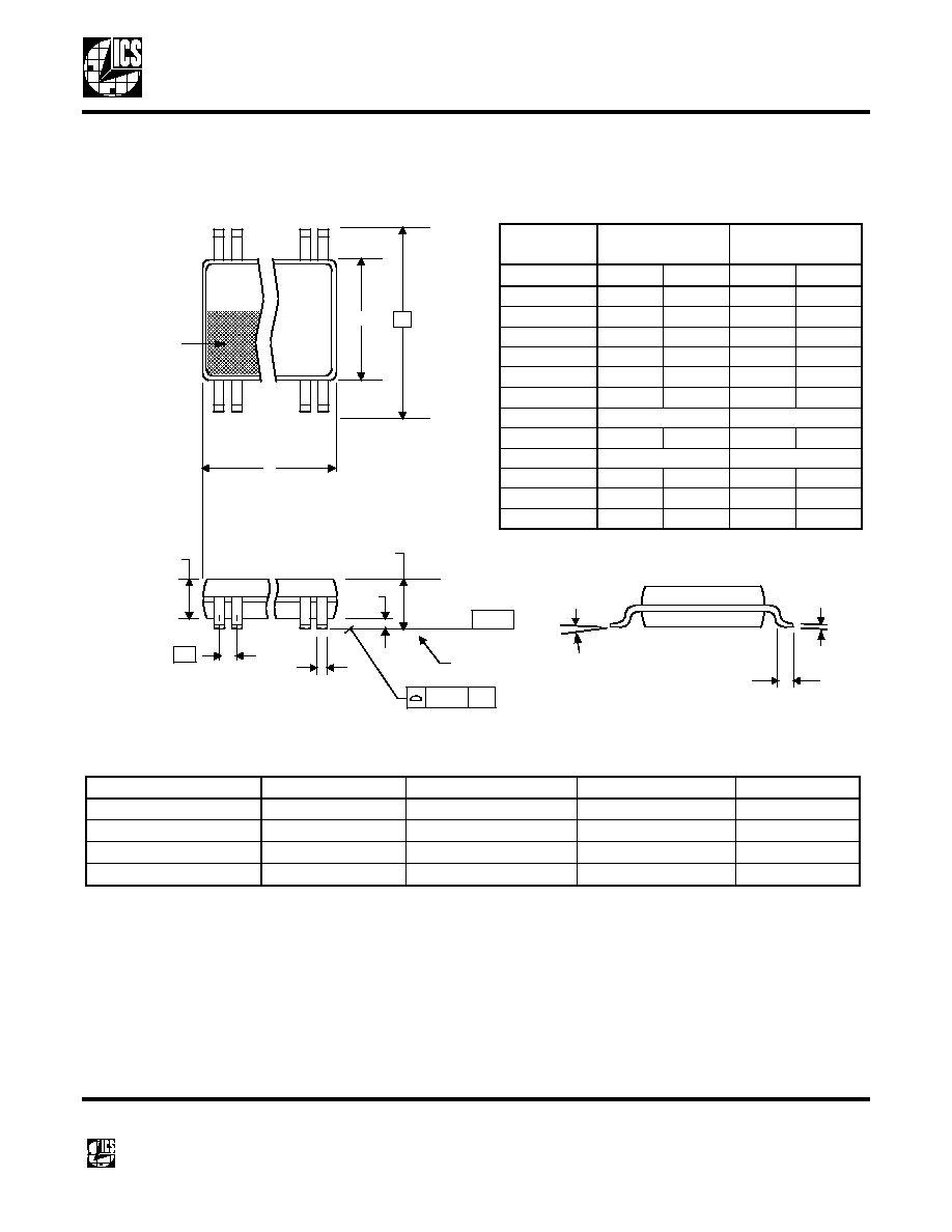
Package Outline and Package Dimensions
(56-pin TSSOP)
Package dimensions are kept current with JEDEC Publication No. 95
Ordering Information
Parts that are ordered with a "LF" suffix to the part number are the Pb-Free configuration and are RoHS compliant.
While the information presented herein has been checked for both accuracy and reliability, Integrated Circuit
Systems (ICS) assumes no responsibility for either its use or for the infringement of any patents or other rights of
third parties, which would result from its use. No other circuits, patents, or licenses are implied. This product is
intended for use in normal commercial applications. Any other applications such as those requiring extended
temperature range, high reliability, or other extraordinary environmental requirements are not recommended
without additional processing by ICS. ICS reserves the right to change any circuitry or specifications without notice.
ICS does not authorize or warrant any ICS product for use in life support devices or critical medical instruments.
Part / Order Number
Marking
Shipping Packaging
Package
Temperature
V386G
V386G
Tubes
56-pin TSSOP
0 to +70
∞C
V386GT
V386G
Tape and Reel
56-pin TSSOP
0 to +70
∞C
V386GLF
V386GLF
Tubes
56-pin TSSOP
0 to +70
∞C
V386GLFT
V386GLF
Tape and Reel
56-pin TSSOP
0 to +70
∞C
INDEX
AREA
1 2
56
D
E1
E
SEATING
PLANE
A
1
A
A
2
e
- C -
b
aaa
C
c
L
Millimeters
Inches*
Symbol
Min
Max
Min
Max
A
--
1.20
--
0.047
A1
0.05
0.15
0.002
0.006
A2
0.80
1.05
0.032
0.041
b
0.17
0.27
0.007
0.011
C
0.09
0.20
0.0035
0.008
D
13.90
14.10
0.547
0.555
E
8.10 BASIC
0.319 BASIC
E1
6.00
6.20
0.236
0.244
e
0.50 BASIC
0.020 BASIC
L
0.45
0.75
0.018
0.030
a
0
∞
8
∞
0
∞
8
∞
aaa
--
0.10
--
0.004
* For reference only. Controlling dimensions in mm.