 | –≠–ª–µ–∫—Ç—Ä–æ–Ω–Ω—ã–π –∫–æ–º–ø–æ–Ω–µ–Ω—Ç: 5T2010 | –°–∫–∞—á–∞—Ç—å:  PDF PDF  ZIP ZIP |
1
INDUSTRIAL TEMPERATURE RANGE
IDT5T2010
2.5V ZERO DELAY PLL CLOCK DRIVER TERACLOCK
1sOE
2sOE
1
Q
0
1
Q
1
2
Q
0
2
Q
1
3
Q
0
3
Q
1
4
Q
0
4
Q
1
5
Q
0
5
Q
1
Q
FB
Q
FB
Divide
Select
1F
2:1
Divide
Select
2F
2:1
Divide
Select
3F
2:1
Divide
Select
4F
2:1
Divide
Select
5F
2:1
TxS
REF
0
REF
0
/
V
REF0
FB
FB/
V
REF2
RxS
REF
1
REF
1
/
V
REF1
0
1
PLL
PD
FS
LOCK
PE
PLL_EN
/N
DS
1:0
3
3
REF_SEL
0
1
Divide
Select
FBF
2:1
OMODE
3sOE
4sOE
5sOE
MAY 2003
2003 Integrated Device Technology, Inc.
DSC 5981/21
c
INDUSTRIAL TEMPERATURE RANGE
The IDT logo is a registered trademark of Integrated Device Technology, Inc.
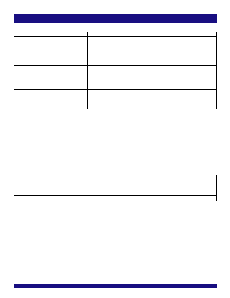
FEATURES:
∑ 2.5 V
DD
∑ 5 pairs of outputs
∑ Low skew: 50ps same pair, 100ps all outputs
∑ Selectable positive or negative edge synchronization
∑ Tolerant of spread spectrum input clock
∑ Synchronous output enable
∑ Selectable inputs
∑ Input frequency: 4.17MHz to 250MHz
∑ Output frequency: 12.5MHz to 250MHz
∑ 1.8V / 2.5V LVTTL: up to 250MHz
∑ HSTL / eHSTL: up to 250MHz
∑ Hot insertable and over-voltage tolerant inputs
∑ 3-level inputs for selectable interface
∑ 3-level inputs for feedback divide selection with multiply ratios
of(1-6, 8, 10, 12)
∑ Selectable HSTL, eHSTL, 1.8V/2.5V LVTTL, or LVEPECL input
interface
∑ Selectable differential or single-ended inputs and ten single-
ended outputs
∑ PLL bypass for DC testing
∑ External differential feedback, internal loop filter
∑ Low Jitter: <75ps cycle-to-cycle
∑ Power-down mode
∑ Lock indicator
∑ Available in BGA and MLF packages
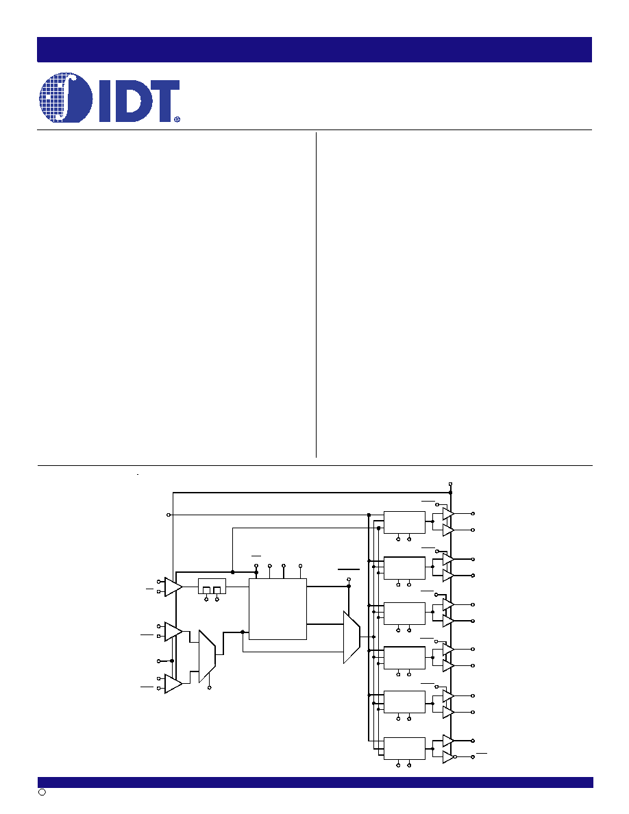
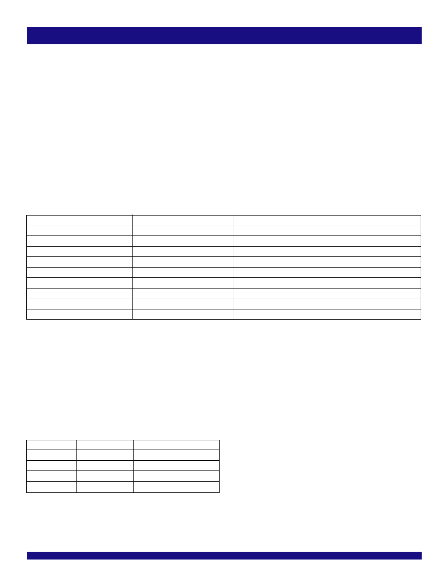
FUNCTIONAL BLOCK DIAGRAM
IDT5T2010
PRELIMINARY
2.5V ZERO DELAY PLL
CLOCK DRIVER TERACLOCKTM
DESCRIPTION:
The IDT5T2010 is a 2.5V PLL clock driver intended for high perfor-
mance computing and data-communications applications. The IDT5T2010
has ten outputs in five banks of two, plus a dedicated differential feedback.
The redundant input capability allows for a smooth change over to a
secondary clock source when the primary clock source is absent.
The feedback bank allows divide-by-functionality from 1 to 12 through
the use of the DS[1:0] inputs. This provides the user with frequency
multiplication 1 to 12 without using divided outputs for feedback. Each output
bank also allows for a divide-by functionality of 2 or 4.
The IDT5T2010 features a user-selectable, single-ended or differential
input to ten single-ended outputs. The clock driver also acts as a translator from
a differential HSTL, eHSTL, 1.8V/2.5V LVTTL, LVEPECL, or single-ended
1.8V/2.5V LVTTL input to HSTL, eHSTL, or 1.8V/2.5V LVTTL outputs.
Selectable interface is controlled by 3-level input signals that may be hard-wired
to appropriate high-mid-low levels. The outputs can be synchronously
enabled/disabled.
Furthermore, when PE is held high, all the outputs are synchronized with
the positive edge of the REF clock input. When PE is held low, all the outputs
are synchronized with the negative edge of REF.
2
INDUSTRIAL TEMPERATURE RANGE
IDT5T2010
2.5V ZERO DELAY PLL CLOCK DRIVER TERACLOCK
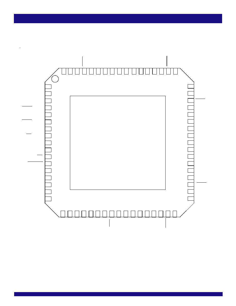
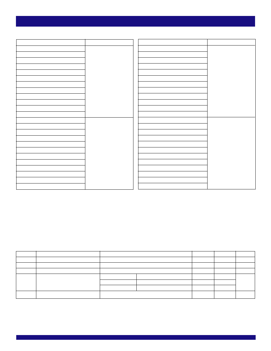
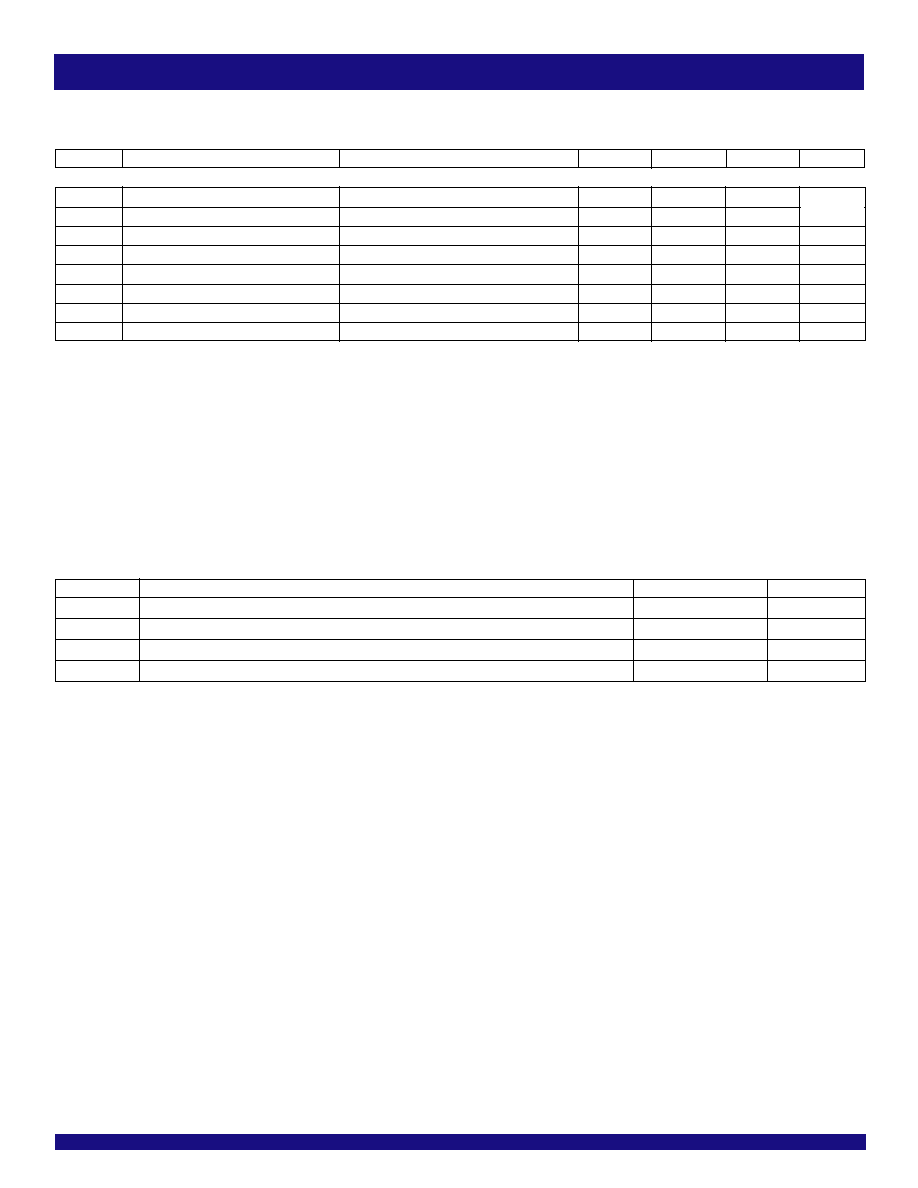
PIN CONFIGURATION
A
A
1F
2
V
DD
GND
1sOE
1
Q
0
1
Q
1
GND
2
Q
1
2
Q
0
2sOE
2F
2
V
DDQ
B
B
V
DD
V
DD
1F
1
GND
GND
2F
1
V
DD
NC
NC
V
DDQ
V
DDQ
3F
2
C
C
V
DD
OMODE
V
DD
V
DD
GND
GND
GND
GND
V
DDQ
V
DDQ
D
E
F
G
H
J
K
L
M
D
E
F
G
H
J
K
L
M
1
2
3
4
5
6
7
8
9
10
11
12
1
2
REF
1
/V
REF1
REF
0
/V
REF0
FB
/V
REF2
PLL_
EN
GND
TxS
V
DD
V
DD
DS
0
3
4
5
6
7
8
9
10
11
12
REF_
SEL
REF
1
PD
RxS
LOCK
V
DD
DS
1
FB
REF
0
NC
3F
1
V
DDQ
V
DDQ
4F
1
NC
3
Q
0
3
Q
1
V
DDQ
V
DDQ
4
Q
1
4
Q
0
FBF
1
GND
GND
5F
1
FS
FBF
2
V
DD
NC
V
DD
V
DD
PE
V
DD
V
DD
V
DD
V
DD
V
DD
V
DD
V
DD
V
DD
V
DD
NC
QFB
QFB
GND
GND
5
Q
1
5
Q
0
NC
GND
GND
GND
GND
GND
GND
GND
GND
GND
GND
GND
GND
GND
GND
GND
GND
GND
GND
GND
GND
GND
GND
GND
GND
GND
GND
GND
V
DDQ
V
DDQ
V
DDQ
V
DDQ
V
DDQ
V
DDQ
V
DDQ
V
DDQ
V
DDQ
V
DDQ
5F
2
4F
2
V
DDQ
GND
V
DDQ
V
DDQ
V
DDQ
V
DDQ
V
DDQ
V
DDQ
V
DDQ
V
DDQ
3sOE
4sOE
5sOE
BGA
TOP VIEW
3
INDUSTRIAL TEMPERATURE RANGE
IDT5T2010
2.5V ZERO DELAY PLL CLOCK DRIVER TERACLOCK
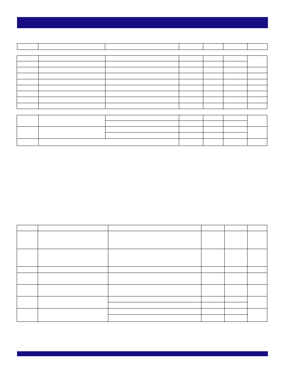
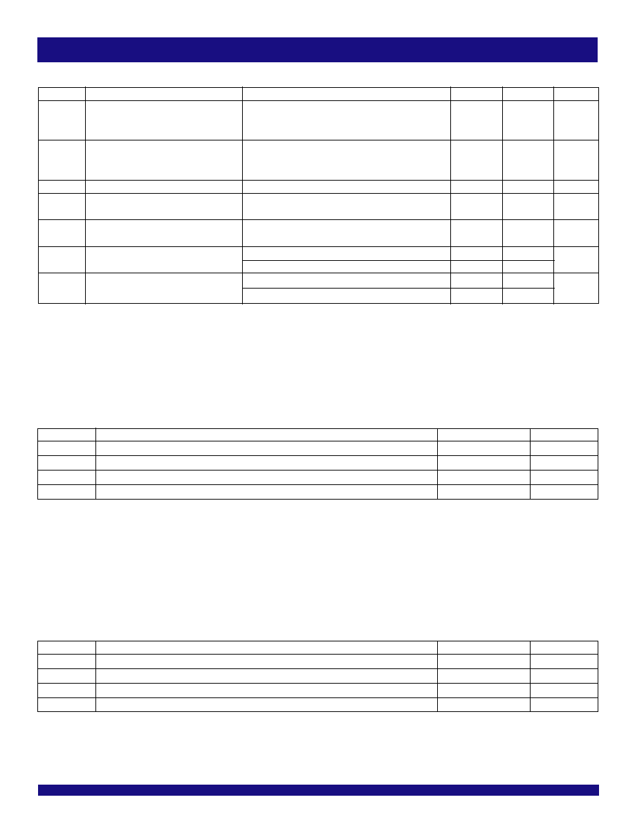
PIN CONFIGURATION
MLF
TOP VIEW
2
F
1
V
D
D
Q
V
D
D
1
F
1
1
F
2
1
Q
1
1
s
O
E
V
D
D
O
M
O
D
E
6
8
6
7
6
6
6
5
6
4
6
3
6
2
6
1
6
0
5
9
V
D
D
Q
2
F
2
2
Q
0
2
s
O
E
V
D
D
Q
V
D
D
Q
2
Q
1
5
8
5
7
5
6
5
5
5
4
5
3
5
2
1
Q
0
2
0
2
1
2
2
2
3
2
4
2
5
2
6
2
7
V
D
D
Q
F
S
F
B
F
2
Q
F
B
F
B
F
1
V
D
D
Q
Q
F
B
V
D
D
1
8
1
9
D
S
1
D
S
0
2
8
2
9
3
0
3
1
3
2
3
3
3
4
5
Q
0
5
F
1
5
Q
1
5
s
O
E
5
F
2
V
D
D
Q
V
D
D
Q
3
sOE
3
F
2
V
DDQ
V
DDQ
3
Q
0
51
50
49
48
47
46
45
44
43
42
3
Q
1
V
DD
4
F
1
V
DD
3
F
1
4
Q
1
4
Q
0
V
DDQ
41
40
39
38
37
36
35
V
DDQ
4
F
2
V
DD
4
sOE
REF_SEL
V
DD
REF
1
FB
REF
1
/V
REF1
REF
0
REF
0
/V
REF0
2
3
4
5
6
7
1
PE
FB/V
REF2
8
9
10
V
DD
PD
PLL_EN
V
DD
V
DD
RxS
TxS
LOCK
12
13
14
15
16
17
11
GND
4
INDUSTRIAL TEMPERATURE RANGE
IDT5T2010
2.5V ZERO DELAY PLL CLOCK DRIVER TERACLOCK
NOTE:
1. Capacitance applies to all inputs except RxS, TxS, nF
[2:1]
, FBF
[2:1]
, and DS
[1:0]
.
CAPACITANCE
(T
A
= +25∞C, f = 1MHz, V
IN
= 0V)
Parameter
Description
Min.
Typ.
Max.
Unit
C
IN
Input Capacitance
2.5
3
3.5
pF
C
OUT
Output Capacitance
--
6.3
7
pF
Symbol
Description
Max
Unit
V
DDQ
, V
DD
Power Supply Voltage
(2)
≠0.5 to +3.6
V
V
I
Input Voltage
≠0.5 to +3.6
V
V
O
Output Voltage
≠0.5 to V
DDQ
+0.5
V
V
REF
Reference Voltage
(3)
≠0.5 to +3.6
V
T
J
Junction Temperature
150
∞C
T
STG
Storage Temperature
≠65 to +165
∞C
ABSOLUTE MAXIMUM RATINGS
(1)
NOTES:
1. Stresses greater than those listed under ABSOLUTE MAXIMUM RATINGS may cause
permanent damage to the device. This is a stress rating only and functional operation
of the device at these or any other conditions above those indicated in the operational
sections of this specification is not implied. Exposure to absolute maximum rating
conditions for extended periods may affect reliability.
2. V
DDQ
and V
DD
internally operate independently. No power sequencing requirements
need to be met.
3. Not to exceed 3.6V.
Symbol
Description
Min.
Typ.
Max.
Unit
T
A
Ambient Operating Temperature
≠40
+25
+85
∞C
V
DD
(1)
Internal Power Supply Voltage
2.3
2.5
2.7
V
HSTL Output Power Supply Voltage
1.4
1.5
1.6
V
V
DDQ
(1)
Extended HSTL and 1.8V LVTTL Output Power Supply Voltage
1.65
1.8
1.95
V
2.5V LVTTL Output Power Supply Voltage
V
DD
V
V
T
Termination Voltage
V
DDQ
/ 2
V
RECOMMENDED OPERATING RANGE
NOTE:
1. Inputs are capable of translating the following interface standards. User can select between:
Single-ended 2.5V LVTTL levels
Single-ended 1.8V LVTTL levels
or
Differential 2.5V/1.8V LVTTL levels
Differential HSTL and eHSTL levels
Differential LVEPECL levels
PIN DESCRIPTION
Symbol
I/O
Type
Description
REF
[1:0]
I
Adjustable
(1)
Clock input. REF
[1:0]
is the "true" side of the differential clock input. If operating in single-ended mode, REF
[1:0]
is the clock input.
REF
[1:0]
/
I
Adjustable
(1)
Complementary clock input. REF
[1:0]
/V
REF
[1:0]
is the "complementary" side of REF
[1:0]
if the input is in differential mode. If operating
V
REF
[1:0]
in single-ended mode, REF
[1:0]
/V
REF
[1:0]
is left floating. For single-ended operation in differential mode, REF
[1:0]
/V
REF
[1:0]
should be set
to the desired toggle voltage for REF
[1:0]
:
2.5V LVTTL
V
REF
= 1250mV (SSTL2 compatible)
1.8V LVTTL, eHSTL
V
REF
= 900mV
HSTL
V
REF
= 750mV
LVEPECL
V
REF
= 1082mV
FB
I
Adjustable
(1)
Clock input. FB is the "true" side of the differential feedback clock input. If operating in single-ended mode, FB is the feedback clock input.
FB/V
REF
2
I
Adjustable
(1)
Complementary feedback clock input. FB/V
REF
2
is the "complementary" side of FB if the input is in differential mode. If operating in single-
ended mode, FB/V
REF
2
is left floating. For single-ended operation in differential mode, FB/V
REF
2
should be set to the desired toggle voltage
for FB:
2.5V LVTTL
V
REF
= 1250mV (SSTL2 compatible)
1.8V LVTTL, eHSTL
V
REF
= 900mV
HSTL
V
REF
= 750mV
LVEPECL
V
REF
= 1082mV
NOTE:
1. All power supplies should operate in tandem. If V
DD
or V
DDQ
is at maximum, then V
DDQ
or V
DD
(respectively) should be at maximum, and vice-versa.

5
INDUSTRIAL TEMPERATURE RANGE
IDT5T2010
2.5V ZERO DELAY PLL CLOCK DRIVER TERACLOCK
PIN DESCRIPTION, CONTINUED
Symbol
I/O
Type
Description
REF_SEL
I
LVTTL
(1)
Reference clock select. When LOW, selects REF
0
and REF
0
/V
REF
0.
When HIGH, selects REF
1
and REF
1
/V
REF
1.
nsOE
I
LVTTL
(1)
Synchronous output enable. When nsOE is HIGH, nQ
[1:0]
are synchronously stopped. OMODE selects whether the outputs are gated
LOW/HIGH or tri-stated. When OMODE is HIGH, PE determines the level at which the outputs stop. When PE is LOW/HIGH, the
nQ
[1:0]
is stopped in a HIGH/LOW state. When OMODE is LOW, the outputs are tri-stated. Set nsOE LOW for normal operation.
QFB
O
Adjustable
(2)
Feedback clock output
QFB
O
Adjustable
(2)
Complementary feedback clock output
nQ
[1:0]
O
Adjustable
(2)
Five banks of two outputs
RxS
I
3-Level
(3)
Selects single-ended 2.5V LVTTL (HIGH), 1.8V LVTTL (MID) REF clock input or differential (LOW) REF clock input
TxS
I
3-Level
(3)
Sets the drive strength of the output drivers and feedback inputs to be 2.5V LVTTL (HIGH), 1.8V LVTTL (MID) or HSTL/eHSTL (LOW)
compatible. Used in conjuction with V
DDQ
to set the interface levels.
PE
I
LVTTL
(1)
Selectable positive or negative edge control. When LOW/HIGH the outputs are synchronized with the negative/positive edge of the reference
clock (has internal pull-up).
nF
[2:1]
I
LVTTL
(1)
Function select inputs for divide-by-2, divide-by-4, zero delay, or invert on each bank (See Control Summary table)
FBF
[2:1]
I
LVTTL
(1)
Function select inputs for divide-by-2, divide-by-4, zero delay, or invert on the feedback bank (See Control Summary table)
FS
I
LVTTL
(1)
Selects appropriate oscillator circuit based on anticipated frequency range. (See VCO Frequency Range Select.)
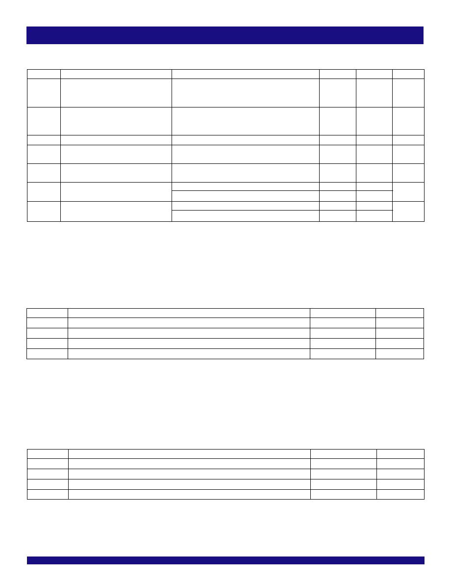
DS
[1:0]
I
3-Level
(3)
3-level inputs for feedback input divider selection (See Divide Selection table)
PLL_EN
I
LVTTL
(1)
PLL enable/disable control. Set LOW for normal operation. When PLL_EN is HIGH, the PLL is disabled and REF
[1:0]
goes to all outputs.
PD
I
LVTTL
(1)
Power down control. When PD is LOW, the inputs are disabled and internal switching is stopped. OMODE selects whether the outputs
are gated LOW/HIGH or tri-stated. When OMODE is HIGH, PE determines the level at which the outputs stop. When PE is LOW/
HIGH, the nQ
[1:0]
and QFB are stopped in a HIGH/LOW state, while the QFB is stopped in a LOW/HIGH state. When OMODE is
LOW, the outputs are tri-stated. Set PD HIGH for normal operation.
LOCK
O
LVTTL
PLL lock indication signal. HIGH indicates lock. LOW indicates that the PLL is not locked and outputs may not be synchronized to the
inputs. The output will be 2.5V LVTTL.
OMODE
I
LVTTL
(1)
Output disable control. Determines the outputs' disable state. Used in conjunction with nsOE and PD. (See Output Enable/Disable and
Powerdown tables.)
V
DDQ
PWR
Power supply for output buffers. When using 2.5V LVTTL, V
DDQ
should be connected to V
DD.
V
DD
PWR
Power supply for phase locked loop, lock output, inputs, and other internal circuitry
GND
PWR
Ground
NOTES:
1. Pins listed as LVTTL inputs will accept 2.5V signals under all conditions. If the output is operating at 1.8V or 1.5V, the LVTTL inputs will accept 1.8V LVTTL signals as well.
2. Outputs are user selectable to drive 2.5V, 1.8V LVTTL, eHSTL, or HSTL interface levels when used with the appropriate V
DDQ
voltage.
3. 3-level inputs are static inputs and must be tied to V
DD
or GND or left floating. These inputs are not hot-insertable or over voltage tolerant.
NOTE:
1. The level to be set on FS is determined by the nominal operating frequency of the
VCO. The VCO frequency (F
NOM
) always appears at nQ
[1:0]
outputs when they are
operated in their undivided modes. The frequency appearing at the REF
[1:0]
and
REF
[1:0]
/V
REF
[1:0]
and FB and FB/V
REF
2 inputs will be F
NOM
when the QFB and QFB
are undivided and DS
[1:0]
= MM. The frequency of REF
[1:0]
and REF
[1:0]
/V
REF
[1:0]
and FB and FB/V
REF
2 inputs will be F
NOM
/2 or F
NOM
/4 when the part is configured for
frequency multiplication by using a divided QFB and QFB and setting DS
[1:0]
= MM.
Using the DS
[1:0]
inputs allows a different method for frequency multiplication (see
Divide Selection table).
VCO FREQUENCY RANGE SELECT
FS
(1)
Min.
Max.
Unit
LOW
50
125
MHz
HIGH
100
250
MHz
NOTE:
1. PE determines the level at which the outputs stop. When PE is LOW/HIGH, the
nQ
[1:0]
is stopped in a HIGH/LOW state.
OUTPUT ENABLE/DISABLE
nsOE
OMODE
Output
L
X
Normal Operation
H
L
Tri-State
H
H
Gated
(1)
NOTE:
1. PE determines the level at which the outputs stop. When PE is LOW/HIGH, the
nQ
[1:0]
and QFB are stopped in a HIGH/LOW state, while the QFB is stopped in a
LOW/HIGH state.
POWERDOWN
PD
OMODE
Output
H
X
Normal Operation
L
L
Tri-State
L
H
Gated
(1)
6
INDUSTRIAL TEMPERATURE RANGE
IDT5T2010
2.5V ZERO DELAY PLL CLOCK DRIVER TERACLOCK
EXTERNAL DIFFERENTIAL FEEDBACK
By providing a dedicated external differential feedback, the IDT5T2010
gives users flexibility with regard to divide selection. The FB and FB/
V
REF2
signals are compared with the input REF
[1:0]
and REF
[1:0]
/V
REF[1:0]
signals at the phase detector in order to drive the VCO. Phase differ-
ences cause the VCO of the PLL to adjust upwards or downwards
accordingly.
An internal loop filter moderates the response of the VCO to the
phase detector. The loop filter transfer function has been chosen to
provide minimal jitter (or frequency variation) while still providing accu-
rate responses to input frequency changes.
DIVIDE SELECTION TABLE
DS [
1:0
]
Divide-by-n
Permitted Output Divide-by-n connected to FB and FB/V
REF2(1)
LL
2
1, 2
LM
3
1
LH
4
1, 2
ML
5
1, 2
M M
1
1, 2, 4
M H
6
1, 2
HL
8
1
H M
10
1
H H
12
1
NOTE:
1. Permissible output division ratios connected to FB and FB/V
REF
2
. The frequencies of the REF
[1:0]
and REF
[1:0]
/V
REF
[1:0]
inputs will be F
NOM
/N when the parts are configured for
frequency multiplication by using an undivided output for FB and FB/V
REF
2
and setting DS[
1:0
] to N (N = 1-6, 8, 10, 12).
CONTROL SUMMARY TABLE FOR ALL
OUTPUTS
nF
2
/FBF
2
nF
1
/FBF
1
Output Skew
L
L
Divide by 2
L
H
Zero Delay
H
L
Inverted
H
H
Divide by 4
7
INDUSTRIAL TEMPERATURE RANGE
IDT5T2010
2.5V ZERO DELAY PLL CLOCK DRIVER TERACLOCK
INPUT/OUTPUT SELECTION
(1)
Input
Output
2.5V LVTTL SE
2.5V LVTTL
1.8V LVTTL SE
2.5V LVTTL DSE
1.8V LVTTL DSE
LVEPECL DSE
eHSTL DSE
HSTL DSE
2.5V LVTTL DIF
1.8V LVTTL DIF
LVEPECL DIF
eHSTL DIF
HSTL DIF
2.5V LVTTL SE
1.8V LVTTL
1.8V LVTTL SE
2.5V LVTTL DSE
1.8V LVTTL DSE
LVEPECL DSE
eHSTL DSE
HSTL DSE
2.5V LVTTL DIF
1.8V LVTTL DIF
LVEPECL DIF
eHSTL DIF
HSTL DIF
Input
Output
2.5V LVTTL SE
eHSTL
1.8V LVTTL SE
2.5V LVTTL DSE
1.8V LVTTL DSE
LVEPECL DSE
eHSTL DSE
HSTL DSE
2.5V LVTTL DIF
1.8V LVTTL DIF
LVEPECL DIF
eHSTL DIF
HSTL DIF
2.5V LVTTL SE
HSTL
1.8V LVTTL SE
2.5V LVTTL DSE
1.8V LVTTL DSE
LVEPECL DSE
eHSTL DSE
HSTL DSE
2.5V LVTTL DIF
1.8V LVTTL DIF
LVEPECL DIF
eHSTL DIF
HSTL DIF
NOTE:
1. The INPUT/OUTPUT SELECTION Table describes the total possible combinations of input and output interfaces. Single-Ended (SE) inputs in a single-ended mode require the
REF
[1:0]
/V
REF
[1:0]
and FB/V
REF
2
pins to be left floating. Differential Single-Ended (DSE) is for single-ended operation in differential mode, requiring V
REF
[1:0]
and V
REF
2
. Differential
(DIF) inputs are used only in differential mode.
NOTE:
1. These inputs are normally wired to V
DD
, GND, or left floating. Internal termination resistors bias unconnected inputs to V
DD
/2. If these inputs are switched dynamically after powerup,
the function and timing of the outputs may be glitched, and the PLL may require additional t
LOCK
time before all datasheet limits are achieved.
DC ELECTRICAL CHARACTERISTICS OVER OPERATING RANGE
Symbol
Parameter
Test Conditions
Min.
Max
Unit
V
IHH
Input HIGH Voltage Level
(1)
3-Level Inputs Only
V
DD
≠ 0.4
--
V
V
IMM
Input MID Voltage Level
(1)
3-Level Inputs Only
V
DD
/2 ≠ 0.2 V
DD
/2 + 0.2
V
V
ILL
Input LOW Voltage Level
(1)
3-Level Inputs Only
--
0.4
V
V
IN
= V
DD
HIGH Level
--
200
I
3
3-Level Input DC Current
V
IN
= V
DD
/2
MID Level
≠50
+50
µA
(RxS, TxS, DS
[1:0]
)
V
IN
= GND
LOW Level
≠200
--
I
PU
Input Pull-Up Current (PE)
V
DD
= Max., V
IN
= GND
≠100
--
µA
8
INDUSTRIAL TEMPERATURE RANGE
IDT5T2010
2.5V ZERO DELAY PLL CLOCK DRIVER TERACLOCK
DC ELECTRICAL CHARACTERISTICS OVER OPERATING RANGE FOR HSTL
(1)
Symbol
Parameter
Test Conditions
Min.
Typ.
(7)
Max
Unit
Input Characteristics
I
IH
Input HIGH Current
V
DD
= 2.7V
V
I
= V
DDQ
/GND
--
--
±5
µA
I
IL
Input LOW Current
V
DD
= 2.7V
V
I
= GND/V
DDQ
--
--
±5
V
IK
Clamp Diode Voltage
V
DD
= 2.3V, I
IN
= -18mA
--
- 0.7
- 1.2
V
V
IN
DC Input Voltage
- 0.3
+3.6
V
V
DIF
DC Differential Voltage
(2,8)
0.2
--
V
V
CM
DC Common Mode Input Voltage
(3,8)
680
750
900
mV
V
IH
DC Input HIGH
(4,5,8)
V
REF
+ 100
--
mV
V
IL
DC Input LOW
(4,6,8)
--
V
REF
- 100
mV
V
REF
Single-Ended Reference Voltage
(4,8)
--
750
--
mV
Output Characteristics
V
OH
Output HIGH Voltage
I
OH
= -8mA
V
DDQ
- 0.4
--
V
I
OH
= -100
µA
V
DDQ
- 0.1
--
V
OL
Output LOW Voltage
I
OL
= 8mA
--
0.4
V
I
OL
= 100
µA
--
0.1
V
OX
FB/FB Output Crossing Point
V
DDQ
/2 - 150
V
DDQ
/2
V
DDQ
/2 + 150
mV
NOTES:
1. See RECOMMENDED OPERATING RANGE table.
2. V
DIF
specifies the minimum input differential voltage (V
TR
- V
CP
) required for switching where V
TR
is the "true" input level and V
CP
is the "complement" input level. Differential mode
only. The DC differential voltage must be maintained to guarantee retaining the existing HIGH or LOW input. The AC differential voltage must be achieved to guarantee switching
to a new state.
3. V
CM
specifies the maximum allowable range of (V
TR
+ V
CP
) /2. Differential mode only.
4. For single-ended operation, in differential mode, REF
[1:0]
/V
REF
[1:0]
is tied to the DC voltage V
REF
[1:0]
.
5. Voltage required to maintain a logic HIGH, single-ended operation in differential mode.
6. Voltage required to maintain a logic LOW, single-ended operation in differential mode.
7. Typical values are at V
DD
= 2.5V, V
DDQ
= 1.5V, +25∞C ambient.
8. The reference clock input is capable of HSTL, eHSTL, LVEPECL, 1.8V or 2.5V LVTTL operation independent of the device output. (See Input/Output Selection table.)
POWER SUPPLY CHARACTERISTICS FOR HSTL OUTPUTS
(1)
Symbol
Parameter
Test Conditions
(2)
Typ.
Max
Unit
I
DDQ
Quiescent V
DD
Power Supply Current
(3)
V
DDQ
= Max., REF = LOW, PD = HIGH, nSOE = LOW,
15
25
mA
PLL_EN = HIGH, DS
[1:0]
= MM, nF
[2:1]
= LH,
FBF
[2:1]
= LH, Outputs enabled, All outputs unloaded
I
DDQQ
Quiescent V
DDQ
Power Supply Current
(3)
V
DDQ
= Max., REF = LOW, PD = HIGH, nSOE = LOW,
0.7
50
µA
PLL_EN = HIGH, DS
[1:0]
= MM, nF
[2:1]
= LH,
FBF
[2:1]
= LH, Outputs enabled, All outputs unloaded
I
DDPD
Power Down Current
V
DD
= Max., PD = LOW, nSOE = LOW, PLL_EN = HIGH
0.8
3
mA
I
DDD
Dynamic V
DD
Power Supply
V
DD
= Max., V
DDQ
= Max., C
L
= 0pF
13
20
µA/MHz
Current per Output
I
DDDQ
Dynamic V
DDQ
Power Supply
V
DD
= Max., V
DDQ
= Max., C
L
= 0pF
16
25
µA/MHz
Current per Output
I
TOT
Total Power V
DD
Supply Current
(4)
V
DDQ
= 1.5V, F
VCO
= 100MHz, C
L
= 15pF
35
55
mA
V
DDQ
= 1.5V, F
VCO
= 250MHz, C
L
= 15pF
55
85
I
TOTQ
Total Power V
DDQ
Supply Current
(4)
V
DDQ
= 1.5V, F
VCO
= 100MHz, C
L
= 15pF
45
70
mA
V
DDQ
= 1.5V, F
VCO
= 250MHz, C
L
= 15pF
80
120
NOTES:
1. These power consumption characteristics are for all the valid input interfaces and cover the worst case input and output interface combinations.
2. The termination resistors are excluded from these measurements.
3. If the differential input interface is used, the true input is held LOW and the complementary input is held HIGH.
4. FS = HIGH.
9
INDUSTRIAL TEMPERATURE RANGE
IDT5T2010
2.5V ZERO DELAY PLL CLOCK DRIVER TERACLOCK
DIFFERENTIAL INPUT AC TEST CONDITIONS FOR HSTL
Symbol
Parameter
Value
Units
V
DIF
Input Signal Swing
(1)
1
V
V
X
Differential Input Signal Crossing Point
(2)
750
mV
V
THI
Input Timing Measurement Reference Level
(3)
Crossing Point
V
t
R
, t
F
Input Signal Edge Rate
(4)
1
V/ns
NOTES:
1. The 1V peak-to-peak input pulse level is specified to allow consistent, repeatable results in an automatic test equipment (ATE) environment. This device meets the V
DIF
(AC)
specification under actual use conditions.
2. A 750mV crossing point level is specified to allow consistent, repeatable results in an automatic test equipment (ATE) environment. This device meets the V
X
specification under
actual use conditions.
3. In all cases, input waveform timing is marked at the differential cross-point of the input signals.
4. The input signal edge rate of 1V/ns or greater is to be maintained in the 20% to 80% range of the input waveform.
DC ELECTRICAL CHARACTERISTICS OVER OPERATING RANGE FOR eHSTL
(1)
Symbol
Parameter
Test Conditions
Min.
Typ.
(7)
Max
Unit
Input Characteristics
I
IH
Input HIGH Current
V
DD
= 2.7V
V
I
= V
DDQ
/GND
--
--
±5
µA
I
IL
Input LOW Current
V
DD
= 2.7V
V
I
= GND/V
DDQ
--
--
±5
V
IK
Clamp Diode Voltage
V
DD
= 2.3V, I
IN
= -18mA
--
- 0.7
- 1.2
V
V
IN
DC Input Voltage
- 0.3
+3.6
V
V
DIF
DC Differential Voltage
(2,8)
0.2
--
V
V
CM
DC Common Mode Input Voltage
(3,8)
800
900
1000
mV
V
IH
DC Input HIGH
(4,5,8)
V
REF
+ 100
--
mV
V
IL
DC Input LOW
(4,6,8)
--
V
REF
- 100
mV
V
REF
Single-Ended Reference Voltage
(4,8)
--
900
--
mV
Output Characteristics
V
OH
Output HIGH Voltage
I
OH
= -8mA
V
DDQ
- 0.4
--
V
I
OH
= -100
µA
V
DDQ
- 0.1
--
V
V
OL
Output LOW Voltage
I
OL
= 8mA
--
0.4
V
I
OL
= 100
µA
--
0.1
V
V
OX
FB/FB Output Crossing Point
V
DDQ
/2 - 150
V
DDQ
/2
V
DDQ
/2 + 150
mV
NOTES:
1. See RECOMMENDED OPERATING RANGE table.
2. V
DIF
specifies the minimum input differential voltage (V
TR
- V
CP
) required for switching where V
TR
is the "true" input level and V
CP
is the "complement" input level. Differential mode
only. The DC differential voltage must be maintained to guarantee retaining the existing HIGH or LOW input. The AC differential voltage must be achieved to guarantee switching
to a new state.
3. V
CM
specifies the maximum allowable range of (V
TR
+ V
CP
) /2. Differential mode only.
4. For single-ended operation, in a differential mode, REF
[1:0]
/V
REF
[1:0]
is tied to the DC voltage V
REF
[1:0]
.
5. Voltage required to maintain a logic HIGH, single-ended operation in differential mode.
6. Voltage required to maintain a logic LOW, single-ended operation in differential mode.
7. Typical values are at V
DD
= 2.5V, V
DDQ
= 1.8V, +25∞C ambient.
8. The reference clock input is capable of HSTL, eHSTL, LVEPECL, 1.8V or 2.5V LVTTL operation independent of the device output. (See Input/Output Selection table.)
10
INDUSTRIAL TEMPERATURE RANGE
IDT5T2010
2.5V ZERO DELAY PLL CLOCK DRIVER TERACLOCK
DIFFERENTIAL INPUT AC TEST CONDITIONS FOR eHSTL
Symbol
Parameter
Value
Units
V
DIF
Input Signal Swing
(1)
1
V
V
X
Differential Input Signal Crossing Point
(2)
900
mV
V
THI
Input Timing Measurement Reference Level
(3)
Crossing Point
V
t
R
, t
F
Input Signal Edge Rate
(4)
1
V/ns
NOTES:
1. The 1V peak-to-peak input pulse level is specified to allow consistent, repeatable results in an automatic test equipment (ATE) environment. This device meets the V
DIF
(AC)
specification under actual use conditions.
2. A 900mV crossing point level is specified to allow consistent, repeatable results in an automatic test equipment (ATE) environment. This device meets the V
X
specification under
actual use conditions.
3. In all cases, input waveform timing is marked at the differential cross-point of the input signals.
4. The input signal edge rate of 1V/ns or greater is to be maintained in the 20% to 80% range of the input waveform.
POWER SUPPLY CHARACTERISTICS FOR eHSTL OUTPUTS
(1)
Symbol
Parameter
Test Conditions
(2)
Typ.
Max
Unit
I
DDQ
Quiescent V
DD
Power Supply Current
(3)
V
DDQ
= Max., REF = LOW, PD = HIGH, nSOE = LOW,
15
25
mA
PLL_EN = HIGH, DS
[1:0]
= MM, nF
[2:1]
= LH,
FBF
[2:1]
= LH, Outputs enabled, All outputs unloaded
I
DDQQ
Quiescent V
DDQ
Power Supply Current
(3)
V
DDQ
= Max., REF = LOW, PD = HIGH, nSOE = LOW,
1.7
50
µA
PLL_EN = HIGH, DS
[1:0]
= MM, nF
[2:1]
= LH,
FBF
[2:1]
= LH, Outputs enabled, All outputs unloaded
I
DDPD
Power Down Current
V
DD
= Max., PD = LOW, nSOE = LOW, PLL_EN = HIGH
0.8
3
mA
I
DDD
Dynamic V
DD
Power Supply
V
DD
= Max., V
DDQ
= Max., C
L
= 0pF
13
20
µA/MHz
Current per Output
I
DDDQ
Dynamic V
DDQ
Power Supply
V
DD
= Max., V
DDQ
= Max., C
L
= 0pF
20
30
µA/MHz
Current per Output
I
TOT
Total Power V
DD
Supply Current
(4)
V
DDQ
= 1.8V, F
VCO
= 100MHz, C
L
= 15pF
35
55
mA
V
DDQ
= 1.8V, F
VCO
= 250MHz, C
L
= 15pF
55
85
I
TOTQ
Total Power V
DDQ
Supply Current
(4)
V
DDQ
= 1.8V, F
VCO
= 100MHz, C
L
= 15pF
50
75
mA
V
DDQ
= 1.8V, F
VCO
= 250MHz, C
L
= 15pF
115
175
NOTES:
1. These power consumption characteristics are for all the valid input interfaces and cover the worst case input and output interface combinations.
2. The termination resistors are excluded from these measurements.
3. If the differential input interface is used, the true input is held LOW and the complementary input is held HIGH.
4. FS = HIGH.
11
INDUSTRIAL TEMPERATURE RANGE
IDT5T2010
2.5V ZERO DELAY PLL CLOCK DRIVER TERACLOCK
DC ELECTRICAL CHARACTERISTICS OVER OPERATING RANGE FOR
LVEPECL
(1)
Symbol
Parameter
Test Conditions
Min.
Typ.
(2)
Max
Unit
Input Characteristics
I
IH
Input HIGH Current
V
DD
= 2.7V
V
I
= V
DDQ
/GND
--
--
±5
µA
I
IL
Input LOW Current
V
DD
= 2.7V
V
I
= GND/V
DDQ
--
--
±5
V
IK
Clamp Diode Voltage
V
DD
= 2.3V, I
IN
= -18mA
--
- 0.7
- 1.2
V
V
IN
DC Input Voltage
- 0.3
--
3.6
V
V
CM
DC Common Mode Input Voltage
(3,5)
915
1082
1248
mV
V
REF
Single-Ended Reference Voltage
(4,5)
--
1082
--
mV
V
IH
DC Input HIGH
1275
--
1620
mV
V
IL
DC Input LOW
555
--
875
mV
NOTES:
1. See RECOMMENDED OPERATING RANGE table.
2. Typical values are at V
DD
= 2.5V, +25∞C ambient.
3. V
CM
specifies the maximum allowable range of (V
TR
+ V
CP
) /2. Differential mode only.
4. For single-ended operation while in differential mode, REF
[1:0]
/V
REF
[1:0]
is tied to the DC voltage V
REF
[1:0]
.
5. The reference clock input is capable of HSTL, eHSTL, LVEPECL, 1.8V or 2.5V LVTTL operation independent of the device output. (See Input/Output Selection table.)
DIFFERENTIAL INPUT AC TEST CONDITIONS FOR LVEPECL
Symbol
Parameter
Value
Units
V
DIF
Input Signal Swing
(1)
732
mV
V
X
Differential Input Signal Crossing Point
(2)
1082
mV
V
THI
Input Timing Measurement Reference Level
(3)
Crossing Point
V
t
R
, t
F
Input Signal Edge Rate
(4)
1
V/ns
NOTES:
1. The 732mV peak-to-peak input pulse level is specified to allow consistent, repeatable results in an automatic test equipment (ATE) environment. This device meets the V
DIF
(AC)
specification under actual use conditions.
2. A 1082mV crossing point level is specified to allow consistent, repeatable results in an automatic test equipment (ATE) environment. This device meets the V
X
specification
under actual use conditions.
3. In all cases, input waveform timing is marked at the differential cross-point of the input signals.
4. The input signal edge rate of 1V/ns or greater is to be maintained in the 20% to 80% range of the input waveform.

12
INDUSTRIAL TEMPERATURE RANGE
IDT5T2010
2.5V ZERO DELAY PLL CLOCK DRIVER TERACLOCK
NOTES:
1. See RECOMMENDED OPERATING RANGE table.
2. For 2.5V LVTTL single-ended operation, the RxS pin is tied HIGH and REF
[1:0]
/V
REF
[1:0]
is left floating. If TxS is HIGH, FB/V
REF
2
should be left floating.
3. V
DIF
specifies the minimum input differential voltage (V
TR
- V
CP
) required for switching where V
TR
is the "true" input level and V
CP
is the "complement" input level. Differential mode
only. The DC differential voltage must be maintained to guarantee retaining the existing HIGH or LOW input. The AC differential voltage must be achieved to guarantee switching
to a new state.
4. V
CM
specifies the maximum allowable range of (V
TR
+ V
CP
) /2. Differential mode only.
5. For single-ended operation, in differential mode, REF
[1:0]
/V
REF
[1:0]
is tied to the DC voltage V
REF
[1:0]
.
6. Voltage required to maintain a logic HIGH, single-ended operation in differential mode.
7. Voltage required to maintain a logic LOW, single-ended operation in differential mode.
8. Typical values are at V
DD
= 2.5V, V
DDQ
= V
DD
, +25∞C ambient.
9. The reference clock input is capable of HSTL, eHSTL, LVEPECL, 1.8V or 2.5V LVTTL operation independent of the device output. (See Input/Output Selection table.)
DC ELECTRICAL CHARACTERISTICS OVER OPERATING RANGE FOR 2.5V
LVTTL
(1)
Symbol
Parameter
Test Conditions
Min.
Typ.
(8)
Max
Unit
Input Characteristics
I
IH
Input HIGH Current
V
DD
= 2.7V
V
I
= V
DDQ
/GND
--
--
±5
µA
I
IL
Input LOW Current
V
DD
= 2.7V
V
I
= GND/V
DDQ
--
--
±5
V
IK
Clamp Diode Voltage
V
DD
= 2.3V, I
IN
= -18mA
--
- 0.7
- 1.2
V
V
IN
DC Input Voltage
- 0.3
+3.6
V
Single-Ended Inputs
(2)
V
IH
DC Input HIGH
1.7
--
V
V
IL
DC Input LOW
--
0.7
V
Differential Inputs
V
DIF
DC Differential Voltage
(3,9)
0.2
--
V
V
CM
DC Common Mode Input Voltage
(4,9)
1150
1250
1350
mV
V
IH
DC Input HIGH
(5,6,9)
V
REF
+ 100
--
mV
V
IL
DC Input LOW
(5,7,9)
--
V
REF
- 100
mV
V
REF
Single-Ended Reference Voltage
(5,9)
--
1250
--
mV
Output Characteristics
V
OH
Output HIGH Voltage
I
OH
= -12mA
V
DDQ
- 0.4
--
V
I
OH
= -100
µA
V
DDQ
- 0.1
--
V
V
OL
Output LOW Voltage
I
OL
= 12mA
--
0.4
V
I
OL
= 100
µA
--
0.1
V
13
INDUSTRIAL TEMPERATURE RANGE
IDT5T2010
2.5V ZERO DELAY PLL CLOCK DRIVER TERACLOCK
SINGLE-ENDED INPUT AC TEST CONDITIONS FOR 2.5V LVTTL
Symbol
Parameter
Value
Units
V
IH
Input HIGH Voltage
V
DD
V
V
IL
Input LOW Voltage
0
V
V
THI
Input Timing Measurement Reference Level
(1)
V
DD
/2
V
t
R
, t
F
Input Signal Edge Rate
(2)
2
V/ns
NOTES:
1. A nominal 1.25V timing measurement reference level is specified to allow constant, repeatable results in an automatic test equipment (ATE) environment.
2. The input signal edge rate of 2V/ns or greater is to be maintained in the 10% to 90% range of the input waveform.
DIFFERENTIAL INPUT AC TEST CONDITIONS FOR 2.5V LVTTL
Symbol
Parameter
Value
Units
V
DIF
Input Signal Swing
(1)
V
DD
V
V
X
Differential Input Signal Crossing Point
(2)
V
DD
/2
V
V
THI
Input Timing Measurement Reference Level
(3)
Crossing Point
V
t
R
, t
F
Input Signal Edge Rate
(4)
2.5
V/ns
NOTES:
1. A nominal 2.5V peak-to-peak input pulse level is specified to allow consistent, repeatable results in an automatic test equipment (ATE) environment. This device meets the V
DIF
(AC) specification under actual use conditions.
2. A nominal 1.25V crossing point level is specified to allow consistent, repeatable results in an automatic test equipment (ATE) environment. This device meets the V
X
specification
under actual use conditions.
3. In all cases, input waveform timing is marked at the differential cross-point of the input signals.
4. The input signal edge rate of 2.5V/ns or greater is to be maintained in the 20% to 80% range of the input waveform.
POWER SUPPLY CHARACTERISTICS FOR 2.5V LVTTL OUTPUTS
(1)
Symbol
Parameter
Test Conditions
(2)
Typ.
Max
Unit
I
DDQ
Quiescent V
DD
Power Supply Current
(3)
V
DDQ
= Max., REF = LOW, PD = HIGH, nSOE = LOW,
15
25
mA
PLL_EN = HIGH, DS
[1:0]
= MM, nF
[2:1]
= LH,
FBF
[2:1]
= LH, Outputs enabled, All outputs unloaded
I
DDQQ
Quiescent V
DDQ
Power Supply Current
(3)
V
DDQ
= Max., REF = LOW, PD = HIGH, nSOE = LOW,
12
50
µA
PLL_EN = HIGH, DS
[1:0]
= MM, nF
[2:1]
= LH,
FBF
[2:1]
= LH, Outputs enabled, All outputs unloaded
I
DDPD
Power Down Current
V
DD
= Max., PD = LOW, nSOE = LOW, PLL_EN = HIGH
0.5
3
mA
I
DDD
Dynamic V
DD
Power Supply
V
DD
= Max., V
DDQ
= Max., C
L
= 0pF
15
25
µA/MHz
Current per Output
I
DDDQ
Dynamic V
DDQ
Power Supply
V
DD
= Max., V
DDQ
= Max., C
L
= 0pF
30
40
µA/MHz
Current per Output
I
TOT
Total Power V
DD
Supply Current
(4)
V
DDQ
= 2.5V., F
VCO
= 100MHz, C
L
= 15pF
40
60
mA
V
DDQ
= 2.5V., F
VCO
= 250MHz, C
L
= 15pF
60
90
I
TOTQ
Total Power V
DDQ
Supply Current
(4)
V
DDQ
= 2.5V., F
VCO
= 100MHz, C
L
= 15pF
80
120
mA
V
DDQ
= 2.5V., F
VCO
= 250MHz, C
L
= 15pF
200
300
NOTES:
1. These power consumption characteristics are for all the valid input interfaces and cover the worst case input and output interface combinations.
2. The termination resistors are excluded from these measurements.
3. If the differential input interface is used, the true input is held LOW and the complementary input is held HIGH.
4. FS = HIGH.
14
INDUSTRIAL TEMPERATURE RANGE
IDT5T2010
2.5V ZERO DELAY PLL CLOCK DRIVER TERACLOCK
NOTES:
1. See RECOMMENDED OPERATING RANGE table.
2. For 1.8V LVTTL single-ended operation, the RxS pin is MID and REF
[1:0]
/V
REF
[1:0]
is left floating. If TxS is MID, FB/V
REF
2
should be left floating.
3. V
DIF
specifies the minimum input differential voltage (V
TR
- V
CP
) required for switching where V
TR
is the "true" input level and V
CP
is the "complement" input level. Differential mode
only. The DC differential voltage must be maintained to guarantee retaining the existing HIGH or LOW input. The AC differential voltage must be achieved to guarantee switching
to a new state.
4. V
CM
specifies the maximum allowable range of (V
TR
+ V
CP
) /2. Differential mode only.
5. For single-ended operation in differential mode, REF
[1:0]
/V
REF
[1:0]
is tied to the DC voltage V
REF
[1:0]
. The input is guaranteed to toggle within ±200mV of V
REF
[1:0]
when V
REF
[1:0]
is constrained within +600mV and V
DDI
-600mV, where V
DDI
is the nominal 1.8V power supply of the device driving the REF
[1:0]
input. To guarantee switching in voltage range
specified in the JEDEC 1.8V LVTTL interface specification, V
REF
[1:0]
must be maintained at 900mV with appropriate tolerances.
6. Voltage required to maintain a logic HIGH, single-ended operation in differential mode.
7. Voltage required to maintain a logic LOW, single-ended operation in differential mode.
8. Typical values are at V
DD
= 2.5V, V
DDQ
= 1.8V, +25∞C ambient.
9. The reference clock input is capable of HSTL, eHSTL, LVEPECL, 1.8V or 2.5V LVTTL operation independent of the device output. (See Input/Output Selection table.)
10. This value is the worst case minimum V
IH
over the specification range of the 1.8V power supply. The 1.8V LVTTL specification is V
IH
= 0.65 * V
DD
where V
DD
is 1.8V ± 0.15V.
However, the LVTTL translator is supplied by a 2.5V nominal supply on this part. To ensure compliance with the specification, the translator was designed to accept the calculated
worst case value ( V
IH
= 0.65 * [1.8 - 0.15V]) rather than reference against a nominal 1.8V supply.
11. This value is the worst case maximum V
IL
over the specification range of the 1.8V power supply. The 1.8V LVTTL specification is V
IL
= 0.35 * V
DD
where V
DD
is 1.8V ± 0.15V.
However, the LVTTL translator is supplied by a 2.5V nominal supply on this part. To ensure compliance with the specification, the translator was designed to accept the calculated
worst case value ( V
IL
= 0.35 * [1.8 + 0.15V]) rather than reference against a nominal 1.8V supply.
DC ELECTRICAL CHARACTERISTICS OVER OPERATING RANGE FOR 1.8V
LVTTL
(1)
Symbol
Parameter
Test Conditions
Min.
Typ.
(8)
Max
Unit
Input Characteristics
I
IH
Input HIGH Current
V
DD
= 2.7V
V
I
= V
DDQ
/GND
--
--
±5
µA
I
IL
Input LOW Current
V
DD
= 2.7V
V
I
= GND/V
DDQ
--
--
±5
V
IK
Clamp Diode Voltage
V
DD
= 2.3V, I
IN
= -18mA
--
- 0.7
- 1.2
V
V
IN
DC Input Voltage
- 0.3
V
DDQ
+ 0.3
V
Single-Ended Inputs
(2)
V
IH
DC Input HIGH
1.073
(10)
--
V
V
IL
DC Input LOW
--
0.683
(11)
V
Differential Inputs
V
DIF
DC Differential Voltage
(3,9)
0.2
--
V
V
CM
DC Common Mode Input Voltage
(4,9)
825
900
975
mV
V
IH
DC Input HIGH
(5,6,9)
V
REF
+ 100
--
mV
V
IL
DC Input LOW
(5,7,9)
--
V
REF
- 100
mV
V
REF
Single-Ended Reference Voltage
(5,9)
--
900
--
mV
Output Characteristics
V
OH
Output HIGH Voltage
I
OH
= -6mA
V
DDQ
- 0.4
--
V
I
OH
= -100
µA
V
DDQ
- 0.1
--
V
V
OL
Output LOW Voltage
I
OL
= 6mA
--
0.4
V
I
OL
= 100
µA
--
0.1
V
15
INDUSTRIAL TEMPERATURE RANGE
IDT5T2010
2.5V ZERO DELAY PLL CLOCK DRIVER TERACLOCK
SINGLE-ENDED INPUT AC TEST CONDITIONS FOR 1.8V LVTTL
Symbol
Parameter
Value
Units
V
IH
Input HIGH Voltage
(1)
V
DDI
V
V
IL
Input LOW Voltage
0
V
V
THI
Input Timing Measurement Reference Level
(2)
V
DDI
/2
mV
t
R
, t
F
Input Signal Edge Rate
(3)
2
V/ns
NOTES:
1. V
DDI
is the nominal 1.8V supply (1.8V ± 0.15V) of the part or source driving the input.
2. A nominal 900mV timing measurement reference level is specified to allow constant, repeatable results in an automatic test equipment (ATE) environment.
3. The input signal edge rate of 2V/ns or greater is to be maintained in the 10% to 90% range of the input waveform.
DIFFERENTIAL INPUT AC TEST CONDITIONS FOR 1.8V LVTTL
Symbol
Parameter
Value
Units
V
DIF
Input Signal Swing
(1)
V
DDI
V
V
X
Differential Input Signal Crossing Point
(2)
V
DDI
/2
mV
V
THI
Input Timing Measurement Reference Level
(3)
Crossing Point
V
t
R
, t
F
Input Signal Edge Rate
(4)
1.8
V/ns
NOTES:
1. V
DDI
is the nominal 1.8V supply (1.8V ± 0.15V) of the part or source driving the input. A nominal 1.8V peak-to-peak input pulse level is specified to allow consistent, repeatable
results in an automatic test equipment (ATE) environment. This device meets the V
DIF
(AC) specification under actual use conditions.
2. A nominal 900mV crossing point level is specified to allow consistent, repeatable results in an automatic test equipment (ATE) environment. This device meets the V
X
specification
under actual use conditions.
3. In all cases, input waveform timing is marked at the differential cross-point of the input signals.
4. The input signal edge rate of 1.8V/ns or greater is to be maintained in the 20% to 80% range of the input waveform.
POWER SUPPLY CHARACTERISTICS FOR 1.8V LVTTL OUTPUTS
(1)
Symbol
Parameter
Test Conditions
(2)
Typ.
Max
Unit
I
DDQ
Quiescent V
DD
Power Supply Current
(3)
V
DDQ
= Max., REF = LOW, PD = HIGH, nSOE = LOW,
15
25
mA
PLL_EN = HIGH, DS
[1:0]
= MM, nF
[2:1]
= LH,
FBF
[2:1]
= LH, Outputs enabled, All outputs unloaded
I
DDQQ
Quiescent V
DDQ
Power Supply Current
(3)
V
DDQ
= Max., REF = LOW, PD = HIGH, nSOE = LOW,
1.5
50
µA
PLL_EN = HIGH, DS
[1:0]
= MM, nF
[2:1]
= LH,
FBF
[2:1]
= LH, Outputs enabled, All outputs unloaded
I
DDPD
Power Down Current
V
DD
= Max., PD = LOW, nSOE = LOW, PLL_EN = HIGH
0.5
3
mA
I
DDD
Dynamic V
DD
Power Supply
V
DD
= Max., V
DDQ
= Max., C
L
= 0pF
16
25
µA/MHz
Current per Output
I
DDDQ
Dynamic V
DDQ
Power Supply
V
DD
= Max., V
DDQ
= Max., C
L
= 0pF
22
30
µA/MHz
Current per Output
I
TOT
Total Power V
DD
Supply Current
(4)
V
DDQ
= 1.8V., F
VCO
= 100MHz, C
L
= 15pF
40
60
mA
V
DDQ
= 1.8V., F
VCO
= 250MHz, C
L
= 15pF
70
105
I
TOTQ
Total Power V
DDQ
Supply Current
(4)
V
DDQ
= 1.8V., F
VCO
= 100MHz, C
L
= 15pF
55
85
mA
V
DDQ
= 1.8V., F
VCO
= 250MHz, C
L
= 15pF
135
205
NOTES:
1. These power consumption characteristics are for all the valid input interfaces and cover the worst case input and output interface combinations.
2. The termination resistors are excluded from these measurements.
3. If the differential input interface is used, the true input is held LOW and the complementary input is held HIGH.
4. FS = HIGH.

16
INDUSTRIAL TEMPERATURE RANGE
IDT5T2010
2.5V ZERO DELAY PLL CLOCK DRIVER TERACLOCK
AC ELECTRICAL CHARACTERISTICS OVER OPERATING RANGE
Symbol
Parameter
Min.
Typ.
Max
Unit
F
NOM
VCO Frequency Range
see VCO Frequency Range Select Table
t
RPW
Reference Clock Pulse Width HIGH or LOW
1
--
--
ns
t
FPW
Feedback Input Pulse Width HIGH or LOW
1
--
--
ns
t
SK
(
B
)
Output Matched Pair Skew
(1,2,4)
--
--
50
ps
t
SK
(
O
)
Output Skew (Rise-Rise, Fall-Fall, Nominal)
(1,3)
--
--
100
ps
t
SK
1
(
)
Multiple Frequency Skew (Rise-Rise, Fall-Fall, Nominal-Divided, Divided-Divided)
(1,3,4)
--
--
100
ps
t
SK
2
(
)
Multiple Frequency Skew (Rise-Fall, Nominal-Divided, Divided-Divided)
(1,3,4)
--
--
400
ps
t
SK
1
(
INV
)
Inverting Skew (Nominal-Inverted)
(1,3)
--
--
400
ps
t
SK
2
(
INV
)
Inverting Skew (Rise-Rise, Fall-Fall, Rise-Fall, Inverted-Divided)
(1,3,4)
--
--
400
ps
t
SK
(
PR
)
Process Skew
(1,3.5)
--
--
300
ps
t(
)
REF Input to FB Static Phase Offset
(6)
-100
--
100
ps
t
ODCV
Output Duty Cycle Variation from 50%
(7)
HSTL / eHSTL / 1.8V LVTTL
-375
--
375
ps
2.5V LVTTL
-275
--
275
t
ORISE
Output Rise Time
(8)
HSTL / eHSTL / 1.8V LVTTL
--
--
1.2
ns
2.5V LVTTL
--
--
1
t
OFALL
Output Fall Time
(8)
HSTL / eHSTL / 1.8V LVTTL
--
--
1.2
ns
2.5V LVTTL
--
--
1
t
L
Power-up PLL Lock Time
(9)
--
--
1
ms
t
L
(
)
PLL Lock Time After Input Frequency Change
(9)
--
--
1
ms
t
L
(
REFSEL
1
)
PLL Lock Time After Change in REF_SEL
(9,11)
--
--
100
µs
t
L
(
REFSEL
2
)
PLL Lock Time After Change in REF_SEL (REF
1
and REF
0
are different frequency)
(9)
--
--
1
ms
t
L
(
PD
)
PLL Lock Time After Asserting PD Pin
(9)
--
--
1
ms
t
JIT
(
CC
)
Cycle-to-Cycle Output Jitter (peak-to-peak)
(10)
--
50
75
ps
t
JIT
(
PER
)
Period Jitter (peak-to-peak)
(10)
--
--
75
ps
t
JIT
(
HP
)
Half Period Jitter (peak-to-peak, QFB/QFB only)
(10, 12)
--
--
125
ps
t
JIT
(
DUTY
)
Duty Cycle Jitter (peak-to-peak)
(10)
--
--
100
ps
V
OX
HSTL and eHSTL Differential True and Complementary Output Crossing Voltage Level
V
DDQ
/2 - 150
V
DDQ
/2 V
DDQ
/2 + 150
mV
QFB/QFB only
(12)
NOTES:
1. Skew is the time between the earliest and latest output transition among all outputs when all outputs are loaded with the specified load.
2. t
SK
(
B
) is the skew between a pair of outputs (nQ0 and nQ1) when all outputs are selected as the same class.
3. The measurement is made at V
DDQ
/2.
4. There are three classes of outputs: nominal (zero delay), inverted, and divided (divide-by-2 or divide-by-4 mode).
5. t
SK
(
PR
) is the output to corresponding output skew between any two devices operating under the same conditions (V
DD
and V
DDQ
, ambient temperature, air flow, etc.).
6. t(
) is measured with REF and FB the same type of input, the same rise and fall times. For TxS/RxS = MID or HIGH, the measurement is taken from V
THI
on REF to V
THI
on
FB. For TxS/RxS = LOW, the measurement is taken from the crosspoint of REF/REF to the crosspoint of FB/FB. All outputs are set to zero delay, FB input divider set to divide-
by-one, and FS = HIGH.
7. t
ODCV
is measured with all outputs selected for zero delay.
8. Output rise and fall times are measured between 20% to 80% of the actual output voltage swing.
9. t
L
, t
L
(
), t
L
(
REFSEL
1
), t
L
(
REFSEL
2
), and t
L
(
PD
) are the times that are required before the synchronization is achieved. These specifications are valid only after V
DD
/V
DDQ
is stable and
within the normal operating limits. These parameters are measured from the application of a new signal at REF or FB, or after PD is (re)asserted until t(
) is within specified
limits.
10. The jitter parameters are measured with all outputs selected for zero delay, FB input divider is set to divide-by-one, and FS = HIGH.
11. Both REF inputs must be the same frequency, but up to ±180∞ out of phase.
12. For HSTL/eHSTL outputs only.
17
INDUSTRIAL TEMPERATURE RANGE
IDT5T2010
2.5V ZERO DELAY PLL CLOCK DRIVER TERACLOCK
AC DIFFERENTIAL INPUT SPECIFICATIONS
(1)
Symbol
Parameter
Min.
Typ.
Max
Unit
t
W
Reference/Feedback Input Clock Pulse Width HIGH or LOW (HSTL/eHSTL outputs)
(2)
1
--
--
ns
Reference/Feedback Input Clock Pulse Width HIGH or LOW (2.5V / 1.8V LVTTL outputs)
(2)
1
--
--
HSTL/eHSTL/1.8V LVTTL/2.5V LVTTL
V
DIF
AC Differential Voltage
(3)
400
--
--
mV
V
IH
AC Input HIGH
(4,5)
Vx + 200
--
--
mV
V
IL
AC Input LOW
(4,6)
--
--
Vx - 200
mV
LVEPECL
V
DIF
AC Differential Voltage
(3)
400
--
--
mV
V
IH
AC Input HIGH
(4)
1275
--
--
mV
V
IL
AC Input LOW
(4)
--
--
875
mV
NOTES:
1. For differential input mode, RxS is tied to GND.
2. Both differential input signals should not be driven to the same level simultaneously. The input will not change state until the inputs have crossed and the voltage range defined
by V
DIF
has been met or exceeded.
3. Differential mode only. V
DIF
specifies the minimum input voltage (V
TR
- V
CP
) required for switching where V
TR
is the "true" input level and V
CP
is the "complement" input level.
The AC differential voltage must be achieved to guarantee switching to a new state.
4. For single-ended operation, REF
[1:0]
/V
REF
[1:0]
is tied to the DC voltage V
REF
[1:0]
. Refer to each input interface's DC specification for the correct V
REF
[1:0]
range.
5. Voltage required to switch to a logic HIGH, single-ended operation only.
6. Voltage required to switch to a logic LOW, single-ended operation only.
18
INDUSTRIAL TEMPERATURE RANGE
IDT5T2010
2.5V ZERO DELAY PLL CLOCK DRIVER TERACLOCK
AC TIMING DIAGRAM
(1)
REF
FB
Q
OTHER Q
INVERTED Q
Q DIVIDED BY 2
Q DIVIDED BY 4
t
ODCV
t
ODCV
t
RPWH
t
RPWL
REF
FB
t
FPWH
t
SK1(INV)
t
SK2(
),
t
SK2(INV)
t
SK1(
),
t
SK2(INV)
t
SK1(
)
t
SK2(
)
t
SK2(INV)
t
SK1(INV)
t
SK(O),
t
SK(B)
t
SK(O),
t
SK(B)
t
FPWL
t
ODCV
t
ODCV
NOTE:
1. The AC TIMING DIAGRAM applies to PE = V
DD
. For PE = GND, the negative edge of FB aligns with the negative edge of REF
[1:0]
, divided outputs change on the negative
edge of REF
[1:0]
, and the positive edges of the divide-by-2 and divide-by-4 signals align.
19
INDUSTRIAL TEMPERATURE RANGE
IDT5T2010
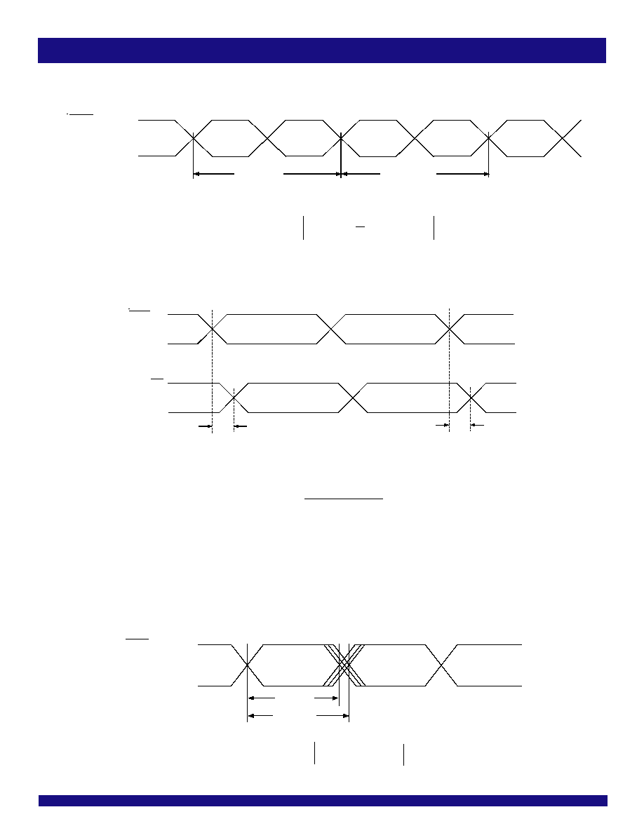
2.5V ZERO DELAY PLL CLOCK DRIVER TERACLOCK
Duty-Cycle Jitter
nQ
[1:0]
, Q
FB
Q
FB
t
W(MIN)
t
W(MAX)
t
JIT(DUTY)
= t
W(MAX)
- t
W(MIN)
JITTER AND OFFSET TIMING WAVEFORMS
t
cycle n
t
cycle n + 1
Q
FB
t
jit(cc)
t
cycle n
t
cycle n+1
=
nQ
[1:0]
, Q
FB
Cycle-to-Cycle jitter
Static Phase Offset
FB
REF
[1:0]
t
(ÿ)n
REF
[1:0]
FB
t
(ÿ)n + 1
t
(ÿ)
=
N
n = N
1
t
(ÿ)n
(N is a large number of samples)
NOTE:
1. Diagram for PE = H and TxS/RxS = L.

20
INDUSTRIAL TEMPERATURE RANGE
IDT5T2010
2.5V ZERO DELAY PLL CLOCK DRIVER TERACLOCK
Period jitter
t
jit(per) =
t
cycle n
1
fo
Q
FB
Q
FB
t
cycle n
1
fo
nQ
[1:0]
, Q
FB
nQ
[1:0]
, Q
FB
1
fo
t
jit(hper) =
t
half period n
1
2*fo
t
half period n
t
half period n+1
Q
FB
Q
FB
Q
FB
Q
FB
Half-Period jitter
NOTE:
1. 1/fo = average period.
NOTE:
1. 1/fo = average period.
21
INDUSTRIAL TEMPERATURE RANGE
IDT5T2010
2.5V ZERO DELAY PLL CLOCK DRIVER TERACLOCK
TEST CIRCUITS AND CONDITIONS
Test Circuit for Differential Input
(1)
V
DD
V
DDQ
D.U.T.
REF
[1:0]
REF
[1:0]
Pulse
Generator
3 inch, ~50
Transmission Line
3 inch, ~50
Transmission Line
V
IN
V
IN
V
DDI
R1
R2
V
DDI
R1
R2
DIFFERENTIAL INPUT TEST CONDITIONS
Symbol
V
DD
= 2.5V ± 0.2V
Unit
R1
100
R2
100
V
DDI
V
CM
*2
V
HSTL: Crossing of REF
[1:0]
and REF
[1:0]
eHSTL: Crossing of REF
[1:0]
and REF
[1:0]
V
THI
LVEPECL: Crossing of REF
[1:0]
and REF
[1:0]
V
1.8V LVTTL: V
DDI
/2
2.5V LVTTL: V
DD
/2
NOTE:
1. This input configuration is used for all input interfaces. For single-ended testing,
the REF
[1:0]
must be left floating. For testing single-ended in differential input
mode, the V
IN
should be floating.

22
INDUSTRIAL TEMPERATURE RANGE
IDT5T2010
2.5V ZERO DELAY PLL CLOCK DRIVER TERACLOCK
V
DD
V
DDQ
D.U.T.
Q
FB
Q
FB
C
L
V
DDQ
R1
R2
V
DDQ
R1
R2
C
L
REF
[1:0]
FB
FB
SW1
Test Circuit for Outputs
Test Circuit for Differential Feedback
OUTPUT TEST CONDITIONS
Symbol
V
DD
= 2.5V ± 0.2V
Unit
V
DDQ
= Interface Specified
C
L
15
pF
R1
100
R2
100
V
THO
V
DDQ
/ 2
V
SW1
TxS = MID or HIGH
Open
TxS = LOW
Closed
DIFFERENTIAL FEEDBACK TEST
CONDITIONS
Symbol
V
DD
= 2.5V ± 0.2V
Unit
V
DDQ
= Interface Specified
C
L
15
pF
R1
100
R2
100
V
OX
HSTL: Crossing of Q
FB
and Q
FB
V
eHSTL: Crossing of Q
FB
and Q
FB
V
THO
1.8V LVTTL: V
DDQ
/2
V
2.5V LVTTL: V
DDQ
/2
SW1
TxS = MID or HIGH
Open
TxS = LOW
Closed
V
DD
V
DDQ
D.U.T.
C
L
V
DDQ
R1
R2
nQ
[1:0]
REF
[1:0]
FB
FB
QFB
QFB
SW1
23
INDUSTRIAL TEMPERATURE RANGE
IDT5T2010
2.5V ZERO DELAY PLL CLOCK DRIVER TERACLOCK
ORDERING INFORMATION
IDT
XXXXX
XX
Package
Device Type
5T2010
2.5V Zero Delay PLL Clock Driver Teraclock
Plastic Ball Grid Array
Thermally Enhanced Plastic Very Fine
Pitch Quad Flat No Lead Package
BB
NL
Package
X
-40∞C to +85∞C (Industrial)
I
CORPORATE HEADQUARTERS
for SALES:
for Tech Support:
2975 Stender Way
800-345-7015 or 408-727-6116
logichelp@idt.com
Santa Clara, CA 95054
fax: 408-492-8674
(408) 654-6459
www.idt.com