1
JUNE 1999
DSC 2940/8
I/O
Control
Address
Decoder
MEMORY
ARRAY
ARBITRATION
INTERRUPT
SEMAPHORE
LOGIC
Address
Decoder
I/O
Control
R/
W
L
CE
L
OE
L
BUSY
L
A
14L
A
0L
2940 drw 01
I/O
0L
- I/O
7L
CE
L
OE
L
R/
W
L
SEM
L
INT
L
M/
S
BUSY
R
I/O
0R
-I/O
7R
A
14R
A
0R
SEM
R
INT
R
CE
R
OE
R
(2)
(1,2)
(1,2)
(2)
R/
W
R
CE
R
OE
R
R/
W
R
15
15
HIGH-SPEED
32K x 8 DUAL-PORT
STATIC RAM
Features
x
True Dual-Ported memory cells which allow simultaneous
reads of the same memory location
x
High-speed access
Military: 25/35/55ns (max.)
Industrial: 55ns (max.)
Commercial: 15/20/25/35/55ns (max.)
x
Low-power operation
IDT7007S
Active: 850mW (typ.)
Standby: 5mW (typ.)
IDT7007L
Active: 850mW (typ.)
Standby: 1mW (typ.)
x
IDT7007 easily expands data bus width to 16 bits or more
using the Master/Slave select when cascading more than
one device
x
M/S = H for BUSY output flag on Master,
M/S = L for BUSY input on Slave
x
Interrupt Flag
x
On-chip port arbitration logic
x
Full on-chip hardware support of semaphore signaling
between ports
x
Fully asynchronous operation from either port
x
TTL-compatible, single 5V (�10%) power supply
x
Available in 68-pin PGA and PLCC and a 80-pin TQFP
x
Industrial temperature range (40�C to +85�C) is available
for selected speeds
NOTES:
1. (MASTER): BUSY is output; (SLAVE): BUSY is input.
2. BUSY and INT outputs are non-tri-stated push-pull.
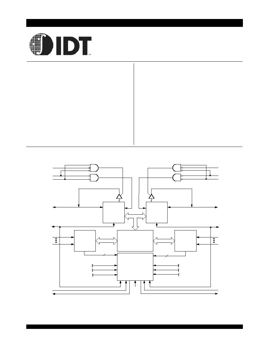
Functional Block Diagram
IDT7007S/L
IDT7007S/L
High-Speed 32K x 8 Dual-Port Static RAM Military, Industrial and Commercial Temperature Ranges
2
Description
The IDT7007 is a high-speed 32K x 8 Dual-Port Static RAM. The
IDT7007 is designed to be used as a stand-alone 256K-bit Dual-Port RAM
or as a combination MASTER/SLAVE Dual-Port RAM for 16-bit-or-more
word systems. Using the IDT MASTER/SLAVE Dual-Port RAM approach
in 16-bit or wider memory system applications results in full-speed, error-
free operation without the need for additional discrete logic.
This device provides two independent ports with separate control,
address, and I/O pins that permit independent, asynchronous access for
reads or writes to any location in memory. An automatic power down
feature controlled by CE permits the on-chip circuitry of each port to enter
a very LOW standby power mode.
Fabricated using IDTs CMOS high-performance technology, these
devices typically operate on only 850mW of power.
The IDT7007 is packaged in a 68-pin pin PGA, a 68-pin PLCC,
and an 80-pin thin quad flatpack, TQFP. Military grade product is
manufactured in compliance with the latest revision of MIL-PRF-38535
QML, Class B, making it ideally suited to military temperature applications
demanding the highest level of performance and reliability.
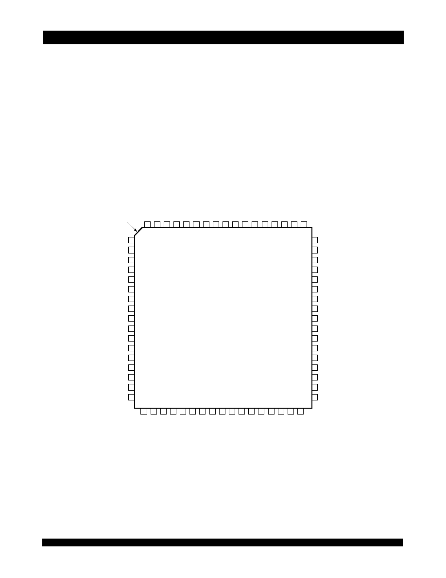
Pin Configurations
(1,2,3)
NOTES:
1. All Vcc pins must be connected to power supply.
2. All GND pins must be connected to ground supply.
3. Package body is approximately .95 in x .95 in x .17 in.
4. This package code is used to reference the package diagram.
5. This text does not indicate orientation of the actual part marking.
2940 drw 02
12
13
14
15
16
17
18
INDEX
19
20
21
22
9
8
7
6
5
4
3
2
1 68 67 66 65
27 28 29 30 31 32 33 34 35 36 37 38 39
V
C
C
V
CC
I/O
1R
I/O
2R
I/O
3R
I/O
4R
INT
L
GND
A
4L
A
3L
A
2L
A
1L
A
0L
A
3R
A
0R
A
1R
A
2R
I/O
2L
A
5L
R
/
W
L
11
10
M/
S
23
24
25
26
40 41 42 43
58
57
56
55
54
53
52
51
50
49
48
59
60
47
46
45
44
64 63 62 61
I/O
3L
GND
I/O
0R
V
CC
A
4R
BUSY
L
GND
BUSY
R
INT
R
A
1
2
R
I
/
O
7
R
N
/
C
G
N
D
O
E
R
R
/
W
R
S
E
M
R
C
E
R
O
E
L
C
E
L
N
/
C
I
/
O
0
L
I
/
O
1
L
IDT7007J
J68-1
(4)
68-Pin PLCC
Top View
(5)
I/O
4L
I/O
5L
I/O
6L
I/O
7L
I/O
5R
I/O
6R
A
1
2
L
A
1
1
R
A
1
0
R
A
9
R
A
8
R
A
7
R
A
6
R
A
5
R
A
1
1
L
A
1
0
L
A
9
L
A
8
L
A
7
L
A
6
L
A
1
3
R
A
1
3
L
A
1
4
L
A
1
4
R
S
E
M
L
3
IDT7007S/L
High-Speed 32K x 8 Dual-Port Static RAM Military, Industrial and Commercial Temperature Ranges
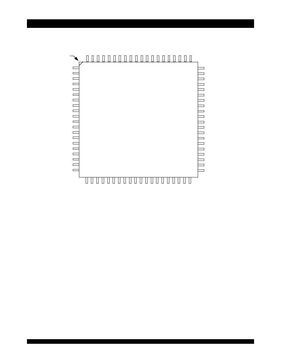
Pin Configurations
(1,2,3)
(con't.)
NOTES:
1. All Vcc pins must be connected to power supply.
2. All GND pins must be connected to ground supply.
3. Package body is approximately 14mm x 14mm x 1.4mm.
4. This package code is used to reference the package diagram.
5. This text does not indicate orientation of the actual part marking.
INDEX
I/O
2L
V
CC
GND
GND
A
4R
BUSY
L
BUSY
R
GND
M/
S
O
E
L
I
/
O
1
L
R
/
W
L
C
E
L
S
E
M
L
V
C
C
O
E
R
C
E
R
R
/
W
R
S
E
M
R
A
1
2
R
G
N
D
I/O
3L
I/O
4L
I/O
5L
I/O
6L
I/O
7L
I/O
0R
I/O
1R
I/O
2R
V
CC
I/O
3R
I/O
4R
I/O
5R
I
/
O
7
R
A
1
1
R
A
1
0
R
A
9
R
A
8
R
A
7
R
A
6
R
A
5
R
A
3R
A
2R
A
1R
A
0R
A
0L
A
1L
A
2L
A
3L
A
4L
A
6
L
A
7
L
A
8
L
A
9
L
A
1
0
L
A
1
1
L
A
1
2
L
I
/
O
0
L
2940 drw 03
A
1
3
R
A
1
3
L
7007PF
PN80-1
(4)
80-Pin TQFP
Top View
(5)
N
/
C
N
/
C
A
1
4
L
N
/
C
N
/
C
N
/
C
N
/
C
A
1
4
R
N
/
C
N
/
C
A
5L
N/C
INT
L
INT
R
N/C
N/C
N/C
I/O
6R
N/C
N/C
60
59
58
57
56
55
54
53
52
51
50
49
48
47
46
45
44
43
42
41
1
2
3
4
5
6
7
8
9
10
11
12
13
14
15
16
17
18
19
20
8
0
7
9
7
8
7
7
7
6
7
5
7
4
7
3
7
2
7
1
7
0
6
9
6
8
6
7
6
6
6
5
6
4
6
3
6
2
6
1
2
1
2
2
2
3
2
4
2
5
2
6
2
7
2
8
2
9
3
0
3
1
3
2
3
3
3
4
3
5
3
6
3
7
3
8
3
9
4
0
,
IDT7007S/L
High-Speed 32K x 8 Dual-Port Static RAM Military, Industrial and Commercial Temperature Ranges
4
NOTES:
1. All Vcc pins must be connected to power supply
2. All GND pins must be connected to power supply
3. Package body is approximately 1.8 in x 1.8 in x .16 in.
4. This package code is used to reference the package diagram.
5. This text does not indicate orientation of the actual part marking.
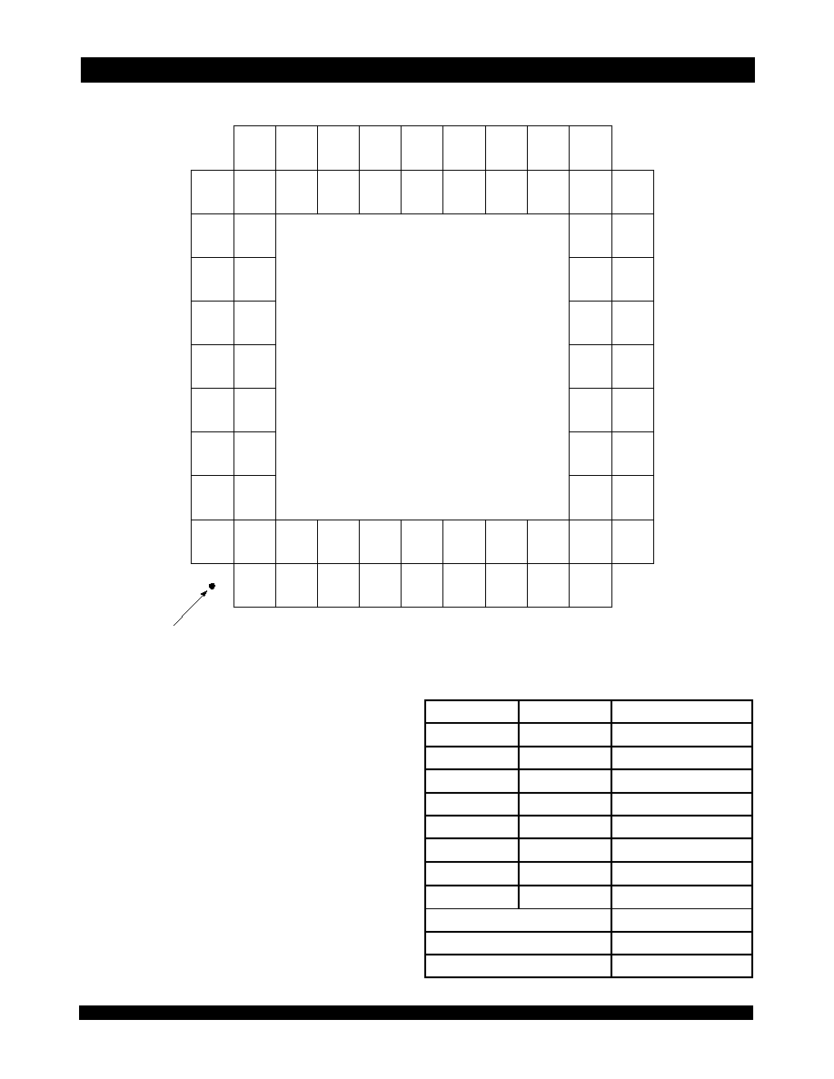
Pin Names
Pin Configurations
(1,2,3)
(con't.)
2940 drw 04
51
50
48
46
44
42
40
38
36
53
55
57
59
61
63
65
67
68
66
1
3
5
7
9
11
13
15
20
22
24
26
28
30
32
35
IDT7007G
G68-1
(4)
68-Pin PGA
Top View
(5)
A
B
C
D
E
F
G
H
J
K
L
47
45
43
41
34
21
23
25
27
29
31
33
2
4
6
8
10
12
14
16
18
19
17
56
58
60
62
64
11
10
09
08
07
06
05
04
03
02
01
52
54
49
39
37
A
5L
INT
L
SEM
L
CE
L
V
CC
OE
L
R/
W
L
I/O
0L
N/C
GND
GND
I/O
0R
V
CC
N/C
OE
R
R/
W
R
SEM
R
CE
R
GND
BUSY
R
BUSY
L
M/
S
INT
R
GND
A
1R
INDEX
A
4L
A
2L
A
0L
A
3R
A
2R
A
4R
A
5R
A
7R
A
6R
A
9R
A
8R
A
11R
A
10R
A
12R
A
0R
A
7L
A
6L
A
3L
A
1L
A
9L
A
8L
A
11L
A
10L
A
12L
V
CC
I/O
2R
I/O
3R
I/O
5R
I/O
6R
I/O
1R
I/O
4R
I/O
7R
I/O
1L
I/O
2L
I/O
4L
I/O
7L
I/O
3L
I/O
5L
I/O
6L
A
13R
A
13L
A
14R
A
14L
Left Port
Right Port
Names
CE
L
CE
R
Chip Enables
R/W
L
R/W
R
Read/Write Enable
OE
L
OE
R
Output Enable
A
0L
- A
14L
A
0R
- A
14R
Address
I/O
0L
- I/O
7L
I/O
0R
- I/O
7R
Data Input/Output
SEM
L
SEM
R
Semaphore Enable
INT
L
INT
R
Interrupt Flag
BUSY
L
BUSY
R
Busy Flag
M/S
Master or Slave Select
V
CC
Power
GND
Ground
2940 tbl 01
5
IDT7007S/L
High-Speed 32K x 8 Dual-Port Static RAM Military, Industrial and Commercial Temperature Ranges
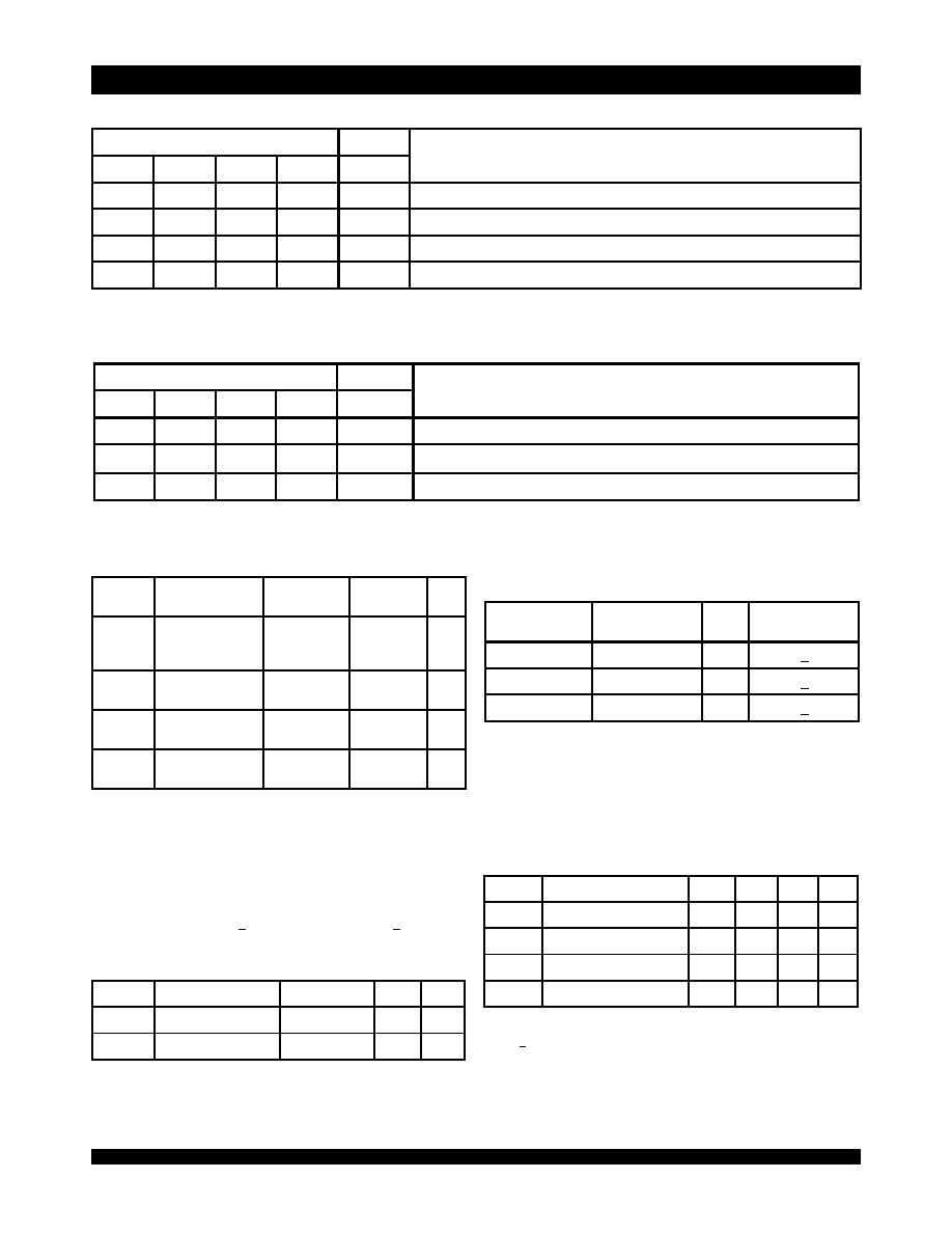
Truth Table I: Non-Contention Read/Write Control
Truth Table II: Semaphore Read/Write Control
(1)
Absolute Maximum Ratings
(1)
Recommended Operating
Conditions
Maximum Operating Temperature
and Supply Voltage
(1,2)
Capacitance
(T
A
= +25�C, f = 1.0mhz)
NOTE:
1. A
0L
A
14L
A
0R
A
14R
NOTE:
1. There are eight semaphore flags written to via I/O
0
and read from all I/O's. These eight semaphores are addressed by A
0
- A
2
.
NOTES:
1. Stresses greater than those listed under ABSOLUTE MAXIMUM RATINGS
may cause permanent damage to the device. This is a stress rating only and
functional operation of the device at these or any other conditions above those
indicated in the operational sec-tions of this specification is not implied. Exposure
to absolute maxi-mum rating conditions for extended periods may affect
reliability.
2. V
TERM
must not exceed Vcc + 10% for more than 25% of the cycle time or 10ns
maximum, and is limited to < 20mA for the period of V
TERM
> Vcc + 10%.
NOTES:
1. This is the parameter T
A
.
2. Industrial temperature: for other speeds, packages and powers contact your
sales office.
NOTES:
1. V
IL
> -1.5V for pulse width less than 10ns.
2. V
TERM
must not exceed Vcc + 10%.
NOTES:
1. This parameter is determined by device characterization but is not production
tested. TQFP package only.
2. 3dV represents the interpolated capacitance when the input and output signals
switch from 0V to 3V or from 3V to 0V.
Inputs
Outputs
Mode
CE
R/W
OE
SEM
I/O
0-7
H
X
X
H
High-Z
Deselected: Power-Down
L
L
X
H
DATA
IN
Write to Memory
L
H
L
H
DATA
OUT
Read Memory
X
X
H
X
High-Z
Outputs Disabled
2940 tbl 02
Inputs
Outputs
Mode
CE
R/W
OE
SEM
I/O
0-7
H
H
L
L
DATA
OUT
Read Semaphore Flag Data Out (I/O
0
-I/O
7
)
H
X
L
DATA
IN
Write I/O
0
into Semaphore Flag
L
X
X
L
______
Not Allowed
2940 tbl 03
Symbol
Rating
Commercial
& Industrial
Military
Unit
V
TERM
(2)
Terminal Voltage
with Respect
to GND
-0.5 to +7.0
-0.5 to +7.0
V
T
BIAS
Temperature
Under Bias
-55 to +125
-55 to +135
o
C
T
STG
Storage
Temperature
-55 to +120
-65 to +150
o
C
I
OUT
DC Output
Current
50
50
mA
2940 tbl 04
Symbol
Parameter
(1)
Conditions
(2)
Max.
Unit
C
IN
Input Capacitance
V
IN
= 3dV
9
pF
C
OUT
Output Capacitance
V
OUT
= 3dV
10
pF
2940 tbl 07
Grade
Ambient
Temperature
GND
Vcc
Military
-55
O
C to+125
O
C
0V
5.0V
+
10%
Commercial
0
O
C to +70
O
C
0V
5.0V
+
10%
Industrial
-40
O
C to +85
O
C
0V
5.0V
+
10%
2940 tbl 05
Symbol
Parameter
Min.
Typ.
Max.
Unit
V
CC
Supply Voltage
4.5
5.0
5.5
V
GND
Ground
0
0
0
V
V
IH
Input High Voltage
2.2
____
6.0
(2)
V
V
IL
Input Low Voltage
-0.5
(1)
____
0.8
V
2940 tbl 06