 | –≠–ª–µ–∫—Ç—Ä–æ–Ω–Ω—ã–π –∫–æ–º–ø–æ–Ω–µ–Ω—Ç: 707288 | –°–∫–∞—á–∞—Ç—å:  PDF PDF  ZIP ZIP |
©2000 Integrated Device Technology, Inc.
MAY 2000
DSC 3592/7
1
HIGH-SPEED
64K x 16 BANK-SWITCHABLE
DUAL-PORTED SRAM WITH
EXTERNAL BANK SELECTS
Features
x
x
x
x
x
64K x 16 Bank-Switchable Dual-Ported SRAM Architecture
≠ Four independent 16K x 16 banks
≠ 1 Megabit of memory on chip
x
x
x
x
x
Fast asynchronous address-to-data access time: 15ns
x
x
x
x
x
User-controlled input pins included for bank selects
x
x
x
x
x
Independent port controls with asynchronous address &
data busses
x
x
x
x
x
Four 16-bit mailboxes available to each port for inter-
IDT707288S/L
NOTES:
1. The first six address pins for each port serve dual functions. When
MBSEL = V
IH
, the pins serve as memory address inputs. When
MBSEL = V
IL
, the pins
serve as mailbox address inputs.
2 . Each bank has an input pin assigned that allows the user to toggle the assignment of that bank between the two ports. Refer to Truth Table I for
more details.
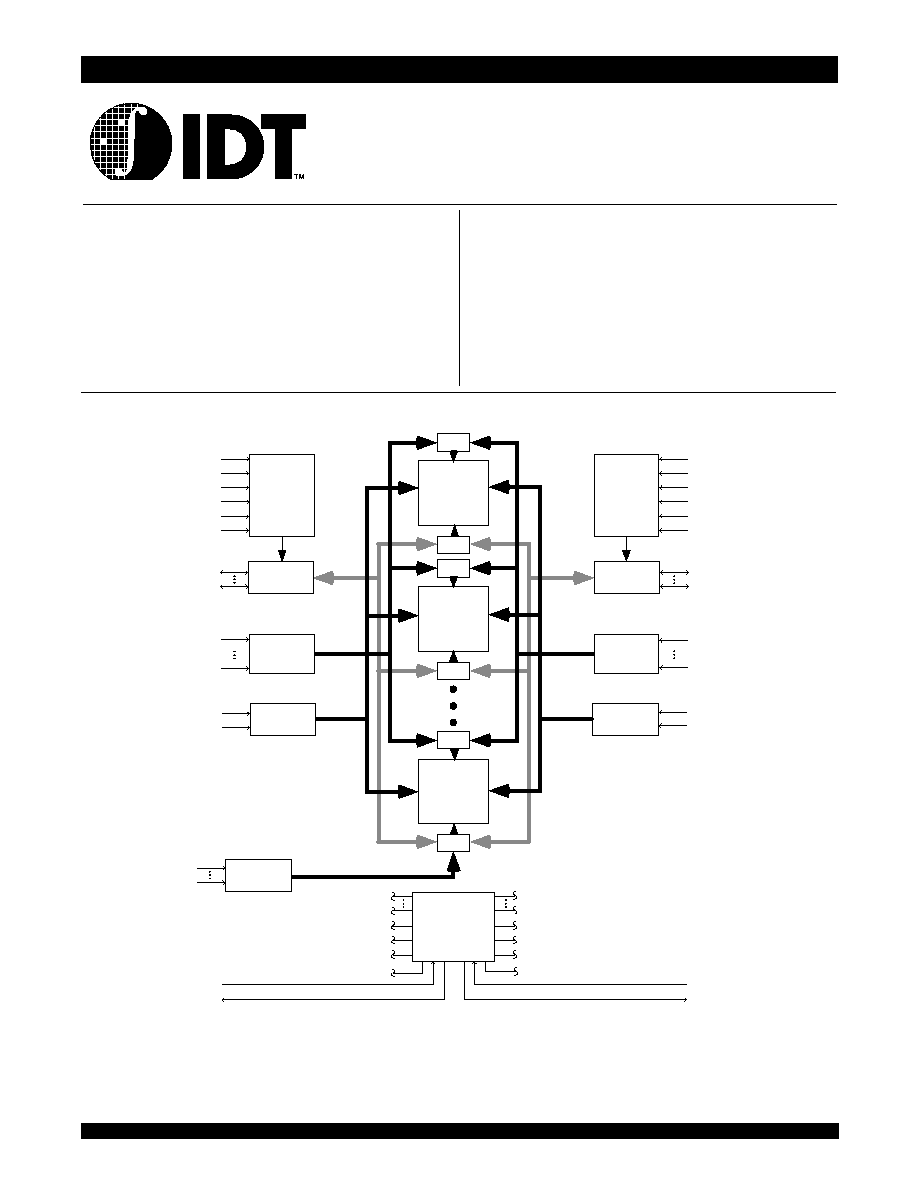
Functional Block Diagram
processor communications; interrupt option
x
x
x
x
x
Interrupt flags with programmable masking
x
x
x
x
x
Dual Chip Enables allow for depth expansion without
external logic
x
x
x
x
x
UB and LB are available for x8 or x16 bus matching
x
x
x
x
x
TTL-compatible, single 5V (±10%) power supply
x
x
x
x
x
Available in a 100-pin Thin Quad Flatpack (14mm x 14mm)
16Kx16
MEMORY
ARRAY
(BANK 3)
MUX
MUX
R/
W
L
CE
0L
CE
1L
UB
L
LB
L
OE
L
I/O
8L-15L
I/O
0L-7L
A
13L
A
0L(1)
A
5L(1)
A
0L(1)
LB
L
/
UB
L
OE
L
R/
W
L
CE
L
MAILBOX
INTERRUPT
LOGIC
16Kx16
MEMORY
ARRAY
(BANK 1)
MUX
MUX
16Kx16
MEMORY
ARRAY
(BANK 0)
MUX
MUX
CONTROL
LOGIC
I/O
CONTROL
BANK
DECODE
ADDRESS
DECODE
R/
W
R
CE
0R
CE
1R
UB
R
LB
R
OE
R
I/O
8R-15R
I/O
0R-7R
A
13R
A
0R(1)
CONTROL
LOGIC
I/O
CONTROL
BANK
DECODE
ADDRESS
DECODE
A
5R(1)
A
0R(1)
LB
R
/
UB
R
OE
R
R/
W
R
CE
R
3592 drw 01
MBSEL
R
INT
R
MBSEL
L
INT
L
BKSEL
3(2)
BKSEL
0(2)
BANK
SELECT
BA
1R
BA
0R
BA
1L
BA
0L

6.42
IDT707288S/L
High-Speed 64K x 16 Dual-Port Static RAM Industrial and Commercial Temperature Ranges
2
Description
The IDT707288 is a high-speed 64K x 16 (1M bit) Bank-Switchable
Dual-Ported SRAM organized into four independent 16K x 16 banks. The
device has two independent ports with separate control, address, and
I/O pins for each port, allowing each port to asynchronously access
any 16K x 16 memory block not already accessed by the other port.
Accesses by the ports into specific banks are controlled via bank select pin
inputs under the user's control. Mailboxes are provided to allow inter-
processor communication. Interrupts are provided to indicate mailbox
writes have occurred. An automatic power down feature controlled by
the chip enables (
CE
0
and CE
1
) permits the on-chip circuitry of each port
to enter a very low standby power mode and allows fast depth expansion.
The IDT707288 offers a maximum address-to-data access time as fast
as 15ns, and is packaged in a 100-pin Thin Quad Flatpack (TQFP).
Functionality
The IDT707288 is a high-speed asynchronous 64K x 16 Bank-
Switchable Dual-Ported SRAM, organized in four 16K x 16 banks. The
two ports are permitted independent, simultaneous access into separate
banks within the shared array. There are four user-controlled Bank Select
input pins, and each of these pins is associated with a specific bank within
the memory array. Access to a specific bank is gained by placing the
associated Bank Select pin in the appropriate state: V
IH
assigns the bank
to the left port, and V
IL
assigns the bank to the right port (See Truth Table
IV). Once a bank is assigned to a particular port, the port has full access
to read and write within that bank. Each port can be assigned as many
banks within the array as needed, up to and including all four banks.
The IDT707288 provides mailboxes to allow inter-processor commu-
nication. Each port has four 16-bit mailbox registers available to which it
can write and read and which the opposite port can read only. These
mailboxes are external to the common SRAM array, and are accessed
by setting
MBSEL = V
IL
while setting
CE = V
IH
. Each mailbox has an
associated interrupt: a port can generate an interrupt to the opposite port
by writing to the upper byte of any one of its four 16-bit mailboxes. The
interrupted port can clear the interrupt by reading the upper byte. This read
will not alter the contents of the mailbox.
If desired, any source of interrupt can be independently masked via
software. Two registers are provided to permit interpretation of interrupts:
the Interrupt Cause Register and the Interrupt Status Register. The
Interrupt Cause Register gives the user a snapshot of what has caused
the interrupt to be generated - the specific mailbox written to. The
information in this register provides post-mask signals: interrupt sources
that have been masked will not be updated. The Interrupt Status Register
gives the user the status of all bits that could potentially cause an interrupt
regardless of whether they have been masked. Truth Table V gives a
detailed explanation of the use of these registers.
6.42
IDT707288S/L
High-Speed 64K x 16 Dual-Port Static RAM Industrial and Commercial Temperature Ranges
3
INDEX
1
2
3
4
5
6
7
8
9
10
11
12
13
14
15
16
17
18
19
20
21
22
23
24
25
75
74
73
72
71
70
69
68
67
66
65
64
63
62
61
60
59
58
57
56
55
54
53
52
51
26 27 28 29 30 31 32 33 34 35 36 37 38 39 40 41 42 43 44 45 46 47 48 49 50
100 99 98 97 96 95 94 93 92 91 90 89 88 87 86 85 84 83 82 81 80 79 78 77 76
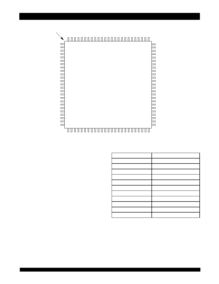
IDT707288PF
PN100-1
(4)
100-Pin TQFP
Top View
(5)
GND
OE
R
R/
W
R
MBSEL
R
CE
1R
CE
0R
BKSEL
3
NC
GND
A
9R
A
10R
A
8R
A
7R
A
6R
A
11R
I/O
10R
I/O
11R
I/O
12R
I/O
13R
I/O
14R
I/O
15R
GND
UB
R
LB
R
3592 drw 02
I/O
15L
GND
OE
L
R/
W
L
MBSEL
L
CE
1L
CE
0L
Vcc
BKSEL
0
A
11L
A
10L
NC
A
9L
A
8L
A
7L
A
6L
I/O
10L
I/O
11L
I/O
12L
I/O
13L
I/O
14L
UB
L
LB
L
GND
I
/
O
5
R
I
/
O
4
R
I
/
O
3
R
I
/
O
2
R
I
/
O
0
R
I
/
O
0
L
G
N
D
I
/
O
2
L
I
/
O
4
L
I
/
O
5
L
I
/
O
6
L
I
/
O
7
L
I
/
O
3
L
I
/
O
1
R
I
/
O
7
R
I
/
O
8
R
I
/
O
9
R
I
/
O
8
L
I
/
O
9
L
I
/
O
6
R
A
4
R
A
5
L
A
4
L
A
3
R
A
0
R
A
1
2
R
I
N
T
R
I
N
T
L
B
K
S
E
L
1
A
3
L
A
5
R
G
N
D
V
c
c
I
/
O
1
L
V
c
c
G
N
D
A
13R
N
C
B
A
0
R
B
A
1
R
A
1
R
A
2
R
B
K
S
E
L
2
G
N
D
N
C
A
0
L
A
1
2
L
B
A
0
L
B
A
1
L
A
1
L
A
2
L
A
13L
,
Pin Names
NOTES:
1. All V
CC
pins must be connected to power supply.
2. All GND pins must be connected to ground supply.
3. Package body is approximately 14mm x 14mm x 1.4mm.
4. This package code is used to reference the package diagram.
5. This text does not indicate orientation of the actual part-marking.
NOTES:
1. Duplicated per port.
2. Each bank has an input pin assigned that allows the user to toggle the assignment
of that bank between the two ports. Refer to Truth Table IV for more details. When
changing the bank assignments, accesses of the affected banks must be
suspended. Accesses may continue uninterrupted in banks that are not being
reallocted.
3. Generated upon mailbox access.
4. All Vcc pins must be connected to power supply.
5. All GND pins must be connected to ground supply.
6. The first six address pins (A
0
-A
5
) for each port serve dual functions. When
MBSEL
= V
IH
, the pins serve as memory address inputs. When
MBSEL = V
IL
, the pins
serve as mailbox address inputs (A
6
-A
13
are ignored).
Pin Configurations
(1,2,3)
A
0
- A
13
(1,6)
Address Inputs
BA
0
- BA
1
(1)
Bank Address Inputs
MBSEL
(1)
Mailbox Access Control Gate
BKSEL
0-3
(2)
Bank Select Inputs
R/
W
(1)
Read/Write Enable
OE
(1)
Output Enable
CE
0
,
CE
1
(1)
Chip Enables
UB, LB
(1)
I/O Byte Enables
I/O
0
- I/O
15
(1)
Bidirectional Data Input/Output
INT
(1)
Interrupt Flag (Output)
(3)
V
CC
(4)
+5VPower
GND
(5)
Ground
3592 tbl 01
6.42
IDT707288S/L
High-Speed 64K x 16 Dual-Port Static RAM Industrial and Commercial Temperature Ranges
4
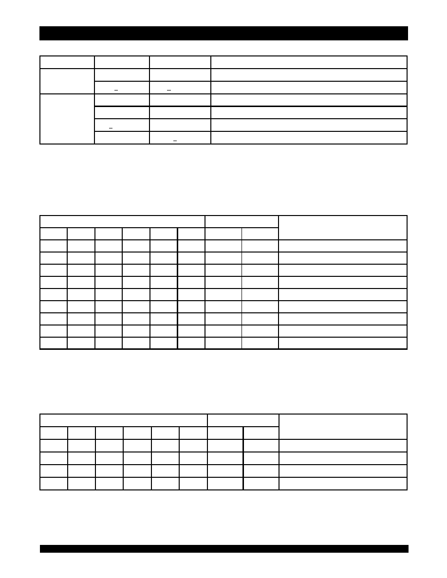
Truth Table III Mailbox Read/Write Contro
l
(1)
NOTES:
1. Chip Enable references are shown above with the actual
CE
0
and CE
1
levels;
CE is a reference only.
2. Port "A" and "B" references are located where
CE is used.
3. "H" = V
IH
and "L" = V
IL
.
4.
CE and MBSEL cannot both be active at the same time.
Truth Table I Chip Enable
(1,2,3,4)
Truth Table II Non-Contention Read/Write Control
NOTES:
1. BA
0L
- BA
1L
BA
0R
- BA
1R
: cannot access same bank simultaneously from both ports.
2. Refer to Truth Table I.
3.
CE and MBSEL cannot both be active at the same time.
NOTES:
1. There are four mailbox locations per port written to and read from all the I/O's (I/O
0
-I/O
15
). These four mailboxes are addressed by A
0
-A
5.
Refer to Truth Table V.
2. Refer to Truth Table I.
3. Each mailbox location contains a 16-bit word, controllable in bytes by setting input levels to
UB and LB appropriately.
CE
CE
0
CE
1
Mode
L
V
IL
V
IH
Port Selected (TTL Active)
< 0.2V
>V
CC
-0.2V
Port Selected (CMOS Active)
H
V
IH
X
Port Deselected (TTL Inactive)
X
V
IL
Port Deselected (TTL Inactive)
>V
CC
-0.2V
X
Port Deselected (CMOS Inactive)
X
<0.2V
Port Deselected (CMOS Inactive)
3592 tbl 02
Inputs
(1)
Outputs
Mode
CE
(2)
R/
W
OE
UB
LB
MBSEL
I/O
8-15
I/O
0-7
H
X
X
X
X
H
High-Z
High-Z
Deselcted: Power-Down
X
(3)
X
X
H
H
X
(3)
High-Z
High-Z
Both Bytes Deselected
L
L
X
L
H
H
DATA
IN
High-Z
Write to Upper Byte Only
L
L
X
H
L
H
High-Z
DATA
IN
Write to Lower Byte Only
L
L
X
L
L
H
DATA
IN
DATA
IN
Write to Both Bytes
L
H
L
L
H
H
DATA
OUT
High-Z
Read Upper Byte Only
L
H
L
H
L
H
High-Z
DATA
OUT
Read Lower Byte Only
L
H
L
L
L
H
DATA
OUT
DATA
OUT
Read Both Bytes
X
(3)
X
H
X
X
X
(3)
High-Z
High-Z
Outputs Disabled
3592 tbl 03
Inputs
Outputs
Mode
CE
(2)
R/
W
OE
UB
LB
MBSEL
I/O
8-15
I/O
0-7
H
H
L
X
(3)
X
(3)
L
DATA
OUT
DATA
OUT
Read Data from Mailbox,
clears interrupt
H
H
L
L
L
L
DATA
OUT
DATA
OUT
Read Data from Mailbox,
clears interrupt
H
L
X
L
(3)
L
(3)
L
DATA
IN
DATA
IN
Write Data into Mailbox
L
X
X
X
X
L
____
____
Not Allowed
3592 tbl 04

6.42
IDT707288S/L
High-Speed 64K x 16 Dual-Port Static RAM Industrial and Commercial Temperature Ranges
5
Absolute Maximum Ratings
(1)
DC Electrical Characteristics Over the Operating
Temperature and Supply Voltage Range
(V
CC
= 5.0V ± 10%)
Capacitance
(1)
(T
A
= +25∞C, f = 1.0mhz) TQFP Package
Recommended DC Operating
Conditions
Maximum Operating Temperature
and Supply Voltage
(1)
NOTES:
1. Stresses greater than those listed under ABSOLUTE MAXIMUM RATINGS may
cause permanent damage to the device. This is a stress rating only and
functional operation of the device at these or any other conditions above those
indicated in the operational sections of this specification is not implied. Exposure
to absolute maximum rating conditions for extended periods may affect
reliability.
2. V
TERM
must not exceed Vcc + 10% for more than 25% of the cycle time or 10ns
maximum, and is limited to < 20mA for the period of V
TERM
> Vcc + 10%.
NOTES:
1. V
IL
> -1.5V for pulse width less than 10ns.
2. V
TERM
must not exceed Vcc + 10%.
NOTES:
1. This parameter is determined by device characterization but is not production
tested.
2. 3dV represents the interpolated capacitance when the input and output signals
switch from 0V to 3V or from 3V to 0V.
3. C
OUT
represents C
I/O
as well.
NOTE:
1. At Vcc
<
2.0V, input leakages are undefined.
NOTES:
1. This is the parameter T
A
. This is the "instant on" case temperature.
Symbol
Rating
Commercial
& Industrial
Unit
V
TERM
(2)
Terminal Voltage
with Respect
to GND
-0.5 to +7.0
V
T
BIAS
Temperature
Under Bias
-55 to +125
o
C
T
STG
Storage
Temperature
-65 to +150
o
C
I
OUT
DC Output
Current
50
mA
3592 tbl 05
Grade
Ambient
Temperature
GND
Vcc
Commercial
0
O
C to +70
O
C
0V
5.0V
+
10%
Industrial
-40
O
C to +85
O
C
0V
5.0V
+
10%
3592 tbl 06
Symbol
Parameter
Min.
Typ.
Max.
Unit
V
CC
Supply Voltage
4.5
5.0
5.5
V
GND
Ground
0
0
0
V
V
IH
Input High Voltage
2.2
____
6.0
(2)
V
V
IL
Input Low Voltage
-0.5
(1)
____
0.8
V
3592 tbl 07
Symbol
Parameter
Conditions
(2)
Max.
Unit
C
IN
Input Capacitance
V
IN
= 3dV
9
pF
C
OUT
(3)
Output Capacitance
V
OUT
= 3dV
10
pF
3592 tbl 08
Symbol
Parameter
Test Conditions
707288S
707288L
Unit
Min.
Max.
Min.
Max.
|I
LI
|
Input Leakage Current
(1)
V
CC
= 5.5V, V
IN
= 0V to V
CC
___
10
___
5
µ A
|I
LO
|
Output Leakage Current
CE = V
IH
,
MBSEL = V
IH
, V
OUT
= 0V to V
CC
___
10
___
5
µ A
V
OL
Output Low Voltage
I
OL
= +4mA
___
0.4
___
0.4
V
V
OH
Output High Voltage
I
OH
= -4mA
2.4
___
2.4
___
V
3592 tbl 09