 | –≠–ª–µ–∫—Ç—Ä–æ–Ω–Ω—ã–π –∫–æ–º–ø–æ–Ω–µ–Ω—Ç: 709149 | –°–∫–∞—á–∞—Ç—å:  PDF PDF  ZIP ZIP |
©1999 Integrated Device Technology, Inc.
SEPTEMBER 1999
DSC-3494/4
1
Features
x
x
x
x
x
Architecture based on Dual-Port SRAM cells
Allows full simultaneous access from both ports
x
x
x
x
x
High-speed clock-to-data output times
Commercial: 8/10/12ns (max.)
x
x
x
x
x
Low-power operation
IDT709149S
Active: 1500mW (typ.)
Standby: 75mW (typ.)
x
x
x
x
x
4K X 9 bits
x
x
x
x
x
Synchronous operation
4ns setup to clock, 1ns hold on all control, data, and
address inputs
Data input, address, and control registers
Fast 8ns clock to data out
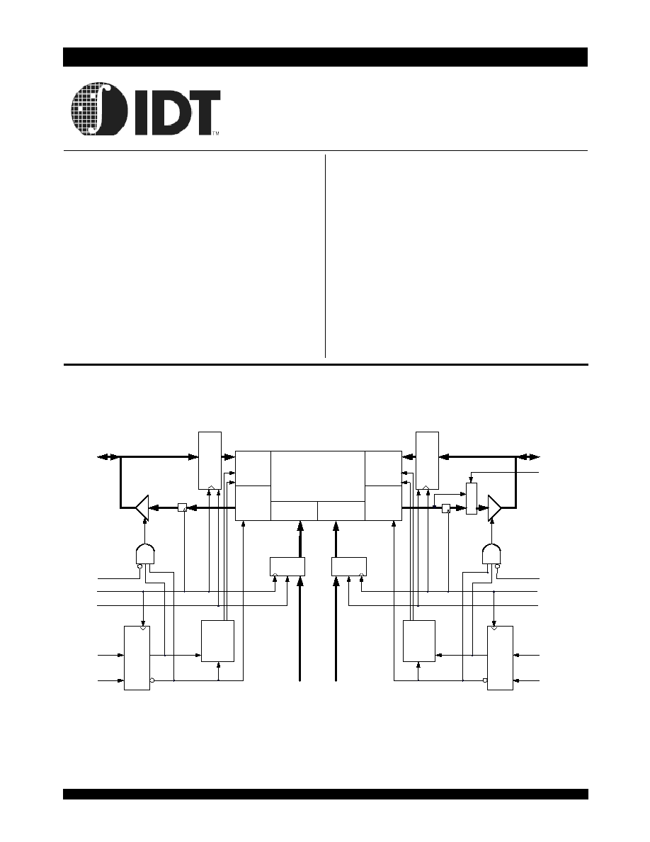
HIGH-SPEED 36K (4K x 9-BIT)
SYNCHRONOUS PIPELINED
DUAL-PORT SRAM
IDT709149S
Functional Block Diagram
WRITE
LOGIC
SENSE
AMPS
DECODER
CLK
R
R/
W
R
REG
CE
R
OE
R
CLKEN
R
MEMOR
Y
ARRAY
en
WRITE
LOGIC
SENSE
AMPS
DECODER
A
0L
-A
11L
CLK
L
R/
W
L
REG
CE
L
OE
L
REG
CLKEN
L
MEMORY
ARRAY
en
3494 drw 01
I/O
0-8R
A
0R
-A
11R
REG
Self-
timed
Write
Logic
I/O
0-8L
Self-
timed
Write
Logic
R
E
GI
ST
ER
R
E
GI
ST
ER
0/1
1
0
FT/PIPED
R
x
x
x
x
x
13ns cycle time, 76MHz operation in pipeline mode
Self-timed write allows for fast cycle times
x
x
x
x
x
TTL-compatible, singles 5V (±10%) power supply
x
x
x
x
x
Clock Enable feature
x
x
x
x
x
Guaranteed data output hold times
x
x
x
x
x
Industrial temperature range (40∞C to +85∞C) is available
for selected speeds.
Description
The IDT709149 is a high-speed 4K x 9 bit synchronous Dual-Port
SRAM. The memory array is based on Dual-Port memory cells to allow
simultaneous access from both ports. Registers on control, data, and
address inputs provide low set-up and hold times. The timing latitude
provided by this approach will allow systems to be designed with very

6.42
IDT709149S
High-Speed 36K (4K x 9-bit) Synchronous Pipelined Dual-Port Static RAM Industrial and Commercial Temperature Ranges
2
NOTES:
1. All V
CC
pins must be connected to power supply.
2. All ground pins must be connected to ground supply.
3. Package body is approximately 14mm x 14mm x 1.4mm.
4, This package code is used to reference the package diagram.
5. This text does not indicate the orientaion of the actual part-marking.
Reference
N/C
1
2
3
4
5
6
7
8
9
10
11
12
13
14
15
16
17
18
19
20
21 22 23 24 25 26 27 28 29 30 31 32 33 34 35 36 37 38 39 40
80 79 78 77 76 75 74 73 72 71 70 69 68 67 66 65 64 63 62 61
60
59
58
57
56
55
54
53
52
51
50
49
48
47
46
45
44
43
42
41
3494 drw 02
IDT709149PF
PN80-1
(4)
80-Pin TQFP
Top View
(5)
N/C
A
6L
A
7L
A
8L
A
9L
A
10L
A
11L
N/C
OE
L
V
CC
R/
W
L
N/C
CE
L
GND
I/O
8L
I/O
7L
I/O
6L
N/C
A
7R
A
8R
A
9R
A
10R
A
11R
N/C
OE
R
GND
GND
R/
W
R
N/C
CE
R
GND
I/O
8R
I/O
7R
I/O
6R
N/C
C
L
K
E
N
L
C
L
K
E
N
R
N/C
N/C
FT
/PIPED
R
V
CC
N
/
C
N
/
C
I
/
O
5
L
V
C
C
I
/
O
4
L
I
/
O
3
L
I
/
O
2
L
I
/
O
1
L
I
/
O
0
L
G
N
D
G
N
D
I
/
O
0
R
I
/
O
1
R
I
/
O
2
R
I
/
O
3
R
V
C
C
I
/
O
4
R
I
/
O
5
R
N
/
C
N
/
C
N
/
C
N
/
C
A
5
L
A
4
L
A
3
L
A
2
L
A
1
L
A
0
L
C
L
K
L
C
L
K
R
A
0
R
A
1
R
A
2
R
A
3
R
A
4
R
A
5
R
A
6
R
N
/
C
,
Pin Configurations
(1,2,3)
short cycle times. This device has been optimized for applications
having unidirectional data flow or bi-directional data flow in bursts, by
utilizing input data registers.
The IDT709149 utilizes a 9-bit wide data path to allow for parity at
the user's option. This feature is especially useful in data communica-
tion applications where it is necessary to use a parity bit for transmis-
sion/reception error checking.
Fabricated using IDTs CMOS high-performance technology, these
Dual-Ports typically operate on only 800mW of power at maximum
high-speed clock-to-data output times as fast as 8ns. An automatic
power down feature, controlled by CE, permits the on-chip circuitry
of each port to enter a very low standby power mode.
The IDT709149 is packaged in an 80-pin TQFP.

6.42
IDT709149S
High-Speed 36K (4K x 9-bit) Synchronous Pipelined Dual-Port Static RAM Industrial and Commercial Temperature Ranges
3
Recommended DC Operating
Conditions
NOTES:
1. Stresses greater than those listed under ABSOLUTE MAXIMUM RATINGS may
cause permanent damage to the device. This is a stress rating only and functional
operation of the device at these or any other conditions above those indicated in the
operational sections of this specification is not implied. Exposure to absolute
maximum rating conditions for extended periods may affect reliability.
2. V
TERM
must not exceed V
cc
+ 10% for more than 25% of the cycle time or 10ns
maximum, and is limited to < 20mA for the period of V
TERM
> V
cc
+ 10%.
Absolute Maximum Ratings
(1)
Maximum OperatingTemperature
and Supply Voltage
(1,2)
NOTES:
1. These parameters are determined by device characterization, but are not produc-
tion tested.
2. 3dV references the interpolated capacitance when the input and output switch from
0V to 3V or from 3V to 0V.
Capacitance
(T
A
= +25∞C, f = 1.0MH
z
)
N
OTES:
1. This is the parameter T
A
.
2. Industrial temperature: for specific speeds, packages and powers contact your
sales office.
NOTES:
1. V
IL
> -1.5V for pulse width less than 10ns.
2. V
TERM
must not exceed V
cc
+ 10%.
DC Electrical Characteristics Over the Operating
Temperature and Supply Voltage Range
(V
CC
= 5.0V ± 10%)
NOTE:
1. At V
CC
< 2.0V, input leakages are undefined
Symbol
Rating
Commercial
& Industrial
Unit
V
TERM
(2)
Terminal Voltage
with Respect
to GND
-0.5 to +7.0
V
V
TERM
(2)
Terminal Voltage
-0.5 to V
CC
V
T
BIAS
Temperature
Under Bias
-55 to +125
o
C
T
STG
Storage
Temperature
-55 to +125
o
C
I
OUT
DC Output Current
50
mA
3494 tbl 01
Grade
Ambient Temperature
GND
Vcc
Commercial
0
O
C to +70
O
C
0V
5.0V
+
10%
Industrial
-40
O
C to +85
O
C
0V
5.0V
+
10%
3494 tbl 02
Symbol
Parameter
Min.
Typ.
Max.
Unit
V
CC
Supply Voltage
4.5
5.0
5.5
V
GND
Ground
0
0
0
V
V
IH
Input High Voltage
2.2
____
6.0
(2)
V
V
IL
Input Low Voltage
-0.5
(1)
____
0.8
V
3494 tbl 03
Symbol
Parameter
Conditions
Max. Unit
C
IN
Input Capacitance
V
IN
= 3dV
8
pF
C
OUT
Output Capacitance
V
OUT
= 3dV
9
pF
3494 tbl 04
Symbol
Parameter
Test Conditions
709149S
Unit
Min.
Max.
|I
LI
|
Input Leakage Current
(1)
V
CC
= 5.5V, V
IN
= 0V to V
CC
___
10
µA
|I
LO
|
Output Leakage Current
V
OUT
= 0V to V
CC
___
10
µA
V
OL
Output Low Voltage
I
OL
= +4mA
___
0.4
V
V
OH
Output High Voltage
I
OH
= -4mA
2.4
___
V
3494 tbl 05

6.42
IDT709149S
High-Speed 36K (4K x 9-bit) Synchronous Pipelined Dual-Port Static RAM Industrial and Commercial Temperature Ranges
4
1
2
3
4
5
6
7
8
20 40
100
60 80
120 140 160 180 200
tCD
(Typical, ns)
Capacitance (pF)
3494 drw 05
-1
0
9pF is the I/O capacitance
of this device, and 30pF is the
AC Test Load Capacitance
,
Figure 3. Typical Output Derating (Lumped Capacitive Load).
Figure 1. AC Output Test load.
Figure 2. Output Test Load
(For t
CKLZ
, t
CKHZ
, t
OLZ
, and t
OHZ
).
*Including scope and jig.
DC Electrical Characteristics Over the Operating
Temperature and Supply Voltage Range
(4,5)
(V
CC
= 5V ± 10%)
AC Test Conditions
NOTES:
1. At f = f
MAX
, address and control lines (except Output Enable) are cycling at the maximum frequency clock cycle of 1/t
CLK
, using "AC TEST CONDITIONS" at input levels of
GND to 3V.
2. f = 0 means no address, clock, or control lines change. Applies only to input at CMOS level standby.
3. Port "A" may be either left or right port. Port "B" is the opposite from port "A".
4. Vcc = 5V, T
A
= 25∞C for Typ, and are not production tested. I
CC DC
= 150mA (Typ).
5. Industrial temperature: for specific speeds, packages and powers contact your sales office.
709149S8
Com'l Only
709149S10
Com'l Only
709149S12
Com'l Only
Symbol
Parameter
Test Condition
Version
Typ.
Max.
Typ.
Max.
Typ.
Max.
Unit
I
CC
Dynamic Operating
Current
(Both Ports Active)
CE
L
and CE
R
= V
IL
,
Outputs Open
f = f
MAX
(1)
COM'L
____
320
____
310
____
300
mA
IND
____
____
____
____
____
____
I
SB1
Standby Current
(Both Ports - TTL
Level Inputs)
CE
L
and CE
R
= V
IH
f = f
MAX
(1)
COM'L
____
150
____
150
____
140
mA
IND
____
____
____
____
____
____
I
SB2
Standby Current
(One Port - TTL
Level Inputs)
CE
"A"
= V
IL
and CE
"B"
= V
IH
(3)
Active Port Outputs Open,
f=f
MAX
(1)
COM'L
____
230
____
220
____
210
mA
IND
____
____
____
____
____
____
I
SB3
Full Standby Current
(Both Ports - All
CMOS Level Inputs)
CE
L
and
CE
R
> V
CC
- 0.2V,
V
IN
> V
CC
- 0.2V or
V
IN
< 0.2V, f = 0
(2)
COM'L
____
15
____
15
____
15
mA
IND
____
____
____
____
____
____
I
SB4
Full Standby Current
(One Port - All
CMOS Level Inputs)
CE
"A"
< 0.2V and
CE
"B"
> V
CC
- 0.2V
(3)
V
IN
> V
CC
- 0.2V or V
IN
< 0.2V
Active Port Outputs Open,
f = f
MAX
(1)
COM'L
____
220
____
210
____
200
mA
IND
____
____
____
____
____
____
3494 tbl 06
Input Pulse Levels
Input Rise/Fall Times
Input Timing Reference Levels
Output Reference Levels
Output Load
GND to 3.0V
3ns Max.
1.5V
1.5V
Figures 1,2 and 3
3494 tbl 07
3494 drw 04
893
30pF
347
5V
DATA
OUT
893
5pF*
347
5V
DATA
OUT
3494 drw 03
,
6.42
IDT709149S
High-Speed 36K (4K x 9-bit) Synchronous Pipelined Dual-Port Static RAM Industrial and Commercial Temperature Ranges
5
AC Electrical Characteristics Over the Operating Temperature Range
(Read and Write Cycle Timing)
(4)
(Commercial: V
CC
= 5V ± 10%, T
A
= 0∞C to +70∞C)
NOTES:
1. Transition is measured ±200mV from Low or High-impedance voltage with the Output Test Load (Figure 2).
2. This parameter is guaranteed by device characterization, but is not production tested.
3. The Pipelined output parameters (t
CYC2
, t
CD2
) always apply to the Left Port. The Right Port uses the Pipelined t
CYC2
and t
CD2
when FT/PIPED
R
= V
IH
and the Flow-
Through parameters (t
CYC1
, t
CD1
) when FT/PIPED
R
= V
IL.
4. Industrial temperature: for specific speeds, packages and powers contact your sales office.
709149S8
Com'l Only
709149S10
Com'l Only
709124S12
Com'l Only
Unit
Symbol
Parameter
Min.
Max.
Min.
Max.
Min.
Max.
t
CYC1
Clock Cycle Time (Flow-Through)
(3)
16
____
20
____
20
____
ns
t
CYC2
Clock Cycle Time (Pipelined)
(3)
13
____
15
____
16
____
ns
t
CH1
Clock High Time (Flow-Through)
(3)
6
____
7
____
8
____
ns
t
CL1
Clock Low Time (Flow-Through)
(3)
6
____
7
____
8
____
ns
t
CH2
Clock High Time (Pipelined)
(3)
6
____
6
____
6
____
ns
t
CL2
Clock Low Time (Pipelined)
(3)
6
____
6
____
6
____
ns
t
CD1
Clock to Data Valid (Flow-Through)
(3)
____
12
____
15
____
20
ns
t
CD2
Clock to Data Valid (Pipelined)
(3)
____
8
____
10
____
12
ns
t
S
Registered Signal Set-up Time
4
____
4
____
5
____
ns
t
H
Registered Signal Hold Time
1
____
1
____
1
____
ns
t
DC
Data Output Hold After Clock High
1
____
1
____
1
____
ns
t
CKLZ
Clock High to Output Low-Z
(1,2)
2
____
2
____
2
____
ns
t
CKHZ
Clock High to Output High-Z
(1,2)
____
7
____
7
____
9
ns
t
OE
Output Enable to Output Valid
____
8
____
8
____
10
ns
t
OLZ
Output Enable to Output Low-Z
(1,2)
0
____
0
____
0
____
ns
t
OHZ
Output Disable to Output High-Z
(1,2)
____
7
____
7
____
9
ns
t
SCK
Clock Enable, Disable Set-Up Time
4
____
4
____
5
____
ns
t
HCK
Clock Enable, Disable Hold Time
1
____
1
____
1
____
ns
t
CWDD
Write Port Clock High to Read Data Delay
____
25
____
30
____
35
ns
3494 tbl 08