 | –≠–ª–µ–∫—Ç—Ä–æ–Ω–Ω—ã–π –∫–æ–º–ø–æ–Ω–µ–Ω—Ç: 709269 | –°–∫–∞—á–∞—Ç—å:  PDF PDF  ZIP ZIP |
©2000 Integrated Device Technology, Inc.
APRIL 2000
DSC-3493/8
1
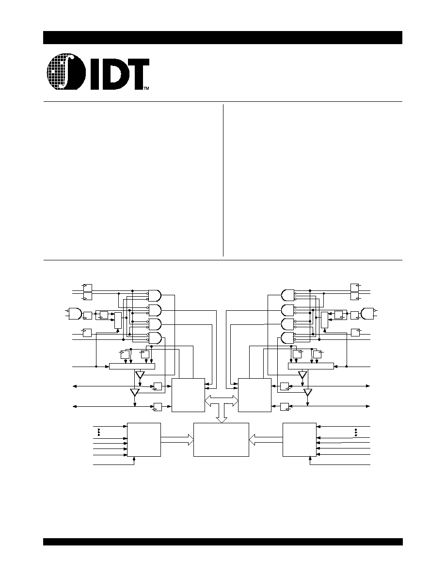
Functional Block Diagram
Features:
x
True Dual-Ported memory cells which allow simultaneous
access of the same memory location
x
High-speed clock to data access
≠ Commercial: 9/12/15ns (max.)
x
Low-power operation
≠ IDT709269S
Active: 950mW (typ.)
Standby: 5mW (typ.)
≠ IDT709269L
Active: 950mW (typ.)
Standby: 1mW (typ.)
x
Flow-through or Pipelined output mode on either port via
the
FT/PIPE pin
x
Counter enable and reset features
x
Dual chip enables allow for depth expansion without
additional logic
HIGH-SPEED 16K x 16
SYNCHRONOUS PIPELINED
DUAL-PORT STATIC RAM
PRELIMINARY
IDT709269S/L
x
Full synchronous operation on both ports
≠ 4ns setup to clock and 1ns hold on all control, data, and
address inputs
≠ Data input, address, and control registers
≠ Fast 9ns clock to data out in the Pipelined output mode
≠ Self-timed write allows fast cycle time
≠ 15ns cycle time, 66MHz operation in Pipelined output mode
x
Separate upper-byte and lower-byte controls for
multiplexed bus and bus matching compatibility
x
TTL- compatible, single 5V (±10%) power supply
x
Industrial temperature range (≠40∞C to +85∞C) is
available for selected speeds
x
Available in a 100-pin Thin Quad Flatpack (TQFP) package
0a 1a
0b 1b
0/1
a
b
1
0/1
0
FT
/PIPE
R
R/
W
R
UB
R
LB
R
CE
0R
OE
R
CE
1R
I/O
Control
MEMORY
ARRAY
Counter/
Address
Reg.
I/O
Control
3493 drw 01
A
13R
A
0R
CLK
R
ADS
R
CNTEN
R
CNTRST
R
I/O
8L
-I/O
15L
I/O
0L
-I/O
7L
I/O
8R
-I/O
15R
I/O
0R
-I/O
7R
A
0L
CLK
L
ADS
L
A
13L
CNTEN
L
CNTRST
L
Counter/
Address
Reg.
R/
W
L
UB
L
LB
L
CE
0L
OE
L
CE
1L
FT
/PIPE
L
1
0/1
0
1a 0a
1b 0b
0/1
b
a
6.42
IDT709269S/L Preliminary
High-Speed 16K x 16 Synchronous Pipelined Dual-Port Static RAM Industrial and Commercial Temperature Ranges
2
Index
1
2
3
4
5
6
7
8
9
10
11
12
13
14
15
16
17
18
19
20
21
22
23
24
25
75
74
73
72
71
70
69
68
67
66
65
64
63
62
61
60
59
58
57
56
55
54
53
52
51
26 27 28 29 30 31 32 33 34 35 36 37 38 39 40 41 42 43 44 45 46 47 48 49 50
100 99 98 97 96 95 94 93 92 91 90 89 88 87 86 85 84 83 82 81 80 79 78 77 76
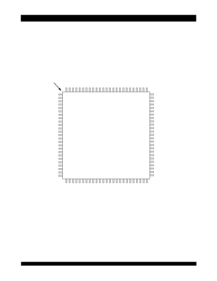
IDT709269PF
PN100-1
(4)
100-PIN TQFP
TOP VIEW
(5)
NC
I/O
10R
I/O
11R
I/O
12R
I/O
13R
I/O
14R
I/O
15R
GND
UB
R
LB
R
A
8
R
A
7
R
A
8
L
A
7
L
A
6
R
A
5
R
A
4
R
A
3
R
A
2
R
A
1
R
A
0
R
C
N
T
E
N
R
C
L
K
R
A
D
S
R
A
D
S
L
C
L
K
L
C
N
T
E
N
L
A
0
L
A
2
L
A
3
L
A
5
L
A
6
L
A
1
L
A
4
L
3493 drw 02
I/O
15L
OE
L
R/
W
L
CNTRST
L
CE
1L
CE
0L
Vcc
NC
A
13L
NC
NC
A
12L
A
11L
A
10L
A
9L
I/O
10L
I/O
11L
I/O
12L
I/O
13L
I/O
14L
UB
L
LB
L
GND
I
/
O
6
R
I
/
O
5
R
I
/
O
4
R
I
/
O
3
R
FT
/PIPE
R
OE
R
R/
W
R
CNTRST
R
CE
1R
CE
0R
NC
NC
GND
A
12R
A
13R
A
11R
A
10R
A
9R
I
/
O
2
R
I
/
O
0
R
I
/
O
0
L
I
/
O
I
L
G
N
D
I
/
O
2
L
I
/
O
4
L
I
/
O
5
L
I
/
O
6
L
I
/
O
7
L
I
/
O
3
L
I
/
O
1
R
I
/
O
7
R
N
C
I
/
O
8
R
I
/
O
9
R
I
/
O
8
L
I
/
O
9
L
FT
/PIPE
L
NC
NC
G
N
D
G
N
D
V
c
c
V
c
c
,
Description:
The IDT709269 is a high-speed 16K x 16 bit synchronous pipelined
Dual-Port RAM. The memory array utilizes Dual-Port memory cells to
allow simultaneous access of any address from both ports. Registers
on control, data, and address inputs provide minimal setup and hold
times. The timing latitude provided by this approach allows systems
to be designed with very short cycle times.
Pin Configuration
(1,2,3)
NOTES:
1. All V
CC
pins must be connected to power supply.
2. All GND pins must be connected to ground supply.
3. Package body is approximately 14mm x 14mm x 1.4mm
4. This package code is used to reference the package diagram.
5. This text does not indicate orientation of the actual part-marking.
With an input data register, the IDT709269 has been optimized for
applications having unidirectional or bidirectional data flow in bursts.
An automatic power down feature, controlled by
CE
0
and CE
1,
permits
the on-chip circuitry of each port to enter a very low standby power
mode. Fabricated using IDT's CMOS high-performance technology,
these devices typically operate on only 950mW of power.
6.42
IDT709269S/L Preliminary
High-Speed 16K x 16 Synchronous Pipelined Dual-Port Static RAM Industrial and Commercial Temperature Ranges
3
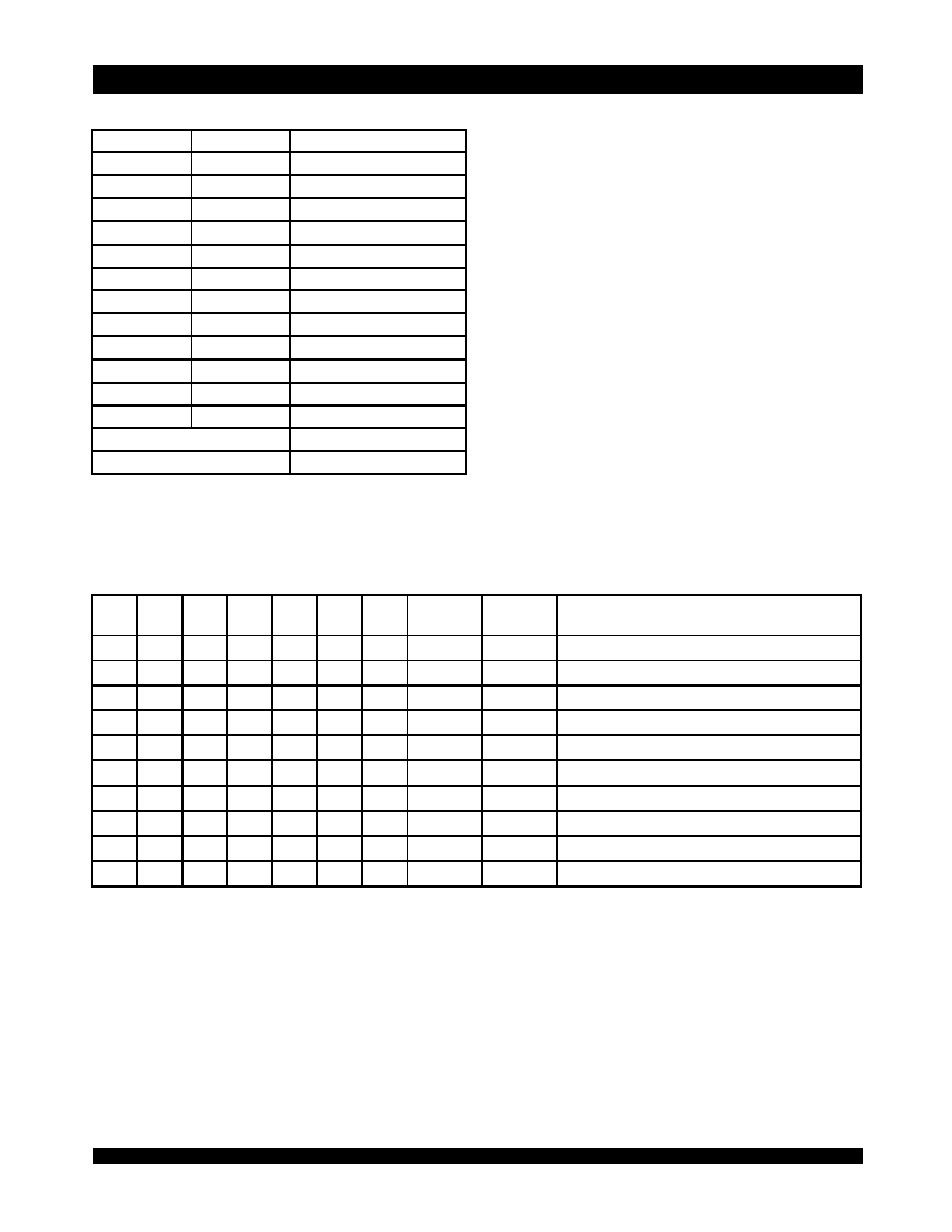
Pin Names
NOTES:
1. "H" = V
IH,
"L" = V
IL,
"X" = Don't Care.
2.
ADS, CNTEN, CNTRST = X.
3.
OE is an asynchronous input signal.
Truth Table IRead/Write and Enable Control
(1,2,3)
Left Port
Right Port
Names
CE
0L
,
CE
1L
CE
0R
,
CE
1R
Chip Enables
R/
W
L
R/
W
R
Read/Write Enable
OE
L
OE
R
Output Enable
A
0L
- A
13L
A
0R
- A
13R
Address
I/O
0L
- I/O
15L
I/O
0R
- I/O
15R
Data Input/Output
CLK
L
CLK
R
Clock
UB
L
UB
R
Upper Byte Select
LB
L
LB
R
Lower Byte Select
ADS
L
ADS
R
Address Strobe
CNTEN
L
CNTEN
R
Counter Enable
CNTRST
L
CNTRST
R
Counter Reset
FT/PIPE
L
FT/PIPE
R
Flow-Through/Pipeline
V
CC
Power
GND
Ground
3493 tbl 01
OE
CLK
CE
0
CE
1
UB
LB
R/
W
Upper
Byte
I/O
8-15
Lower B
yte
I/O
0-7
Mode
X
H
X
X
X
X
High-Z
High-Z
Deselected--Power Down
X
X
L
X
X
X
High-Z
High-Z
Deselected--Power Down
X
L
H
H
H
X
High-Z
High-Z
Both Bytes Deselected
X
L
H
L
H
L
D
IN
High-Z
Write to Upper Byte Only
X
L
H
H
L
L
High-Z
D
IN
Write to Lower Byte Only
X
L
H
L
L
L
D
IN
D
IN
Write to Both Bytes
L
L
H
L
H
H
D
OUT
High-Z
Read Upper Byte Only
L
L
H
H
L
H
High-Z
D
OUT
Read Lower Byte Only
L
L
H
L
L
H
D
OUT
D
OUT
Read Both Bytes
H
X
L
H
L
L
X
High-Z
High-Z
Outputs Disabled
3493 tbl 02
6.42
IDT709269S/L Preliminary
High-Speed 16K x 16 Synchronous Pipelined Dual-Port Static RAM Industrial and Commercial Temperature Ranges
4
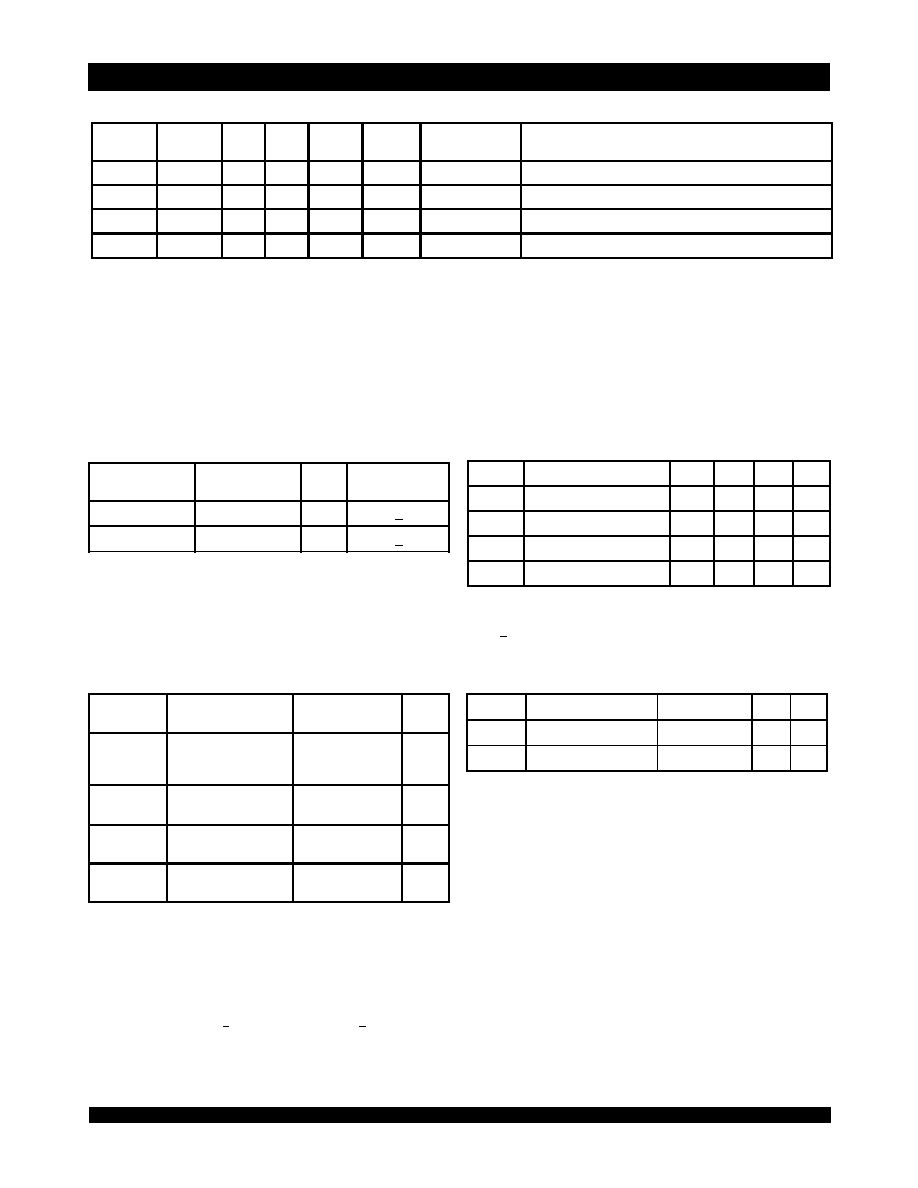
Recommended Operating
Temperature and Supply Voltage
(1,2)
Recommended DC Operating
Conditions
NOTES:
1. Stresses greater than those listed under ABSOLUTE MAXIMUM RATINGS may
cause permanent damage to the device. This is a stress rating only and functional
operation of the device at these or any other conditions above those indicated in the
operational sections of this specification is not implied. Exposure to absolute
maximum rating conditions for extended periods may affect reliability.
2. V
TERM
must not exceed V
cc
+ 10% for more than 25% of the cycle time or 10ns
maximum, and is limited to < 20mA for the period of V
TERM
> V
CC
+ 10%.
Absolute Maximum Ratings
(1)
N
OTES:
1. These parameters are determined by device characterization, but are not produc-
tion tested.
2. 3dV references the interpolated capacitance when the input and output switch from
0V to 3V or from 3V to 0V.
3. C
OUT
also references C
I/O
.
Capacitance
(T
A
= +25∞C, f = 1.0MH
z
)
NOTES:
1. V
TERM
must not exceed V
CC
+ 10%.
2. V
IL
> -1.5V for pulse width less than 10ns.
NOTES:
1. This is the parameter T
A
.
2. Industrial temperature: for specific speeds, packages and powers contact your
sales office.
Grade
Ambient
Temperature
GND
Vcc
Commercial
0
O
C to +70
O
C
0V
5.0V
+
10%
Industrial
-40
O
C to +85
O
C
0V
5.0V
+
10%
3493 tbl 04
Symbol
Parameter
Min.
Typ.
Max.
Unit
V
CC
Supply Voltage
4.5
5.0
5.5
V
GND
Ground
0
0
0
V
V
IH
Input High Voltage
2.2
____
6.0
(1)
V
V
IL
Input Low Voltage
-0.5
(2)
____
0.8
V
3493 tbl 05
Symbol
Rating
Commercial
& Industrial
Unit
V
TERM
(2)
Terminal Voltage
with Respect
to GND
-0.5 to +7.0
V
T
BIAS
Temperature
Under Bias
-55 to +125
o
C
T
STG
Storage
Temperature
-55 to +125
o
C
I
OUT
DC Output
Current
50
mA
3493 tbl 06
Symbol
Parameter
(1)
Conditions
(2)
Max.
Unit
C
IN
Input Capacitance
V
IN
= 3dV
9
pF
C
OUT
(3)
Output Capacitance
V
OUT
= 3dV
10
pF
3493 tbl 07
NOTES:
1. "H" = V
IH,
"L" = V
IL,
"X" = Don't Care.
2.
CE
0
,
LB
,
UB
, and
OE
= V
IL
; CE
1
and R/
W
= V
IH
.
3. Outputs configured in Flow-Through Output mode; if outputs are in Pipelined mode the data out will be delayed by one cycle.
4.
ADS
is independent of all other signals including
CE
0
, CE
1
,
UB
and
LB
.
5. The address counter advances if
CNTEN
= V
IL
on the rising edge of CLK, regardless of all other signals including
CE
0
, CE
1
,
UB
and
LB
.
TRUTH TABLE IIAddress Counter Control
(1,2)
Address
Previous
Address
CLK
ADS
CNTEN
CNTRST
I/O
(3)
Mode
X
X
H
H
L
D
I/O
(0)
Counter Reset to Address 0
An
X
L
(4)
H
H
D
I/O
(n)
External Address Utilized
X
An
H
H
H
D
I/O
(n)
External Address Blocked--Counter Disabled
X
An
H
L
(5)
H
D
I/O
(n+1)
Counter Enable--Internal Address Generation
3493 tbl 03
6.42
IDT709269S/L Preliminary
High-Speed 16K x 16 Synchronous Pipelined Dual-Port Static RAM Industrial and Commercial Temperature Ranges
5
NOTES:
1. At f = f
MAX
, address and control lines (except Output Enable) are cycling at the maximum frequency clock cycle of 1/t
CYC
, using "AC TEST CONDITIONS" at input levels of
GND to 3V.
2. f = 0 means no address, clock, or control lines change. Applies only to input at CMOS level standby.
3. Port "A" may be either left or right port. Port "B" is the opposite from port "A".
4. V
CC
= 5V, T
A
= 25∞C for Typ, and are not production tested. I
CC DC
(f=0)
= 150mA (Typ).
5.
CE
X
= V
IL
means
CE
0X
= V
IL
and CE
1X
= V
IH
CE
X
= V
IH
means
CE
0X
= V
IH
or CE
1X
= V
IL
CE
X
< 0.2V means
CE
0X
< 0.2V and CE
1X
> V
CC
- 0.2V
CE
X
> V
CC
- 0.2V means
CE
0X
> V
CC
- 0.2V or CE
1X
< 0.2V
"X" represents "L" for left port or "R" for right port.
6. 'X' in part number indicates power rating (S or L).
7. Industrial temperature: for specific speeds, packages and powers contact your sales office.
DC Electrical Characteristics Over the Operating
Temperature and Supply Voltage Range
(6,7)
(V
CC
= 5V ± 10%)
DC Electrical Characteristics Over the Operating
Temperature Supply Voltage Range
(V
CC
= 5.0V ± 10%)
N
OTE:
1.
At V
CC
< 2.0V input leakages are undefined.
Symbol
Parameter
Test Conditions
709269S/L
Unit
Min.
Max.
|I
LI
|
Input Leakage Current
(1)
V
CC
= 5.5V, V
IN
= 0V to V
CC
___
10
µ A
|I
LO
|
Output Leakage Current
CE
0
= V
IH
or CE
1
= V
IL
, V
OUT
= 0V to V
CC
___
10
µ A
V
OL
Output Low Voltage
I
OL
= +4mA
___
0.4
V
V
OH
Output High Voltage
I
OH
= -4mA
2.4
___
V
3493 tbl 08
709269X9
Com'l Only
709269X12
Com'l Only
709269X15
Com'l Only
Symbol
Parameter
Test Condition
Version
Typ.
(4)
Max.
Typ.
(4)
Max.
Typ.
(4)
Max.
Unit
I
CC
Dynamic Operating
Current
(Both Ports Active)
CE
L
and
CE
R
= V
IL
Outputs Open
f = f
MAX
(1)
COM'L
S
L
210
210
390
350
200
200
345
305
190
190
325
285
mA
IND
S
L
____
____
____
____
____
____
____
____
____
____
____
____
I
SB1
Standby Current
(Both Ports - TTL
Level Inputs)
CE
L
=
CE
R
= V
IH
f = f
MAX
(1)
COM'L
S
L
50
50
135
115
50
50
110
90
50
50
110
90
mA
IND
S
L
____
____
____
____
____
____
____
____
____
____
____
____
I
SB2
Standby Current
(One Port - TTL
Level Inputs)
CE
"A"
= V
IL
and
CE
"B"
= V
IH
(3)
Active Port Outputs
Open,
f=f
MAX
(3)
COM'L
S
L
140
140
270
240
130
130
230
200
120
120
220
190
mA
IND
S
L
____
____
____
____
____
____
____
____
____
____
____
____
I
SB3
Full Standby Current
(Both Ports -
CMOS Level Inputs)
Both Ports
CE
R
and
CE
L
> V
CC
- 0.2V
V
IN
> V
CC
- 0.2V or
V
IN
< 0.2V, f = 0
(2)
COM'L
S
L
1.0
0.2
15
5
1.0
0.2
15
5
1.0
0.2
15
5
mA
IND
S
L
____
____
____
____
____
____
____
____
____
____
____
____
I
SB4
Full Standby Current
(One Port -
CMOS Level Inputs)
CE
"A"
< 0.2V and
CE
"B"
> V
CC
- 0.2V
(5)
V
IN
> V
CC
- 0.2V or
V
IN
< 0.2V, Active Port
Outputs Open, f = f
MAX
(1)
COM'L
S
L
130
130
245
225
120
120
205
185
110
110
195
175
mA
IND
S
L
____
____
____
____
____
____
____
____
____
____
____
____
3493 tbl 09