 | –≠–ª–µ–∫—Ç—Ä–æ–Ω–Ω—ã–π –∫–æ–º–ø–æ–Ω–µ–Ω—Ç: 70V3569 | –°–∫–∞—á–∞—Ç—å:  PDF PDF  ZIP ZIP |

©2001 Integrated Device Technology, Inc.
APRIL 2001
DSC 4831/8
1
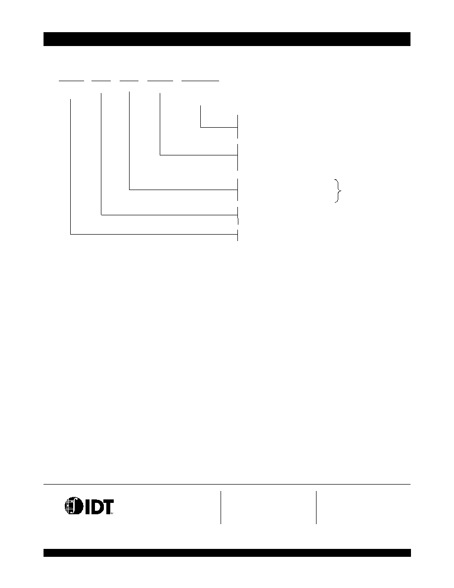
Functional Block Diagram
Features:
x
True Dual-Port memory cells which allow simultaneous
access of the same memory location
x
High-speed clock to data access
≠ Commercial: 4.2/5/6ns (max.)
≠ Industrial: 5/6ns (max)
x
Pipelined output mode
x
Counter enable and reset features
x
Dual chip enables allow for depth expansion without
additional logic
x
Full synchronous operation on both ports
≠ 7.5ns cycle time, 133MHz operation (9.6 Gbps bandwidth)
≠ Fast 4.2ns clock to data out
≠ 1.8ns setup to clock and 0.7ns hold on all control, data, and
address inputs @ 133MHz
≠ Data input, address, byte enable and control registers
≠ Self-timed write allows fast cycle time
x
Separate byte controls for multiplexed bus and bus
matching compatibility
x
LVTTL- compatible, single 3.3V (±150mV) power supply for
core
x
LVTTL- compatible, selectable 3.3V (±150mV)/2.5V (±125mV)
power supply for I/Os and control signals on each port
x
Industrial temperature range (-40∞C to +85∞C) is
available for selected speeds
x
Available in a 208-pin Plastic Quad Flatpack (PQFP),
208-ball fine-pitch Ball Grid Array, and 256-pin Ball
Grid Array
HIGH-SPEED 3.3V 16K x 36
SYNCHRONOUS PIPELINED
DUAL-PORT STATIC RAM
WITH 3.3V OR 2.5V INTERFACE
IDT70V3569S
CNTRST
R
Counter/
Address
Reg.
A
13R
A
0R
Counter/
Address
Reg.
CNTEN
R
ADS
R
CNTEN
L
ADS
L
CNTRST
L
Dout0-8_L
Dout9-17_L
Dout18-26_L
Dout27-35_L
Dout0-8_R
Dout9-17_R
Dout18-26_R
Dout27-35_R
B
W
0
L
B
W
1
L
B
W
2
L
B
W
3
L
B
W
3
R
B
W
2
R
B
W
1
R
B
W
0
R
I/O
0L
- I/O
35L
A
13L
A
0L
I/O
0R
- I/O
35R
Din_L
ADDR_L
Din_R
ADDR_R
OE
R
OE
L
4831 tbl 01
BE
3L
BE
2L
BE
1L
BE
0L
R/
W
L
CE
0L
BE
3R
BE
2R
BE
1R
BE
0R
R/
W
R
CE
0R
CE
1R
CE
1L
16K x 36
MEMORY
ARRAY
CLK
R
CLK
L
,

6.42
IDT70V3569S
High-Speed 16K x 36 Dual-Port Synchronous Pipelined Static RAM Industrial and Commercial Temperature Ranges
2
Description:
The IDT70V3569 is a high-speed 16K x 36 bit synchronous Dual-Port
RAM. The memory array utilizes Dual-Port memory cells to allow
simultaneous access of any address from both ports. Registers on control,
data, and address inputs provide minimal setup and hold times. The timing
latitude provided by this approach allows systems to be designed with very
short cycle times. With an input data register, the IDT70V3569 has been
optimized for applications having unidirectional or bidirectional data flow
in bursts. An automatic power down feature, controlled by
CE
0
and CE
1,
permits the on-chip circuitry of each port to enter a very low standby power
mode.
The 70V3569 can support an operating voltage of either 3.3V or
2.5V on one or both ports, controllable by the OPT pins. The power
supply for the core of the device (V
DD
) remains at 3.3V.
Pin Configuration
(1,2,3,4)
NOTES:
1. All V
DD
pins must be connected to 3.3V power supply.
2. All V
DDQ
pins must be connected to appropriate power supply: 3.3V if OPT pin for that port is set to V
IH
(3.3V), and 2.5V if OPT pin for that port is
set to V
IL
(0V).
3. All V
SS
pins must be connected to ground supply.
4. Package body is approximately 15mm x 15mm x 1.4mm, with 0.8mm ball pitch.
5. This package code is used to reference the package diagram.
6. This text does not indicate orientation of the actual part-marking.
A17
V
SS
B17
I/O
15R
C17
V
SS
D17
I/O
14R
E16
V
SS
E17
I/O
13L
D16
I/O
14L
C16
I/O
15L
B16
I/O
16L
A16
I/O
17L
A15
OPT
L
B15
V
DDQR
C15
I/O
16R
D15
V
DDQL
E15
I/O
13R
E14
I/O
12L
D14
I/O
17R
D13
V
DD
C12
A
6L
C14
V
DD
B14
V
SS
A14
A
0L
A12
CNTEN
L
B12
A
5L
C11
R/
W
L
D12
A
3L
D11
CNTRST
L
C10
V
SS
B11
ADS
L
A11
CLK
L
D8
BE
0L
C8
BE
3L
A9
BE
1L
D9
V
DD
C9
CE
1L
B9
CE
0L
D10
OE
L
C7
A
10L
B8
BE
2L
A8
A
8L
B13
A
1L
A13
A
4L
A10
V
DD
D7
A
7L
B7
A
9L
B6
A
13L
C6
NC
D6
A
11L
B5
NC
C5
NC
D5
NC
B4
V
SS
C4
V
DD
D4
I/O
20L
B3
I/O
18R
C3
V
DDQR
D3
I/O
21L
D2
V
SS
C2
I/O
19R
B2
V
SS
B1
I/O
20R
C1
V
DDQL
D1
I/O
22L
E1
I/O
23L
E2
I/O
22R
E3
V
DDQR
E4
I/O
21R
F1
V
DDQL
F2
I/O
23R
F3
I/O
24L
F4
V
SS
G1
I/O
26L
G2
V
SS
G3
I/O
25L
G4
I/O
24R
H1
V
DD
H2
I/O
26R
H3
V
DDQR
H4
I/O
25R
J1
V
DDQL
J2
V
DD
J3
V
SS
J4
V
SS
K1
I/O
28R
K2
V
SS
K3
I/O
27R
K4
V
SS
L1
I/O
29R
L2
I/O
28L
L3
V
DDQR
L4
I/O
27L
M1
V
DDQL
M2
I/O
29L
M3
I/O
30R
M4
V
SS
N1
I/O
31L
N2
V
SS
N3
I/O
31R
N4
I/O
30L
P1
I/O
32R
P2
I/O
32L
P3
V
DDQR
P4
I/O
35R
R1
V
SS
R2
I/O
33L
R3
I/O
34R
R4
NC
T1
I/O
33R
T2
I/O
34L
T3
V
DDQL
T4
V
SS
U1
V
SS
U2
I/O
35L
U3
V
DD
U4
NC
P5
NC
R5
NC
U6
A
11R
P12
CNTEN
R
P8
A
8R
U10
OE
R
P9
BE
1R
R8
BE
2R
T8
BE
3R
U9
V
DD
P10
V
DD
T11
R/
W
R
U8
BE
0R
P11
CLK
R
R12
A
5R
T12
A
6R
U12
A
3R
P13
A
4R
P7
A
12R
R13
A
1R
T13
A
2R
U13
A
0R
R6
A
13R
T5
NC
U7
A
7R
U14
V
DD
T14
V
SS
R14
V
SS
P14
I/O
2L
P15
I/O
3L
R15
V
DDQL
T15
I/O
0R
U15
OPT
R
U16
I/O
0L
U17
I/O
1L
T16
V
SS
T17
I/O
2R
R17
V
DDQR
R16
I/O
1R
P17
I/O
4L
P16
V
SS
N17
I/O
5L
N16
I/O
4R
N15
V
DDQL
N14
I/O
3R
M17
V
DDQR
M16
I/O
5R
M15
I/O
6L
M14
V
SS
L17
I/O
8L
L16
V
SS
L15
I/O
7L
L14
I/O
6R
K17
V
SS
K16
I/O
8R
K15
V
DDQL
K14
I/O
7R
J17
V
DDQR
J16
V
SS
J15
V
DD
J14
V
SS
H17
I/O
10R
H16
V
SS
H15
IO
9R
H14
V
DD
G17
I/O
11R
G16
I/O
10L
G15
V
DDQL
G14
I/O
9L
F17
V
DDQR
F16
I/O
11L
F14
V
SS
70V3569BF
BF-208
(5)
208-Pin fpBGA
Top View
(6)
F15
I/O
12R
R9
CE
0R
R11
ADS
R
T6
NC
T9
CE
1R
B10
V
SS
C13
A
2L
P6
NC
R10
V
SS
R7
A
9R
T10
V
SS
T7
A
10R
U5
NC
4831 drw 02c
,
A7
A
12L
A5
NC
A4
NC
A3
V
SS
A2
IO
18L
A1
IO
19L
A6
NC

6.42
IDT70V3569S
High-Speed 16K x 36 Dual-Port Synchronous Pipelined Static RAM Industrial and Commercial Temperature Ranges
3
Pin Configuration
(1,2,3,4)
(con't.)
NOTES:
1. All V
DD
pins must be connected to 3.3V power supply.
2. All V
DDQ
pins must be connected to appropriate power supply: 3.3V if OPT pin for that port is set to V
IH
(3.3V), and 2.5V if OPT pin for that port is
set to V
IL
(0V).
3. All V
SS
pins must be connected to ground supply.
4. Package body is approximately 17mm x 17mm x 1.4mm, with 1.0mm ball-pitch.
5. This package code is used to reference the package diagram.
6. This text does not indicate orientation of the actual part-marking.
70V3569BC
BC-256
(5)
256-Pin BGA
Top View
(6)
E16
I/O
14R
D16
I/O
16R
C16
I/O
16L
B16
NC
A16
NC
A15
NC
B15
I/O
17L
C15
I/O
17R
D15
I/O
15L
E15
I/O
14L
E14
I/O
13L
D14
I/O
15R
D13
V
DD
C12
A
6L
C14
OPT
L
B14
V
DD
A14
A
0L
A12
A
5L
B12
A
4L
C11
ADS
L
D12
V
DDQR
D11
V
DDQR
C10
CLK
L
B11
CNTRST
L
A11
CNTEN
L
D8
V
DDQR
C8
BE
1L
A9
CE
1L
D9
V
DDQL
C9
BE
0L
B9
CE
0L
D10
V
DDQL
C7
A
7L
B8
BE
3L
A8
BE
2L
B13
A
1L
A13
A
2L
A10
OE
L
D7
V
DDQR
B7
A
9L
A7
A
8L
B6
A
12L
C6
A
10L
D6
V
DDQL
A5
NC
B5
NC
C5
A
13L
D5
V
DDQL
A4
NC
B4
NC
C4
NC
D4
V
DD
A3
NC
B3
NC
C3
V
SS
D3
I/O
20L
D2
I/O
19R
C2
I/O
19L
B2
NC
A2
NC
A1
NC
B1
I/O
18L
C1
I/O
18R
D1
I/O
20R
E1
I/O
21R
E2
I/O
21L
E3
I/O
22L
E4
V
DDQL
F1
I/O
23L
F2
I/O
22R
F3
I/O
23R
F4
V
DDQL
G1
I/O
24R
G2
I/O
24L
G3
I/O
25L
G4
V
DDQR
H1
I/O
26L
H2
I/O
25R
H3
I/O
26R
H4
V
DDQR
J1
I/O
27L
J2
I/O
28R
J3
I/O
27R
J4
V
DDQL
K1
I/O
29R
K2
I/O
29L
K3
I/O
28L
K4
V
DDQL
L1
I/O
30L
L2
I/O
31R
L3
I/O
30R
L4
V
DDQR
M1
I/O
32R
M2
I/O
32L
M3
I/O
31L
M4
V
DDQR
N1
I/O
33L
N2
I/O
34R
N3
I/O
33R
N4
V
DD
P1
I/O
35R
P2
I/O
34L
P3
NC
P4
NC
R1
I/O
35L
R2
NC
R3
NC
R4
NC
T1
NC
T2
NC
T3
NC
T4
NC
P5
A
13R
R5
NC
P12
A
6R
P8
BE
1R
P9
BE
0R
R8
BE
3R
T8
BE
2R
P10
CLK
R
T11
CNTEN
R
P11
ADS
R
R12
A
4R
T12
A
5R
P13
A
3R
P7
A
7R
R13
A
1R
T13
A
2R
R6
A
12R
T5
NC
T14
A
0R
R14
OPT
R
P14
I/O
0L
P15
I/O
0R
R15
NC
T15
NC
T16
NC
R16
NC
P16
I/O
1L
N16
I/O
2R
N15
I/O
1R
N14
I/O
2L
M16
I/O
4L
M15
I/O
3L
M14
I/O
3R
L16
I/O
5R
L15
I/O
4R
L14
I/O
5L
K16
I/O
7L
K15
I/O
6L
K14
I/O
6R
J16
I/O
8L
J15
I/O
7R
J14
I/O
8R
H16
I/O
10R
H15
IO
9L
H14
I/O
9R
G16
I/O
11R
G15
I/O
11L
G14
I/O
10L
F16
I/O
12L
F14
I/O
12R
F15
I/O
13R
R9
CE
0R
R11
CNTRST
R
T6
A
11R
T9
CE
1R
A6
A
11L
B10
R/
W
L
C13
A
3L
P6
A
10R
R10
R/
W
R
R7
A
9R
T10
OE
R
T7
A
8R
,
E5
V
DD
E6
V
DD
E7
V
SS
E8
V
SS
E9
V
SS
E10
V
SS
E11
V
DD
E12
V
DD
E13
V
DDQR
F5
V
DD
F6
V
SS
F8
V
SS
F9
V
SS
F10
V
SS
F12
V
DD
F13
V
DDQR
G5
V
SS
G6
V
SS
G7
V
SS
G8
V
SS
G9
V
SS
G10
V
SS
G11
V
SS
G12
V
SS
G13
V
DDQL
H5
V
SS
H6
V
SS
H7
V
SS
H8
V
SS
H9
V
SS
H10
V
SS
H11
V
SS
H12
V
SS
H13
V
DDQL
J5
V
SS
J6
V
SS
J7
V
SS
J8
V
SS
J9
V
SS
J10
V
SS
J11
V
SS
J12
V
SS
J13
V
DDQR
K5
V
SS
K6
V
SS
K7
V
SS
K8
V
SS
L5
V
DD
L6
V
SS
L7
V
SS
L8
V
SS
M5
V
DD
M6
V
DD
M7
V
SS
M8
V
SS
N5
V
DDQR
N6
V
DDQR
N7
V
DDQL
N8
V
DDQL
K9
V
SS
K10
V
SS
K11
V
SS
K12
V
SS
L9
V
SS
L10
V
SS
L11
V
SS
L12
V
DD
M9
V
SS
M10
V
SS
M11
V
DD
M12
V
DD
N9
V
DDQR
N10
V
DDQR
N11
V
DDQL
N12
V
DDQL
K13
V
DDQR
L13
V
DDQL
M13
V
DDQL
N13
V
DD
F7
V
SS
F11
V
SS
4831 drw 02d
,

6.42
IDT70V3569S
High-Speed 16K x 36 Dual-Port Synchronous Pipelined Static RAM Industrial and Commercial Temperature Ranges
4
Pin Configuration
(1,2,3,4)
(con't.)
NOTES:
1. All V
DD
pins must be connected to 3.3V power supply.
2. All V
DDQ
pins must be connected to appropriate power supply: 3.3V if OPT pin for that port is set to V
IH
(3.3V), and 2.5V if OPT pin for that port is
set to V
IL
(0V).
3. All V
SS
pins must be connected to ground supply.
4. Package body is approximately 28mm x 28mm x 3.5mm.
5. This package code is used to reference the package diagram.
6. This text does not indicate orientation of the actual part-marking.
1
2
3
4
5
6
7
8
9
10
11
12
13
14
15
16
17
18
19
20
21
22
23
24
25
26
27
28
29
30
31
32
33
34
35
36
37
38
39
40
41
42
43
44
45
46
47
48
49
50
51
52
5
3
5
4
5
5
5
6
5
7
5
8
5
9
6
0
6
1
6
2
6
3
6
4
6
5
6
6
6
7
6
8
6
9
7
0
7
1
7
2
7
3
7
4
7
5
7
6
7
7
7
8
7
9
8
0
8
1
8
2
8
3
8
4
8
5
8
6
8
7
8
8
8
9
9
0
9
1
9
2
9
3
9
4
9
5
9
6
9
7
9
8
9
9
1
0
0
1
0
1
1
0
2
1
0
3
1
0
4
156
155
154
153
152
151
150
149
148
147
146
145
144
143
142
141
140
139
138
137
136
135
134
133
132
131
130
129
128
127
126
125
124
123
122
121
120
119
118
117
116
115
114
113
112
111
110
109
108
107
106
105
2
0
8
2
0
7
2
0
6
2
0
5
2
0
4
2
0
3
2
0
2
2
0
1
2
0
0
1
9
9
1
9
8
1
9
7
1
9
6
1
9
5
1
9
4
1
9
3
1
9
2
1
9
1
1
9
0
1
8
9
1
8
8
1
8
7
1
8
6
1
8
5
1
8
4
1
8
3
1
8
2
1
8
1
1
8
0
1
7
9
1
7
8
1
7
7
1
7
6
1
7
5
1
7
4
1
7
3
1
7
2
1
7
1
1
7
0
1
6
9
1
6
8
1
6
7
1
6
6
1
6
5
1
6
4
1
6
3
1
6
2
1
6
1
1
6
0
1
5
9
1
5
8
1
5
7
70V3569DR
DR-208
(5)
208-Pin PQFP
Top View
(6)
I/O
19L
I/O
19R
I/O
20L
I/O
20R
V
DDQL
V
SS
I/O
21L
I/O
21R
I/O
22L
I/O
22R
V
DDQR
V
SS
I/O
23L
I/O
23R
I/O
24L
I/O
24R
V
DDQL
V
SS
I/O
25L
I/O
25R
I/O
26L
I/O
26R
V
DDQR
V
SS
V
DD
V
DD
V
SS
V
SS
V
DDQL
V
SS
I/O
27R
I/O
27L
I/O
28R
I/O
28L
V
DDQR
V
SS
I/O
29R
I/O
29L
I/O
30R
I/O
30L
V
DDQL
V
SS
I/O
31R
I/O
31L
I/O
32R
I/O
32L
V
DDQR
V
SS
I/O
33R
I/O
33L
I/O
34R
I/O
34L
V
S
S
V
D
D
Q
L
I
/
O
3
5
R
I
/
O
3
5
L
V
D
D
V
S
S
N
C
N
C
N
C
N
C
N
C
N
C
N
C
N
C
A
1
3
R
A
1
2
R
A
1
1
R
A
1
0
R
A
9
R
A
8
R
A
7
R
B
E
3
R
B
E
2
R
B
E
1
R
B
E
0
R
C
E
1
R
C
E
0
R
V
D
D
V
D
D
V
S
S
V
S
S
C
L
K
R
O
E
R
R
/
W
R
A
D
S
R
C
N
T
E
N
R
C
N
T
R
S
T
R
A
6
R
A
5
R
A
4
R
A
3
R
A
2
R
A
1
R
A
0
R
V
D
D
V
S
S
V
S
S
O
P
T
R
I
/
O
0
L
I
/
O
0
R
V
D
D
Q
L
V
S
S
I/O
16L
I/O
16R
I/O
15L
I/O
15R
V
SS
V
DDQL
I/O
14L
I/O
14R
I/O
13L
I/O
13R
V
SS
V
DDQR
I/O
12L
I/O
12R
I/O
11L
I/O
11R
V
SS
V
DDQL
I/O
10L
I/O
10R
I/O
9L
I/O
9R
V
SS
V
DDQR
V
DD
V
DD
V
SS
V
SS
V
SS
V
DDQL
I/O
8R
I/O
8L
I/O
7R
I/O
7L
V
SS
V
DDQR
I/O
6R
I/O
6L
I/O
5R
I/O
5L
V
SS
V
DDQL
I/O
4R
I/O
4L
I/O
3R
I/O
3L
V
SS
V
DDQR
I/O
2R
I/O
2L
I/O
1R
I/O
1L
V
S
S
V
D
D
Q
R
I
/
O
1
8
R
I
/
O
1
8
L
V
S
S
V
D
D
V
S
S
N
C
N
C
N
C
N
C
N
C
N
C
N
C
A
1
3
L
A
1
2
L
A
1
1
L
A
1
0
L
A
9
L
A
8
L
A
7
L
B
E
3
L
B
E
2
L
B
E
1
L
B
E
0
L
C
E
1
L
C
E
0
L
V
D
D
V
D
D
V
S
S
V
S
S
C
L
K
L
O
E
L
R
/
W
L
A
D
S
L
C
N
T
E
N
L
C
N
T
R
S
T
L
A
6
L
A
5
L
A
4
L
A
3
L
A
2
L
A
1
L
A
0
L
V
D
D
V
D
D
V
S
S
O
P
T
L
I
/
O
1
7
L
I
/
O
1
7
R
V
D
D
Q
R
V
S
S
4831 drw 02a

6.42
IDT70V3569S
High-Speed 16K x 36 Dual-Port Synchronous Pipelined Static RAM Industrial and Commercial Temperature Ranges
5
NOTES:
1. "H" = V
IH,
"L" = V
IL,
"X" = Don't Care.
2.
ADS, CNTEN, CNTRST = V
IH
.
3. OE is an asynchronous input signal.
4. It is possible to read or write any combination of bytes during a given access. A few representative samples have been illustrated here.
Truth Table IRead/Write and Enable Control
(1,2,3,4)
Pin Names
Left Port
Right Port
Names
CE
0L
,
CE
1L
CE
0R
,
CE
1R
Chip Enables
R/W
L
R/W
R
Read/Write Enable
OE
L
OE
R
Output Enable
A
0L
- A
13L
A
0R
- A
13R
Address
I/O
0L
- I/O
35L
I/O
0R
- I/O
35R
Data Input/Output
CLK
L
CLK
R
Clock
ADS
L
ADS
R
Address Strobe Enable
CNTEN
L
CNTEN
R
Counter Enable
CNTRST
L
CNTRST
R
Counter Reset
BE
0L
- BE
3L
BE
0R
- BE
3R
Byte Enables (9-bit bytes)
V
DDQL
V
DDQR
Power (I/O Bus)
(3.3V or 2.5V)
(1)
OPT
L
OPT
R
Option for selection V
DDQX
(1,2)
V
DD
Power
(3.3V)
(1)
V
SS
Ground
(0V)
4831 tbl 01
OE
CLK
CE
0
CE
1
BE
3
BE
2
BE
1
BE
0
R/
W
Byte 3
I/O
27-35
Byte 2
I/O
18-26
Byte 1
I/O
9-17
Byte 0
I/O
0-8
MODE
X
H
X
X
X
X
X
X
High-Z
High-Z
High-Z
High-Z
Deselected≠Power Down
X
X
L
X
X
X
X
X
High-Z
High-Z
High-Z
High-Z
Deselected≠Power Down
X
L
H
H
H
H
H
X
High-Z
High-Z
High-Z
High-Z
All Bytes Deselected
X
L
H
H
H
H
L
L
High-Z
High-Z
High-Z
D
IN
Write to Byte 0 Only
X
L
H
H
H
L
H
L
High-Z
High-Z
D
IN
High-Z
Write to Byte 1 Only
X
L
H
H
L
H
H
L
High-Z
D
IN
High-Z
High-Z
Write to Byte 2 Only
X
L
H
L
H
H
H
L
D
IN
High-Z
High-Z
High-Z
Write to Byte 3 Only
X
L
H
H
H
L
L
L
High-Z
High-Z
D
IN
D
IN
Write to Lower 2 Bytes Only
X
L
H
L
L
H
H
L
D
IN
D
IN
High-Z
High-Z
Write to Upper 2 bytes Only
X
L
H
L
L
L
L
L
D
IN
D
IN
D
IN
D
IN
Write to All Bytes
L
L
H
H
H
H
L
H
High-Z
High-Z
High-Z
D
OUT
Read Byte 0 Only
L
L
H
H
H
L
H
H
High-Z
High-Z
D
OUT
High-Z
Read Byte 1 Only
L
L
H
H
L
H
H
H
High-Z
D
OUT
High-Z
High-Z
Read Byte 2 Only
L
L
H
L
H
H
H
H
D
OUT
High-Z
High-Z
High-Z
Read Byte 3 Only
L
L
H
H
H
L
L
H
High-Z
High-Z
D
OUT
D
OUT
Read Lower 2 Bytes Only
L
L
H
L
L
H
H
H
D
OUT
D
OUT
High-Z
High-Z
Read Upper 2 Bytes Only
L
L
H
L
L
L
L
H
D
OUT
D
OUT
D
OUT
D
OUT
Read All Bytes
H
L
H
L
L
L
L
X
High-Z
High-Z
High-Z
High-Z
Outputs Disabled
4831 tbl 02
NOTES:
1. V
DD
, OPT
X
, and V
DDQX
must be set to appropriate operating levels prior to
applying inputs on the I/Os and controls for that port.
2. OPT
X
selects the operating voltage levels for the I/Os and controls on that port.
If OPT
X
is set to VIH (3.3V), then that port's I/Os and controls will operate at 3.3V
levels and V
DDQX
must be supplied at 3.3V. If OPT
X
is set to VIL (0V), then that
port's I/Os and controls will operate at 2.5V levels and V
DDQX
must be supplied
at 2.5V. The OPT pins are independent of one another--both ports can operate
at 3.3V levels, both can operate at 2.5V levels, or either can operate at 3.3V
with the other at 2.5V.

6.42
IDT70V3569S
High-Speed 16K x 36 Dual-Port Synchronous Pipelined Static RAM Industrial and Commercial Temperature Ranges
6
Recommended Operating
Temperature and Supply Voltage
(1,2)
Recommended DC Operating
Conditions with V
DDQ
at 2.5V
Absolute Maximum Ratings
(1)
Truth Table IIAddress Counter Control
(1,2)
NOTES:
1. "H" = V
IH,
"L" = V
IL,
"X" = Don't Care.
2. Read and write operations are controlled by the appropriate setting of R/
W, CE
0
, CE
1
,
BEn and OE.
3. Outputs are in Pipelined mode: the data out will be delayed by one cycle.
4.
ADS and CNTRST are independent of all other memory control signals including CE
0
, CE
1
and
BEn
5. The address counter advances if
CNTEN = V
IL
on the rising edge of CLK, regardless of all other memory control signals including
CE
0
, CE
1
,
BEn.
NOTES:
1. Stresses greater than those listed under ABSOLUTE MAXIMUM RATINGS may
cause permanent damage to the device. This is a stress rating only and functional
operation of the device at these or any other conditions above those indicated
in the operational sections of this specification is not implied. Exposure to absolute
maximum rating conditions for extended periods may affect reliability.
2. V
TERM
must not exceed V
DD
+ 150mV for more than 25% of the cycle time or
4ns maximum, and is limited to < 20mA for the period of V
TERM
> V
DD
+ 150mV.
NOTES:
1. Industrial temperature: for specific speeds, packages and powers contact your
sales office.
2. This is the parameter T
A
. This is the "instant on" case temperature.
Address
Previous
Address
Addr
Used
CLK
(6)
ADS
CNTEN
CNTRST
I/O
(3)
MODE
X
X
0
X
X
L
(4)
D
I/O
(0)
Counter Reset to Address 0
An
X
An
L
(4)
X
H
D
I/O
(n)
External Address Used
An
Ap
Ap
H
H
H
D
I/O
(p)
External Address Blocked--Counter disabled (Ap reused)
X
Ap
Ap + 1
H
L
(5)
H
D
I/O
(p+1)
Counter Enabled--Internal Address generation
4831 tbl 03
Grade
Ambient
Temperature
GND
V
DD
Commercial
0
O
C to +70
O
C
0V
3.3V
+
150mV
Industrial
-40
O
C to +85
O
C
0V
3.3V
+
150mV
4831 tbl 04
Symbol
Parameter
Min.
Typ.
Max.
Unit
V
DD
Core Supply Voltage
3.15
3.3
3.45
V
V
DDQ
I/O Supply Voltage
(3)
2.375
2.5
2.625
V
V
SS
Ground
0
0
0
V
V
IH
Input High Voltage
(3)
(Address & Control Inputs)
1.7
____
V
DDQ
+ 125mV
(2)
V
V
IH
Input High Voltage - I/O
(3)
1.7
____
V
DDQ
+ 125mV
(2)
V
V
IL
Input Low Voltage
-0.3
(1)
____
0.7
V
4831 tbl 05a
Symbol
Rating
Commercial
& Industrial
Unit
V
TERM
(2)
Terminal Voltage
with Respect to
GND
-0.5 to +4.6
V
T
BIAS
Temperature
Under Bias
-55 to +125
o
C
T
STG
Storage
Temperature
-65 to +150
o
C
I
OUT
DC Output Current
50
mA
4831 tbl 06
NOTES:
1. V
IL >
-1.5V for pulse width less than 10 ns.
2. V
TERM
must not exceed V
DDQ
+ 125mV.
3. To select operation at 2.5V levels on the I/Os and controls of a given port, the
OPT pin for that port must be set to V
IL
(0V), and V
DDQX
for that port must be
supplied as indicated above.
NOTES:
1. V
IL >
-1.5V for pulse width less than 10 ns.
2. V
TERM
must not exceed V
DDQ
+ 150mV.
3. To select operation at 3.3V levels on the I/Os and controls of a given port, the
OPT pin for that port must be set to V
IH
(3.3V), and V
DDQX
for that port must be
supplied as indicated above.
Recommended DC Operating
Conditions with V
DDQ
at 3.3V
Symbol
Parameter
Min.
Typ.
Max.
Unit
V
DD
Core Supply Voltage
3.15
3.3
3.45
V
V
DDQ
I/O Supply Voltage
(3)
3.15
3.3
3.45
V
V
SS
Ground
0
0
0
V
V
IH
Input High Voltage
(Address & Control Inputs)
(3)
2.0
____
V
DDQ
+ 150mV
(2)
V
V
IH
Input High Voltage - I/O
(3)
2.0
____
V
DDQ
+ 150mV
(2)
V
V
IL
Input Low Voltage
-0.3
(1)
____
0.8
V
4831 tbl 05b

6.42
IDT70V3569S
High-Speed 16K x 36 Dual-Port Synchronous Pipelined Static RAM Industrial and Commercial Temperature Ranges
7
DC Electrical Characteristics Over the Operating
Temperature and Supply Voltage Range
(V
DD
= 3.3V ± 150mV)
NOTE:
1. At V
DD
< - 2.0V input leakages are undefined.
2. V
DDQ
is selectable (3.3V/2.5V) via OPT pins. Refer to p.4 for details.
Symbol
Parameter
Test Conditions
70V3569S
Unit
Min.
Max.
|I
LI
|
Input Leakage Current
(1)
V
DDQ
= Max., V
IN
= 0V to V
DDQ
___
10
µ A
|I
LO
|
Output Leakage Current
CE
0
= V
IH
or CE
1
= V
IL
, V
OUT
= 0V to V
DDQ
___
10
µ A
V
OL
(3.3V)
Output Low Voltage
(2)
I
OL
= +4mA, V
DDQ
= Min.
___
0.4
V
V
OH
(3.3V)
Output High Voltage
(2)
I
OH
= -4mA, V
DDQ
= Min.
2.4
___
V
V
OL
(2.5V)
Output Low Voltage
(2)
I
OL
= +2mA, V
DDQ
= Min.
___
0.4
V
V
OH
(2.5V)
Output High Voltage
(2)
I
OH
= -2mA, V
DDQ
= Min.
2.0
___
V
4831 tbl 08
NOTES:
1. These parameters are determined by device characterization, but are not
production tested.
2. 3dV references the interpolated capacitance when the input and output switch
from 0V to 3V or from 3V to 0V.
3. C
OUT
also references C
I/O
.
Capacitance
(1)
(T
A
= +25∞C, F = 1.0MH
Z
) PQFP ONLY
Symbol
Parameter
Conditions
(2)
Max.
Unit
C
IN
Input Capacitance
V
IN
= 3dV
8
pF
C
OUT
(3)
Output Capacitance
V
OUT
= 3dV
10.5
pF
4831 tbl 07

6.42
IDT70V3569S
High-Speed 16K x 36 Dual-Port Synchronous Pipelined Static RAM Industrial and Commercial Temperature Ranges
8
DC Electrical Characteristics Over the Operating
Temperature and Supply Voltage Range
(3)
(V
DD
= 3.3V ± 150mV)
NOTES:
1. At f = f
MAX
, address and control lines (except Output Enable) are cycling at the maximum frequency clock cycle of 1/t
CYC
, using "AC TEST CONDITIONS" at input
levels of GND to 3V.
2. f = 0 means no address, clock, or control lines change. Applies only to input at CMOS level standby.
3. Port "A" may be either left or right port. Port "B" is the opposite from port "A".
4. V
DD
= 3.3V, T
A
= 25∞C for Typ, and are not production tested. I
DD DC
(f=0)
= 120mA (Typ).
5.
CE
X
= V
IL
means
CE
0X
= V
IL
and CE
1X
= V
IH
CE
X
= V
IH
means
CE
0X
= V
IH
or CE
1X
= V
IL
CE
X
< 0.2V means
CE
0X
< 0.2V and CE
1X
> V
CC
- 0.2V
CE
X
> V
CC
- 0.2V means
CE
0X
> V
CC
- 0.2V or CE
1X
- 0.2V
"X" represents "L" for left port or "R" for right port.
70V3569S4
Com 'l Only
70V3569S5
Com 'l
& Ind
70V3569S6
Com 'l
& Ind
Sym bol
Param eter
Test Condition
Version
Typ.
(4)
Max.
Typ.
(4)
Max.
Typ.
(4)
Max.
Unit
I
DD
Dynam ic Op e rating
Curre nt (Bo th
P o rts A ctive )
CE
L
and
CE
R
= V
IL
,
Outp uts Disab le d ,
f = f
MAX
(1)
COM 'L
S
375
460
285
360
245
310
m A
IND
S
____
____
285
415
245
360
I
SB1
S tand b y Curre nt
(Bo th P o rts - TTL
Le ve l Inp uts )
CE
L
=
CE
R
= V
IH
f = f
MAX
(1)
COM 'L
S
145
190
105
145
95
125
m A
IND
S
____
____
105
175
95
150
I
SB2
S tand b y Curre nt
(One Po rt - TTL
Le ve l Inp uts )
CE
"A"
= V
IL
and
CE
"B"
= V
IH
(5)
A ctiv e P o rt Outp uts Dis ab le d ,
f= f
MAX
(1)
COM 'L
S
265
325
190
260
175
225
m A
IND
S
____
____
190
300
175
260
I
SB3
Full S tand b y Curre nt
(B o th P o rts - CM OS
Le ve l Inp uts )
B o th P o rts CE
L
and
CE
R
> V
DD
- 0.2V, V
IN
> V
DD
- 0.2V
o r V
IN
< 0.2V , f = 0
(2)
COM 'L
S
6
15
6
15
6
15
m A
IND
S
____
____
6
30
6
30
I
SB4
Full S tand b y Curre nt
(One Po rt - CM OS
Le ve l Inp uts )
CE
"A"
< 0.2V and
CE
"B"
> V
DD
- 0.2V
(5)
V
IN
> V
DD
- 0.2V o r V
IN
< 0.2V, Ac tive
P o rt, Ou tp uts Disab le d , f = f
MAX
(1)
COM 'L
S
265
325
180
260
170
225
m A
IND
S
____
____
180
300
170
260
4831 tbl 09

6.42
IDT70V3569S
High-Speed 16K x 36 Dual-Port Synchronous Pipelined Static RAM Industrial and Commercial Temperature Ranges
9
AC Test Conditions
Figure 1. AC Output Test load.
Figure 2. Output Test Load
(For t
CKLZ
, t
CKHZ
, t
OLZ
, and t
OHZ
).
*Including scope and jig.
Figure 3. Typical Output Derating (Lumped Capacitive Load).
Input Pulse Levels (Address & Controls)
Input Pulse Levels (I/Os)
Input Rise/Fall Times
Input Timing Reference Levels
Output Reference Levels
Output Load
GND to 3.0V/GND to 2.35V
GND to 3.0V/GND to 2.35V
3ns
1.5V/1.25V
1.5V/1.25V
Figures 1, 2, and 3
4831 tbl 10
1.5V/1.25
50
50
4831 drw 03
10pF
(Tester)
DATA
OUT
,
4831 drw 04
590
5pF*
435
3.3V
DATA
OUT
,
833
5pF*
770
2.5V
DATA
OUT
,
-1
1
2
3
4
5
6
7
20.5
30
50
80
100
200
10.5pF is the I/O capacitance of this
device, and 10pF is the AC Test Load
Capacitance.
Capacitance (pF)
tCD
(Typical, ns)
4831 drw 05
∑
∑
∑
∑
,
∑

6.42
IDT70V3569S
High-Speed 16K x 36 Dual-Port Synchronous Pipelined Static RAM Industrial and Commercial Temperature Ranges
10
AC Electrical Characteristics Over the Operating
Temperature Range (Read and Write Cycle Timing)
(1,2)
(V
DD
= 3.3V ± 150mV, T
A
= 0∞C to +70∞C)
NOTES:
1. All input signals are synchronous with respect to the clock except for the asynchronous Output Enable (
OE).
2. These values are valid for either level of V
DDQ
(3.3V/2.5V). See page 4 for details on selecting the desired I/O voltage levels for each port.
70V3569S4
Com'l Only
70V3569S5
Com'l
& Ind
70V3569S6
Com'l
& Ind
Unit
Symbol
Parameter
Min.
Max.
Min.
Max.
Min.
Max.
t
CYC2
Clock Cycle Time (Pipelined)
7.5
____
10
____
12
____
ns
t
CH2
Clock High Time (Pipelined)
3
____
4
____
5
____
ns
t
CL2
Clock Low Time (Pipelined)
3
____
4
____
5
____
ns
t
R
Clock Rise Time
____
3
____
3
____
3
ns
t
F
Clock Fall Time
____
3
____
3
____
3
ns
t
SA
Address Setup Time
1.8
____
2.0
____
2.0
____
ns
t
HA
Address Hold Time
0.7
____
0.7
____
1.0
____
ns
t
SC
Chip Enable Setup Time
1.8
____
2.0
____
2.0
____
ns
t
HC
Chip Enable Hold Time
0.7
____
0.7
____
1.0
____
ns
t
SB
Byte Enable Setup Time
1.8
____
2.0
____
2.0
____
ns
t
HB
Byte Enable Hold Time
0.7
____
0.7
____
1.0
____
ns
t
SW
R/
W Setup Time
1.8
____
2.0
____
2.0
____
ns
t
HW
R/
W Hold Time
0.7
____
0.7
____
1.0
____
ns
t
SD
Input Data Setup Time
1.8
____
2.0
____
2.0
____
ns
t
HD
Input Data Hold Time
0.7
____
0.7
____
1.0
____
ns
t
SAD
ADS Setup Time
1.8
____
2.0
____
2.0
____
ns
t
HAD
ADS Hold Time
0.7
____
0.7
____
1.0
____
ns
t
SCN
CNTEN Setup Time
1.8
____
2.0
____
2.0
____
ns
t
HCN
CNTEN Hold Time
0.7
____
0.7
____
1.0
____
ns
t
SRST
CNTRST Setup Time
1.8
____
2.0
____
2.0
____
ns
t
HRST
CNTRST Hold Time
0.7
____
0.7
____
1.0
____
ns
t
OE
(1)
Output Enable to Data Valid
____
4
____
5
____
6
ns
t
OLZ
Output Enable to Output Low-Z
0
____
0
____
0
____
ns
t
OHZ
Output Enable to Output High-Z
1
4
1
4.5
1
5
ns
t
CD2
Clock to Data Valid (Pipelined)
____
4.2
____
5
____
6
ns
t
DC
Data Output Hold After Clock High
1
____
1
____
1
____
ns
t
CKHZ
Clock High to Output High-Z
1
3
1
4.5
1.5
6
ns
t
CKLZ
Clock High to Output Low-Z
1
____
1
____
1
____
ns
Port-to-Port Delay
t
CO
Clock-to-Clock Offset
6
____
8
____
10
____
ns
4831 tbl 11

6.42
IDT70V3569S
High-Speed 16K x 36 Dual-Port Synchronous Pipelined Static RAM Industrial and Commercial Temperature Ranges
11
t
SC
t
HC
CE
0(B1)
ADDRESS
(B1)
A
0
A
1
A
2
A
3
A
4
A
5
t
SA
t
HA
CLK
4831 drw 07
Q
0
Q
1
Q
3
DATA
OUT(B1)
t
CH2
t
CL2
t
CYC2
ADDRESS
(B2)
A
0
A
1
A
2
A
3
A
4
A
5
t
SA
t
HA
CE
0(B2)
DATA
OUT(B2)
Q
2
Q
4
t
CD2
t
CD2
t
CKHZ
t
CD2
t
CKLZ
t
DC
t
CKHZ
t
CD2
t
CKLZ
t
SC
t
HC
t
CKHZ
t
CKLZ
t
CD2
A
6
A
6
t
DC
t
SC
t
HC
t
SC
t
HC
An
An + 1
An + 2
An + 3
t
CYC2
t
CH2
t
CL2
R/
W
ADDRESS
CE
0
CLK
CE
1
BE
(0-3)
(3)
DATA
OUT
OE
t
CD2
t
CKLZ
Qn
Qn + 1
Qn + 2
t
OHZ
t
OLZ
t
OE
4831 drw 06
(1)
(1)
t
SC
t
HC
t
SB
t
HB
t
SW
t
HW
t
SA
t
HA
t
DC
t
SC
t
HC
t
SB
t
HB
(4)
(1 Latency)
(5)
(5)
Timing Waveform of a Multi-Device Pipelined Read
(1,2)
Timing Waveform of Read Cycle for Pipelined Operation
(2)
NOTES:
1.
OE is asynchronously controlled; all other inputs are synchronous to the rising clock edge.
2.
ADS = V
IL
,
CNTEN and CNTRST = V
IH
.
3. The output is disabled (High-Impedance state) by
CE
0
= V
IH
, CE
1
= V
IL
,
BE
n
= V
IH
following the next rising edge of the clock. Refer to
Truth Table 1.
4. Addresses do not have to be accessed sequentially since
ADS = V
IL
constantly loads the address on the rising edge of the CLK; numbers
are for reference use only.
5. If
BE
n
was HIGH, then the appropriate Byte of DATA
OUT
for Qn + 2 would be disabled (High-Impedance state).
NOTES:
1. B1 Represents Device #1; B2 Represents Device #2. Each Device consists of one IDT70V3569 for this waveform,
and are setup for depth expansion in this example. ADDRESS
(B1)
= ADDRESS
(B2)
in this situation.
2.
BE
n
,
OE, and ADS = V
IL
; CE
1(B1)
, CE
1(B2)
, R/
W, CNTEN, and CNTRST = V
IH
.

6.42
IDT70V3569S
High-Speed 16K x 36 Dual-Port Synchronous Pipelined Static RAM Industrial and Commercial Temperature Ranges
12
CLK
L
R/
W
L
ADDRESS
L
DATA
INL
CLK
R
R/
W
R
ADDRESS
R
DATA
OUTR
t
SW
t
HW
t
SA
t
HA
t
SD
t
HD
t
SW
t
HW
t
SA
t
HA
t
CO
(3)
t
CD2
NO
MATCH
VALID
NO
MATCH
MATCH
MATCH
VALID
4831 drw 08
t
DC
R/
W
ADDRESS
An
An +1
An + 2
An + 2
An + 3
An + 4
DATA
IN
Dn + 2
CE
0
CLK
4831 drw 09
Qn
Qn + 3
DATA
OUT
CE
1
BE
n
t
CD2
t
CKHZ
t
CKLZ
t
CD2
t
SC
t
HC
t
SB
t
HB
t
SW
t
HW
t
SA
t
HA
t
CH2
t
CL2
t
CYC2
READ
NOP
READ
t
SD
t
HD
(3)
(1)
t
SW
t
HW
WRITE
(4)
Timing Waveform of Left Port Write to Pipelined
Right Port Read
(1,2)
NOTES:
1.
CE
0
,
BE
n
, and
ADS = V
IL
; CE
1
,
CNTEN, and CNTRST = V
IH
.
2.
OE = V
IL
for the Right Port, which is being read from.
OE = V
IH
for the Left Port, which is being written to.
3. If t
CO
< minimum specified, then data from right port read is not valid until following right port clock cycle (ie, time from write to valid read on opposite port will
be t
CO
+ 2 t
CYC2
+ t
CD2
). If t
CO
> minimum, then data from right port read is available on first right port clock cycle (ie, time from write to valid read on opposite
port will be t
CO
+ t
CYC
+ t
CD2
).
Timing Waveform of Pipelined Read-to-Write-to-Read
(OE = V
IL
)
(2)
NOTES:
1. Output state (High, Low, or High-impedance) is determined by the previous cycle control signals.
2.
CE
0
,
BE
n
, and
ADS = V
IL
; CE
1
,
CNTEN, and CNTRST = V
IH
. "NOP" is "No Operation".
3. Addresses do not have to be accessed sequentially since
ADS = V
IL
constantly loads the address on the rising edge of the CLK; numbers
are for reference use only.
4. "NOP" is "No Operation." Data in memory at the selected address may be corrupted and should be re-written to guarantee data integrity.

6.42
IDT70V3569S
High-Speed 16K x 36 Dual-Port Synchronous Pipelined Static RAM Industrial and Commercial Temperature Ranges
13
ADDRESS
An
CLK
DATA
OUT
Qx - 1
(2)
Qx
Qn
Qn + 2
(2)
Qn + 3
ADS
CNTEN
t
CYC2
t
CH2
t
CL2
4831 drw 11
t
SA
t
HA
t
SAD
t
HAD
t
CD2
t
DC
READ
EXTERNAL
ADDRESS
READ WITH COUNTER
COUNTER
HOLD
t
SAD
t
HAD
t
SCN
t
HCN
READ
WITH
COUNTER
Qn + 1
R/
W
ADDRESS
An
An +1
An + 2
An + 3
An + 4
An + 5
DATA
IN
Dn + 3
Dn + 2
CE
0
CLK
4831 drw 10
DATA
OUT
Qn
Qn + 4
CE
1
BE
n
OE
t
CH2
t
CL2
t
CYC2
t
CKLZ
t
CD2
t
OHZ
t
CD2
t
SD
t
HD
READ
WRITE
READ
t
SC
t
HC
t
SB
t
HB
t
SW
t
HW
t
SA
t
HA
(3)
(1)
t
SW
t
HW
(4)
Timing Waveform of Pipelined Read with Address Counter Advance
(1)
NOTES:
1.
CE
0
,
OE, BE
n
= V
IL
; CE
1
, R/
W, and CNTRST = V
IH
.
2. If there is no address change via
ADS = V
IL
(loading a new address) or
CNTEN = V
IL
(advancing the address), i.e.
ADS = V
IH
and
CNTEN = V
IH
, then
the data output remains constant for subsequent clocks.
Timing Waveform of Pipelined Read-to-Write-to-Read (OE Controlled)
(2)
NOTES:
1. Output state (High, Low, or High-impedance) is determined by the previous cycle control signals.
2.
CE
0
,
BE
n
, and
ADS = V
IL
; CE
1
,
CNTEN, and CNTRST = V
IH
.
3. Addresses do not have to be accessed sequentially since
ADS = V
IL
constantly loads the address on the rising edge of the CLK; numbers are for reference use
only.
4. This timing does not meet requirements for fastest speed grade. This waveform indicates how logically it could be done if timing so allows.

6.42
IDT70V3569S
High-Speed 16K x 36 Dual-Port Synchronous Pipelined Static RAM Industrial and Commercial Temperature Ranges
14
ADDRESS
An
D
0
t
CH2
t
CL2
t
CYC2
Q
0
Q
1
0
CLK
DATA
IN
R/
W
CNTRST
4831 drw 13
INTERNAL
(3)
ADDRESS
ADS
CNTEN
t
SRST
t
HRST
t
SD
t
HD
t
SW
t
HW
COUNTER
RESET
WRITE
ADDRESS 0
READ
ADDRESS 0
READ
ADDRESS 1
READ
ADDRESS n
Qn
An + 1
An + 2
READ
ADDRESS n+1
DATA
OUT
t
SA
t
HA
1
An
An + 1
(4)
(5)
(6)
Ax
t
SAD
t
HAD
t
SCN
t
HCN
Timing Waveform of Write with Address Counter Advance
(1)
Timing Waveform of Counter Reset
(2)
NOTES:
1.
CE
0
,
BE
n
, and R/
W = V
IL
; CE
1
and
CNTRST = V
IH
.
2. CE
0
,
BE
n
= V
IL
; CE
1
= V
IH
.
3. The "Internal Address" is equal to the "External Address" when
ADS = V
IL
and equals the counter output when
ADS = V
IH
.
4. Addresses do not have to be accessed sequentially since
ADS = V
IL
constantly loads the address on the rising edge of the CLK; numbers are for reference
use only.
5. Output state (High, Low, or High-impedance) is determined by the previous cycle control signals.
6. No dead cycle exists during counter reset. A READ or WRITE cycle may be coincidental with the counter reset cycle: A
DDR
0 will be accessed. Extra cycles
are shown here simply for clarification.
7.
CNTEN = V
IL
advances Internal Address from `An' to `An +1'. The transition shown indicates the time required for the counter to advance. The `An +1'Address is
written to during this cycle.
ADDRESS
An
CLK
DATA
IN
Dn
Dn + 1
Dn + 1
Dn + 2
ADS
CNTEN
t
CH2
t
CL2
t
CYC2
4831 drw 12
INTERNAL
(3)
ADDRESS
An
(7)
An + 1
An + 2
An + 3
An + 4
Dn + 3
Dn + 4
t
SA
t
HA
t
SAD
t
HAD
WRITE
COUNTER HOLD
WRITE WITH COUNTER
WRITE
EXTERNAL
ADDRESS
WRITE
WITH COUNTER
t
SD
t
HD
t
SCN
t
HCN

6.42
IDT70V3569S
High-Speed 16K x 36 Dual-Port Synchronous Pipelined Static RAM Industrial and Commercial Temperature Ranges
15
Functional Description
The IDT70V3569 provides a true synchronous Dual-Port Static RAM
interface. Registered inputs provide minimal set-up and hold times on
address, data, and all critical control inputs. All internal registers are clocked
on the rising edge of the clock signal, however, the self-timed internal write
pulse is independent of the LOW to HIGH transition of the clock signal.
An asynchronous output enable is provided to ease asyn-
chronous bus interfacing. Counter enable inputs are also provided to stall
the operation of the address counters for fast interleaved
memory applications.
A HIGH on
CE
0
or a LOW on CE
1
for one clock cycle will power down
the internal circuitry to reduce static power consumption. Multiple chip
enables allow easier banking of multiple IDT70V3569s for depth expan-
sion configurations. Two cycles are required with
CE
0
LOW and CE
1
HIGH to re-activate the outputs.
4831 drw 14
IDT70V3569
CE
0
CE
1
CE
1
CE
0
CE
0
CE
1
A
15
CE
1
CE
0
V
DD
V
DD
IDT70V3569
IDT70V3569
IDT70V3569
Control Inputs
Control Inputs
Control Inputs
Control Inputs
BE
,
R/
W
,
OE
,
CLK,
ADS
,
CNTRST
,
CNTEN
Depth and Width Expansion
The IDT70V3569 features dual chip enables (refer to Truth
Table I) in order to facilitate rapid and simple depth expansion with no
requirements for external logic. Figure 4 illustrates how to control the
various chip enables in order to expand two devices in depth.
The IDT70V3569 can also be used in applications requiring expanded
width, as indicated in Figure 4. Through combining the control signals, the
devices can be grouped as necessary to accommodate applications
needing 72-bits or wider.
Figure 4. Depth and Width Expansion with IDT70V3569
6.42
IDT70V3569S
High-Speed 16K x 36 Dual-Port Synchronous Pipelined Static RAM Industrial and Commercial Temperature Ranges
16
Ordering Information
A
Power
99
Speed
A
Package
A
Process/
Temperature
Range
Blank
I
Commercial (0∞C to +70∞C)
Industrial (-40∞C to +85∞C)
BF
DR
BC
208-pin fpBGA (BF-208)
208-pin PQFP (DR-208)
256-pin BGA (BC-256)
4
5
6
XXXXX
Device
Type
IDT
Speed in nanoseconds
4831 drw 15A
S
Standard Power
70V3569 576Kbit (16K x 36-Bit) Synchronous Dual-Port RAM
Commercial Only
Commercial & Industrial
Commercial & Industrial
,
Datasheet Document History
1/8/99:
Initial Public Release
3/12/99:
Added fpBGA package
4/28/99:
Fixed typo on page 10
6/8/99:
Changed drawing format
Page 2
Changed package body dimensions
Page 3
Fixed typo
6/15/99:
Page 5
Deleted note 6 for Table II
8/4/99:
Page 2
Fixed typographical error
Page 6
Improved power number
10/14/99:
Upgraded speed to 133MHz, added 2.5V I/O capability
10/19/99:
Page 4
Corrected I/O numbers in Truth Table I
11/12/99:
Replaced IDT logo
4/10/00:
Added new BGA packages, added full 2.5V interface capability
1/12/01:
Page 6
Updated Truth Table II
Increated storage temperature parameter
Clarified T
A
Parameter
Page 8
DC Electrical parameters≠changed wording from "open" to "disabled"
Removed note 7 on DC Electrical Characteristics table
Removed Preliminary status
4/10/01:
Added Industrial Temperature Ranges and removed related notes
CORPORATE HEADQUARTERS
for SALES:
for Tech Support:
2975 Stender Way
800-345-7015 or 408-727-5166
831-754-4613
Santa Clara, CA 95054
fax: 408-492-8674
DualPortHelp@idt.com
www.idt.com
The IDT logo is a registered trademark of Integrated Device Technology, Inc.