1
©2002 Integrated Device Technology, Inc.
SEPTEMBER 2002
DSC-5649/2
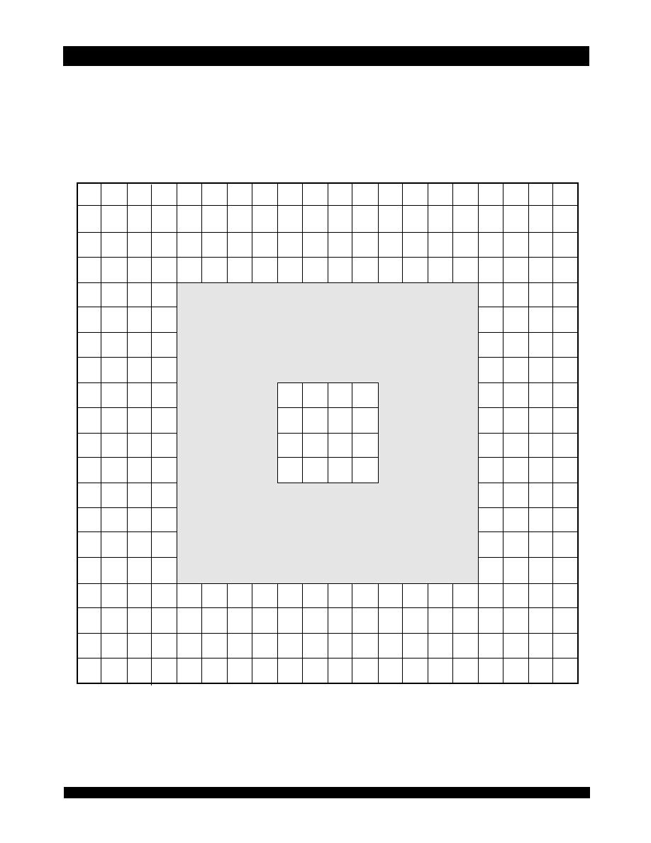
Port - 1 Logic Block Diagram
(2)
x
Counter readback on address lines
x
Mask register readback on address lines
x
Global Master reset for all ports
x
Dual Chip Enables on all ports for easy depth expansion
x
Separate upper-word and lower-word controls on all ports
x
272-BGA package (27mm x 27mm 1.27mm ball pitch) and
256-BGA package (17mm x 17mm 1.0mm ball pitch)
x
Commercial and Industrial temperature ranges
x
JTAG boundary scan
x
MBIST (Memory Built-In Self Test) controller
.eatures
x
True four-ported memory cells which allow simultaneous
access of the same memory location
x
Synchronous Pipelined device
≠ 64/32K x 18 organization
x
Pipelined output mode allows fast 200MHz operation
x
High Bandwidth up to 14 Gbps (200MHz x 18 bits wide x
4 ports)
x
LVTTL I/O interface
x
High-speed clock to data access 3.0ns (max.)
x
3.3V Low operating power
x
Interrupt flags for message passing
x
Width and depth expansion capabilities
3.3V 64/32K X 18
SYNCHRONOUS
FOURPORTTM STATIC RAM
PRELIMINARY
IDT70V5388/78
NOTE:
1.
A
15
x is a NC for IDT70V5378.
2.
Port 2, Port 3, and Port 4 Logic Blocks are similar to Port 1 Logic Blocks.
TMS
TCK
TDI
CLKMBIST
TDO
JTAG
Controller
MBIST
TRST
64KX18
Memory
Array
Port 1
Address
Decode
,
Port 1
Interrupt
Logic
INT
P1
Priority
Decision
Logic
Port 1
Counter/
Address
Register
Port 1
Mask
Register
Port 1
Readback
Register
Addr.
Read
Back
R/
W
P1
CE
0P1
CE
1P1
CLK
P1
MRST
Port 1
I/O
Control
R/
W
P1
UB
P1
CE
0P1
CE
1P1
LB
P1
OE
P1
I/O
9P1
- I/O
17P1
I/O
0P1
- I/O
8P1
CLK
P
1
MRST
CNTINT
P1
0
1
1/0
MRST
A
0P1
- A
15P1
(1)
CNTRD
P1
MKRD
P1
MKLD
P1
CNTINC
P1
CNTLD
P1
CNTRST
P1
5 64 9 d rw 0 1
x
Counter wrap-around control
≠ Internal mask register controls counter wrap-around
≠ Counter-Interrupt flags to indicate wrap-around

2
IDT70V5388/78
3.3V 64/32K x 18 Synchronous FourPortTM Static RAM Industrial and Commercial Temperature Ranges
Preliminary
Description
The IDT70V5388/78 is a high-speed 64/32Kx18 bit
synchronous FourPort RAM. The memory array utilizes
FourPort memory cells to allow simultaneous access of
any address from all four ports. Registers on control, data,
and address inputs provide minimal setup and hold times.
The timing latitude provided by this approach allows sys-
tems to be designed with very short cycle times.
With an input data register and integrated burst
counters, the 70V5388/78 has been optimized for applica-
tions having unidirectional or bi-directional data flow in
bursts. An automatic power down feature, controlled by
CE
0
and CE
1
, permits the on-chip circuitry of each port to enter
a very low standby power mode.
The IDT70V5388/78 provides a wide range of func-
tions specially designed to facilitate system operations.
These include full-boundary, maskable address counters
with associated interrupts for each port, mailbox interrupt
flags on each port to facilitate inter-port communications,
Memory Built-In Self-Test (MBIST), JTAG support and an
asynchronous Master Reset to simplify device initializa-
tion. In addition, the address lines have been set up as I/O
pins, to permit the support of
CNTRD
(the ability to output the
current value of the internal address counter on the address
lines) and
MKRD
(the ability to output the current value of the
counter mask register). For specific details on the device
operation, please refer to the Functional Description and
subsequent explanatory sections, beginning on page 21.

6.42
IDT70V5388/78
3.3V 64/32K x 18 Synchronous FourPortTM Static RAM Industrial and Commercial Temperature Ranges
5
Preliminary
Pin Definitions
P ort 1
P ort 2
P ort 3
P ort 4
Description
A
0P 1
- A
1 5P 1
(1 )
A
0P 2
- A
1 5P 2
(1 )
A
0P 3
- A
1 5P 3
(1 )
A
0P 4
- A
1 5P 4
(1 )
A d d r e s s Inp uts . In the
CNTRD
and
MKRD o p e ratio ns, the se p ins se rve
as o utp uts fo r the inte rnal ad d r e s s c o unte r and the inte rnal c o unte r m as k
re g is te r re s p e c tiv e ly.
I/O
0P 1
- I/O
1 7P 1
I/O
0P 2
- I/O
1 7P 2
I/O
0P 3
- I/0
1 7P 3
I/O
0P 4
- I/O
1 7P 4
Data B us Inp ut/Outp ut.
CLK
P 1
CLK
P 2
CLK
P 3
CLK
P 4
Clo c k Inp ut. The m axim um c lo c k inp ut rate is f
M A X
. The c lo c k s ig nal c an
b e fre e running o r s tro b e d d e p e nd ing o n s y s te m re q uire m e nts .
MRST
M as te r Re s e t Inp ut.
MRST is an asycnchro no us inp ut, and affe cts all
p o rts . It m us t b e as s e rte d LOW (
MRST = V
IL
) at initial p o we r-up . M as te r
Re s e t s e ts the inte rnal v alue o f all ad d re s s c o unte rs to z e ro , and s e ts
the c o unte r m as k re g is te rs fo r e ac h p o rt to 'unm as k e d '. It als o re s e ts the
o utp ut flag s fo r the m ailb o x e s and the c o unte r inte rrup ts (
INT = CNTINT =
V
IH
) and d e s e le c ts all re g is te re d c o ntro l s ig nals .
CE
0P 1
, CE
1P 1
CE
0P 2
, CE
1P 2
CE
0P 3
, CE
1P 3
CE
0P 4
, CE
1P 4
Chip E nab le Inp uts . To activ ate any p o rt, b o th s ig nals m us t b e as s e rte d
to the ir ac tiv e s tate s
(
CE
0
= V
IL
, CE
1
= V
IH
).
A
g iv e n p o rt is d is ab le d if
e ithe r c hip e nab le is d e as se rte d
(
CE
0
= V
IH
and /o r CE
1
= V
IL
).
R/
W
P I
R/
W
P 2
R/
W
P 3
R/
W
P 4
Re ad /Write Enab le Inp ut. Th is sig nal is as s e rte d LOW (R/
W = V
IL
)
in
o rd e r to write to the Fo urP o rt m e m o ry array, a nd it is as s e rte d
HIGH
(R/
W = V
IH
)
in o rd e r to re ad fro m the array.
LB
P 1
LB
P 2
LB
P 3
LB
P 4
Lo we r B y te S e le c t Inp ut (I/O
0
- I/O
8
).
A s s e rting this s ig nal LOW (
LB = V
IL
)
e nab le s re ad /write
o p e ratio ns to the lo we r b y te .
Fo r re ad o p e ratio ns , this
s ig nal is us e d in c o njunc tio n with
OE
in o rd e r to d riv e o utp ut d ata o n the
lo we r b y te o f the d ata b us .
UB
P 1
UB
P 2
UB
P 3
UB
P 4
Up p e r B y te Se le c t Inp ut (I/O
9
- I/O
1 7
).
A s s e rting this s ig nal LOW (
LB =
V
IL
)
e nab le s re ad /write
o p e ratio ns to the up p e r b y te .
Fo r re ad
o p e ratio ns , this s ig nal is us e d in c o njunc tio n with
OE
in o rd e r to d riv e
o utp ut d ata o n the up p e r b y te o f the d ata b us .
OE
P 1
OE
P 2
OE
P 3
OE
P 4
Outp ut Enab le Inp u t. As s e rting this s ig nal LOW (
OE = V
IL
) e nab le s the
d e v ic e to d riv e d ata o n th I/O p ins d uring re ad o p e ratio n.
OE is an
as y c hro no us inp ut.
CNTLD
P 1
CNTLD
P 2
CNTLD
P 3
CNTLD
P 4
Co unte r Lo ad Inp u t. As s e rting this s ig nal LOW (
CNTLD = V
IL
) lo ad s the
ad d re s s o n the ad d re s s line s (A
0
- A
1 5
(1 )
) into the inte rnal ad d re s s
c o unte r fo r that p o rt.
CNTINC
P 1
CNTINC
P 2
CNTINC
P 3
CNTINC
P 4
Co unte r In c re m e nt Inp u t. As s e rting this s ig nal LOW (
CNTINC = V
IL
)
inc re m e nts the inte rnal ad d re s s c o unte r fo r that p o rt o n e ac h ris ing e d g e
o f the c lo c k s ig nal. The c o unte r will inc re m e nt as d e fine d b y the c o unte r
m as k re g is te r fo r that p o rt (d e fault m o d e i s to ad v anc e o ne ad d re s s o n
e ac h c lo c k c y c le ).
CNTRD
P 1
CNTRD
P 2
CNTRD
P 3
CNTRD
P 4
Co unte r Re ad b ac k Inp ut. Whe n as s e rte d LOW (
CNTRD = V
IL
) c aus e s that
p o rt to o utp ut the v alue o f its inte rnal ad d re s s c o unte r o n the ad d re s s
line s fo r that p o rt. Co unte r re a d b ac k is ind e p e nd e nt o f the c hip e nab le s
fo r that p o rt.
If the p o rt is ac tiv ate d
(
CE
0
= V
IL
and CE
1
= V
IH
),
d uring the
c o unte r re ad b ac k o p e ratio n, the n the d ata b us will o utp ut the d ata
as s o c iate d with that re ad b a c k ad d re s s in the Fo urP o rt m e m o ry array
(as s um ing that the b y te e nab l e s and o utp ut e nab le s are als o as s e rte d ).
Truth Tab le III ind ic ate s the re q uire d s tate s fo r all o the r c o unte r c o ntro ls
d uring this o p e ratio n. The s p e c ific o p e ratio n and tim ing o f this func io n is
d e s c rib e d in d e tail in the te x t.
CNTRST
P 1
CNTRST
P 2
CNTRST
P 3
CNTRST
P 4
Co un te r Re s e t Inp ut. A s s e rting this s ig nal LOW
(
CNTRST = V
IL
)
re s e ts
the ad d re s s c o unte r fo r that p o rt to z e ro .
CNTINT
P 1
CNTINT
P 2
CNTINT
P 3
CNTINT
P 4
Co unte r Inte rrup t F lag Outp ut
.
This s ig nal is as s e rte d LOW (
CNTINT =
V
IL
) whe n the inte rnal ad d re s s c o unte r fo r that p o rt 'wrap s aro und ' fro m
m ax ad d re s s [(the c o unte r will i nc re m e nt as d e fine d b y the c o unte r m as k
re g is te r fo r that p o rt (d e fault m o d e is to ad v anc e o ne ad d re s s o n e ac h
c lo c k c y c le )] to ad d re s s m in. as th e re s ult o f c o unte r inc re m e nt (
CNTINT
= V
IL
). The s ig nal g o e s LO W fo r o ne c lo c k c y c le , the n auto m atic ally
re s e ts .
5 6 49 tb l 0 1