 | –≠–ª–µ–∫—Ç—Ä–æ–Ω–Ω—ã–π –∫–æ–º–ø–æ–Ω–µ–Ω—Ç: 70V639 | –°–∫–∞—á–∞—Ç—å:  PDF PDF  ZIP ZIP |
©2001 Integrated Device Technology, Inc.
JUNE 2001
DSC-5621/3
1
CE
0R
R/
W
R
CE
1R
LB
R
UB
R
128K x 18
MEMORY
ARRAY
Address
Decoder
A
16 R
A
0R
Address
Decoder
CE
0 L
R/
W
L
CE
1 L
LB
L
UB
L
Dout0-8_L
Dout9-17_L
Dout0-8_R
Dout9-17_R
B
E
0
L
B
E
1
L
B
E
1
R
B
E
0
R
I/O
0L
- I/O
17L
I/O
0R
- I/O
17R
Din_L
ADDR_L
Din_R
ADDR_R
OE
R
OE
L
ARBITRATION
INT ERRUPT
SEMAPHORE
LOGIC
SEM
L
INT
L
BUSY
L
M/
S
R/
W
L
OE
L
R/
W
R
OE
R
BUSY
R
SEM
R
INT
R
CE
0L
CE
1L
CE
0 R
CE
1 R
TMS
TCK
TRST
TDI
TDO
JTAG
5 621 drw 01
A
16L
A
0L
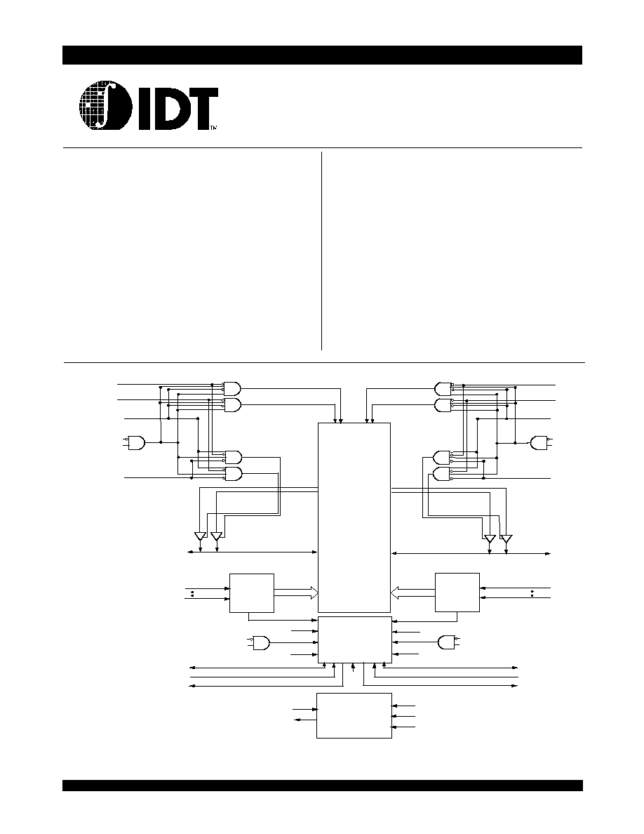
Functional Block Diagram
x
x
x
x
x
Fully asynchronous operation from either port
x
Separate byte controls for multiplexed bus and bus
matching compatibility
x
x
x
x
x
Supports JTAG features compliant to IEEE 1149.1
≠ Due to limited pin count, JTAG is not supported on the
128-pin TQFP package.
x
x
x
x
x
LVTTL-compatible, single 3.3V (±150mV) power supply for
core
x
x
x
x
x
LVTTL-compatible, selectable 3.3V (±150mV)/2.5V (±100mV)
power supply for I/Os and control signals on each port
x
x
x
x
x
Available in a 128-pin Thin Quad Flatpack, 208-ball fine
pitch Ball Grid Array, and 256-ball Ball Grid Array
x
x
x
x
x
Industrial temperature range (≠40∞C to +85∞C) is available
for selected speeds
Features
x
x
x
x
x
True Dual-Port memory cells which allow simultaneous
access of the same memory location
x
x
x
x
x
High-speed access
≠ Commercial: 10/12/15ns (max.)
≠ Industrial: 12/15ns (max.)
x
x
x
x
x
Dual chip enables allow for depth expansion without
external logic
x
x
x
x
x
IDT70V639 easily expands data bus width to 36 bits or
more using the Master/Slave select when cascading more
than one device
x
x
x
x
x
M/
S = V
IH
for
BUSY output flag on Master,
M/
S = V
IL
for
BUSY input on Slave
x
x
x
x
x
Busy and Interrupt Flags
x
x
x
x
x
On-chip port arbitration logic
x
x
x
x
x
Full on-chip hardware support of semaphore signaling
between ports
HIGH-SPEED 3.3V 128K x 18
ASYNCHRONOUS DUAL-PORT
STATIC RAM
PRELIMINARY
IDT70V639S
NOTES:
1.
BUSY is an input as a Slave (M/S=V
IL
) and an output when it is a Master (M/
S=V
IH
).
2.
BUSY and INT are non-tri-state totem-pole outputs (push-pull).

IDT70V639S Preliminary
High-Speed 3.3V 128K x 18 Asynchronous Dual-Port Static RAM Industrial and Commercial Temperature Ranges
2
Description
The IDT70V639 is a high-speed 128K x 18 Asynchronous Dual-Port
Static RAM. The IDT70V639 is designed to be used as a stand-alone
2304K-bit Dual-Port RAM or as a combination MASTER/SLAVE Dual-
Port RAM for 36-bit-or-more word system. Using the IDT MASTER/
SLAVE Dual-Port RAM approach in 36-bit or wider memory system
applications results in full-speed, error-free operation without the need for
additional discrete logic.
This device provides two independent ports with separate control,
address, and I/O pins that permit independent, asynchronous access for
reads or writes to any location in memory. An automatic power down
feature controlled by the chip enables (either
CE
0
or CE
1
) permit the
on-chip circuitry of each port to enter a very low standby power mode.
The 70V639 can support an operating voltage of either 3.3V or 2.5V
on one or both ports, controlled by the OPT pins. The power supply for
the core of the device (V
DD
) remains at 3.3V.
Pin Configurations
(1,2,3,4)
NOTES:
1. All V
DD
pins must be connected to 3.3V power supply.
2. All V
DDQ
pins must be connected to appropriate power supply: 3.3V if OPT pin for that port is set to V
IH
(3.3V) and 2.5V if OPT pin for that port is
set to V
IL
(0V).
3. All V
SS
pins must be connected to ground.
4. Package body is approximately 15mm x 15mm x 1.4mm with 0.8mm ball pitch.
5. This package code is used to reference the package diagram.
6. This text does not indicate orientation of the actual part-marking.
17
16
15
14
12
13
10
9
8
7
6
5
4
3
2
1
11
A
B
C
D
E
F
G
H
J
K
L
M
N
P
R
T
U
I/O
9L
NC
V
SS
A
4L
INT
L
SEM
L
NC
A
8L
A
12L
A
16L
V
SS
NC
OPT
L
A
0L
NC
V
SS
NC
NC
A
1L
A
5L
BUSY
L
V
SS
CE
0L
CE
1L
NC
A
9L
A
13L
NC
I/O
8L
V
DDQR
V
SS
V
DDQL
I/O
9R
V
DDQR
V
DD
A
2L
A
6
L
R /
W
L
V
SS
UB
L
A
10L
A
14L
NC
NC
I/O
8R
V
DD
I/O
11L
V
SS
I/O
10L
NC
V
DD
A
3L
NC
OE
L
NC
I/O
11R
V
DDQR
I/O
10R
V
DDQL
NC
NC
V
SS
NC
V
SS
I/O
12L
NC
V
DD
NC
V
DDQR
I/O
12R
V
DDQL
V
DD
V
SS
V
SS
NC
I/O
14L
V
DDQR
V
DDQL
NC
I/O
15R
V
SS
I/O
7R
V
DDQL
I/O
7L
A
15L
A
11 L
A
7L
LB
L
I/O
6L
NC
V
SS
NC
V
SS
I/O
6R
NC
NC
V
DDQL
I/O
5L
NC
V
DD
NC
V
SS
I/O
5R
V
SS
V
DDQR
I/O
3R
V
DDQL
I/O
4R
V
SS
I/O
4L
V
SS
I/O
3L
NC
A
0R
A
1R
A
2R
A
3R
A
4R
A
5R
A
6R
I/O
1R
NC
V
SS
NC
I/O
15L
A
16R
A
12R
A
8R
NC
V
DD
SEM
R
INT
R
V
DDQR
NC
I/O
1L
NC
V
SS
NC
I/O
17R
NC
A
13R
A
9R
NC
CE
0R
CE
1R
V
DD
V
SS
BUSY
R
V
SS
V
DD
V
SS
V
DDQL
I/O
0R
V
DDQR
NC
I/O
17L
V
DDQL
NC
NC
A
14R
A
10R
UB
R
V
SS
NC
NC
V
SS
I/O
2R
NC
V
SS
NC
V
DD
A
15R
A
11R
A
7R
LB
R
OE
R
M/
S
R/
W
R
V
DDQL
I/O
2L
OPT
R
NC
I/O
0 L
70V639BF
BF-208
(5)
208-Ball BGA
Top View
(6)
5621 tbl 02b
I/O
13L
I/O
14R
V
SS
I/O
13R
V
SS
I/O
16R
I/O
16L
V
DDQR
NC
A
B
C
D
E
F
G
H
J
K
L
M
N
P
R
T
U
V
SS
NC
NC
V
DDQR
V
SS
V
DD
V
SS
NC
V
DD
V
DD
TDO
TDI
TCK
TMS
TRST
V
SS
IDT70V639S Preliminary
High-Speed 3.3V 128K x 18 Asynchronous Dual-Port Static RAM Industrial and Commercial Temperature Ranges
3
NOTES:
1. All V
DD
pins must be connected to 3.3V power supply.
2. All V
DDQ
pins must be connected to appropriate power supply: 3.3V if OPT pin for that port is set to V
IH
(3.3V) and 2.5V if OPT pin for that port is
set to V
IL
(0V).
3. All V
SS
pins must be connected to ground.
4. Package body is approximately 14mm x 20mm x 1.4mm.
5. This package code is used to reference the package diagram.
6. This text does not indicate orientation of the actual part-marking.
7. Due to the restricted number of pins, JTAG is not supported in the PK-128 package.
1
2
3
4
5
6
7
8
9
10
11
12
13
14
15
16
17
18
19
20
21
22
23
24
25
26
27
28
29
30
31
32
33
34
35
36
37
38
102
101
100
99
98
97
96
95
94
93
92
90
89
88
87
86
85
84
83
82
81
80
79
78
77
76
75
74
73
72
70
69
68
67
66
65
91
71
A
14L
A
15L
A
16L
NC
IO
9L
IO
9R
V
DDQL
V
SS
IO
10L
IO
10R
V
DDQR
V
SS
IO
11L
IO
11R
IO
12L
IO
12R
V
DD
V
DD
V
SS
V
SS
IO
13R
IO
13L
IO
14R
IO
14L
IO
15R
IO
15L
V
DDQL
V
SS
IO
16R
IO
16L
V
DDQR
V
SS
IO
17R
IO
17L
NC
A
16R
A
15R
A
14R
A
1R
A
0R
OPT
R
IO
0L
IO
0R
V
DDQR
V
SS
IO
1L
IO
1R
V
DDQL
V
SS
IO
2L
IO
2R
IO
3L
IO
3R
IO
4L
IO
4R
V
SS
V
SS
V
DD
V
DD
IO
5L
IO
5R
V
DDQR
V
SS
IO
7R
IO
7L
V
DDQL
V
SS
NC
IO
8R
IO
8L
V
SS
OPT
L
A
0L
A
1L
IO
6R
IO
6L
70V639PRF
PK-128
(5)
128-Pin TQFP
Top View
(6)
5621 drw 02a
A
1
3
L
A
1
2
L
A
1
1
L
A
1
0
L
A
9
L
A
8
L
A
7
L
U
B
L
L
B
L
C
E
1
L
C
E
0
L
V
D
D
V
D
D
V
S
S
V
S
S
S
E
M
L
O
E
L
R
/
W
L
B
U
S
Y
L
I
N
T
L
N
C
A
6
L
A
5
L
A
4
L
A
3
L
A
2
L
A
1
3
R
A
1
2
R
A
1
1
R
A
1
0
R
A
9
R
A
8
R
A
7
R
U
B
R
L
B
R
C
E
1
R
C
E
0
R
V
D
D
V
D
D
V
S
S
V
S
S
S
E
M
R
O
E
R
R
/
W
R
B
U
S
Y
R
I
N
T
R
M
/
S
A
6
R
A
5
R
A
4
R
A
3
R
A
2
R
3
9
4
0
4
1
4
2
4
3
4
4
4
5
4
6
4
7
4
8
4
9
5
0
5
1
5
2
5
3
5
4
5
5
5
6
5
7
5
8
5
9
6
0
6
1
6
2
6
3
6
4
1
2
8
1
2
7
1
2
6
1
2
5
1
2
4
1
2
3
1
2
2
1
2
1
1
2
0
1
1
9
1
1
8
1
1
7
1
1
6
1
1
5
1
1
4
1
1
3
1
1
2
1
1
1
1
1
0
1
0
9
1
0
8
1
0
7
1
0
6
1
0
5
1
0
4
1
0
3
.
Pin Configurations
(1,2,3,4,7)
(con't.)

IDT70V639S Preliminary
High-Speed 3.3V 128K x 18 Asynchronous Dual-Port Static RAM Industrial and Commercial Temperature Ranges
4
Pin Configuration
(1,2,3,4)
(con't.)
NOTES:
1. All V
DD
pins must be connected to 3.3V power supply.
2. All V
DDQ
pins must be connected to appropriate power supply: 3.3V if OPT pin for that port is set to V
IH
(3.3V), and 2.5V if OPT pin for that port is
set to V
IL
(0V).
3. All V
SS
pins must be connected to ground supply.
4. Package body is approximately 17mm x 17mm x 1.4mm, with 1.0mm ball-pitch.
5. This package code is used to reference the package diagram.
6. This text does not indicate orientation of the actual part-marking.
70V639BC
BC-256
(5)
256-Pin BGA
Top View
(6)
E16
I/O
7R
D16
I/O
8R
C16
I/O
8L
B16
NC
A16
NC
A15
NC
B15
NC
C15
NC
D15
NC
E15
I/O
7L
E14
NC
D14
NC
D13
V
DD
C12
A
6L
C14
OPT
L
B14
NC
A14
A
0L
A12
A
5L
B12
A
4L
C11
BUSY
L
D12
V
DDQR
D11
V
DDQR
C10
SEM
L
B11
NC
A11
INT
L
D8
V
DDQR
C8
NC
A9
CE
1L
D9
V
DDQL
C9
LB
L
B9
CE
0L
D10
V
DDQL
C7
A
7L
B8
UB
L
A8
NC
B13
A
1L
A13
A
2L
A10
OE
L
D7
V
DDQR
B7
A
9L
A7
A
8L
B6
A
12L
C6
A
10L
D6
V
DDQL
A5
A
14L
B5
A
15L
C5
A
13L
D5
V
DDQL
A4
NC
B4
NC
C4
A
16L
D4
V
DD
A3
NC
B3
TDO
C3
V
SS
D3
NC
D2
I/O
9R
C2
I/O
9L
B2
NC
A2
TDI
A1
NC
B1
NC
C1
NC
D1
NC
E1
I/O
10R
E2
I/O
10L
E3
NC
E4
V
DDQL
F1
I/O
11L
F2
NC
F3
I/O
11R
F4
V
DDQL
G1
NC
G2
NC
G3
I/O
12L
G4
V
DDQR
H1
NC
H2
I/O
12R
H3
NC
H4
V
DDQR
J1
I/O
13L
J2
I/O
14R
J3
I/O
13R
J4
V
DDQL
K1
NC
K2
NC
K3
I/O
14L
K4
V
DDQL
L1
I/O
15L
L2
NC
L3
I/O
15R
L4
V
DDQR
M1
I/O
16R
M2
I/O
16L
M3
NC
M4
V
DDQR
N1
NC
N2
I/O
17R
N3
NC
N4
V
DD
P1
NC
P2
I/O
17L
P3
TMS
P4
A
16R
R1
NC
R2
NC
R3
TRST
R4
NC
T1
NC
T2
TCK
T3
NC
T4
NC
P5
A
13R
R5
A
15R
P12
A
6R
P8
NC
P9
LB
R
R8
UB
R
T8
NC
P10
SEM
R
T11
INT
R
P11
BUSY
R
R12
A
4R
T12
A
5R
P13
A
3R
P7
A
7R
R13
A
1R
T13
A
2R
R6
A
12R
T5
A
14R
T14
A
0R
R14
OPT
R
P14
NC
P15
NC
R15
NC
T15
NC
T16
NC
R16
NC
P16
I/O
0L
N16
NC
N15
I/O
0R
N14
NC
M16
NC
M15
I/O
1L
M14
I/O
1R
L16
I/O
2R
L15
NC
L14
I/O
2L
K16
I/O
3L
K15
NC
K14
NC
J16
I/O
4L
J15
I/O
3R
J14
I/O
4R
H16
I/O
5R
H15
NC
H14
NC
G16
NC
G15
NC
G14
I/O
5L
F16
I/O
6L
F14
I/O
6R
F15
NC
R9
CE
0R
R11
M/
S
T6
A
11R
T9
CE
1R
A6
A
11L
B10
R/
W
L
C13
A
3L
P6
A
10R
R10
R/
W
R
R7
A
9R
T10
OE
R
T7
A
8R
,
E5
V
DD
E6
V
DD
E7
V
SS
E8
V
SS
E9
V
SS
E10
V
SS
E11
V
DD
E12
V
DD
E13
V
DDQR
F5
V
DD
F6
V
SS
F8
V
SS
F9
V
SS
F10
V
SS
F12
V
DD
F13
V
DDQR
G5
V
SS
G6
V
SS
G7
V
SS
G8
V
SS
G9
V
SS
G10
V
SS
G11
V
SS
G12
V
SS
G13
V
DDQL
H5
V
SS
H6
V
SS
H7
V
SS
H8
V
SS
H9
V
SS
H10
V
SS
H11
V
SS
H12
V
SS
H13
V
DDQL
J5
V
SS
J6
V
SS
J7
V
SS
J8
V
SS
J9
V
SS
J10
V
SS
J11
V
SS
J12
V
SS
J13
V
DDQR
K5
V
SS
K6
V
SS
K7
V
SS
K8
V
SS
L5
V
DD
L6
V
SS
L7
V
SS
L8
V
SS
M5
V
DD
M6
V
DD
M7
V
SS
M8
V
SS
N5
V
DDQR
N6
V
DDQR
N7
V
DDQL
N8
V
DDQL
K9
V
SS
K10
V
SS
K11
V
SS
K12
V
SS
L9
V
SS
L10
V
SS
L11
V
SS
L12
V
DD
M9
V
SS
M10
V
SS
M11
V
DD
M12
V
DD
N9
V
DDQR
N10
V
DDQR
N11
V
DDQL
N12
V
DDQL
K13
V
DDQR
L13
V
DDQL
M13
V
DDQL
N13
V
DD
F7
V
SS
F11
V
SS
5621 drw 02c
,

IDT70V639S Preliminary
High-Speed 3.3V 128K x 18 Asynchronous Dual-Port Static RAM Industrial and Commercial Temperature Ranges
5
Pin Names
NOTES:
1. V
DD
, OPT
X
, and V
DDQX
must be set to appropriate operating levels prior to
applying inputs on I/O
X
.
2. OPT
X
selects the operating voltage levels for the I/Os and controls on that port.
If OPT
X
is set to V
IH
(3.3V), then that port's I/Os and controls will operate at 3.3V
levels and V
DDQX
must be supplied at 3.3V. If OPT
X
is set to V
IL
(0V), then that
port's I/Os and controls will operate at 2.5V levels and V
DDQX
must be supplied
at 2.5V. The OPT pins are independent of one another--both ports can operate
at 3.3V levels, both can operate at 2.5V levels, or either can operate at 3.3V
with the other at 2.5V.
Left Port
Right Port
Names
CE
0L
,
CE
1L
CE
0R
,
CE
1R
Chip Enables
R/
W
L
R/
W
R
Read/Write Enable
OE
L
OE
R
Output Enable
A
0L
- A
16L
A
0R
- A
16R
Address
I/O
0L
- I/O
17L
I/O
0R
- I/O
17R
Data Input/Output
SEM
L
SEM
R
Semaphore Enable
INT
L
INT
R
Interrupt Flag
BUSY
L
BUSY
R
Busy Flag
UB
L
UB
R
Upper Byte Select
LB
L
LB
R
Lower Byte Select
V
DDQL
V
DDQR
Power (I/O Bus) (3.3V or 2.5V)
(1)
OPT
L
OPT
R
Option for selecting V
DDQX
(1,2)
M/
S
Master or Slave Select
V
DD
Power (3.3V)
(1)
V
SS
Ground (0V)
TDI
Test Data Input
TDO
Test Data Output
TCK
Test Logic Clock (10MHz)
TMS
Test Mode Select
TRST
Reset (Initialize TAP Controller)
5621 tbl 01