 | –≠–ª–µ–∫—Ç—Ä–æ–Ω–Ω—ã–π –∫–æ–º–ø–æ–Ω–µ–Ω—Ç: 70V7519 | –°–∫–∞—á–∞—Ç—å:  PDF PDF  ZIP ZIP |

©2002 Integrated Device Technology, Inc.
DECEMBER 2002
DSC 5618/5
1
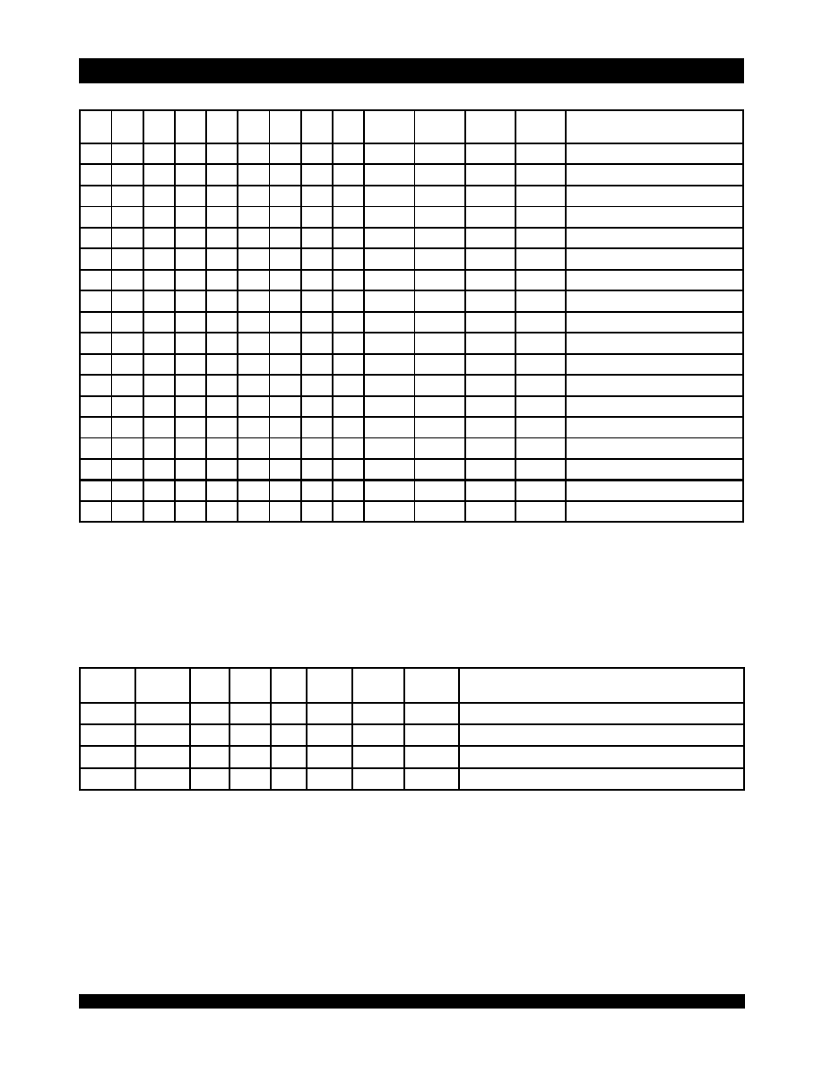
Functional Block Diagram
Features:
x
256K x 36 Synchronous Bank-Switchable Dual-ported
SRAM Architecture
≠ 64 independent 4K x 36 banks
≠ 9 megabits of memory on chip
x
Bank access controlled via bank address pins
x
High-speed data access
≠ Commercial: 3.4ns(200MHz)/3.6ns (166MHz)/4.2ns
(133MHz) (max.)
≠ Industrial: 3.6ns (166MHz)/4.2ns (133MHz) (max.)
x
Selectable Pipelined or Flow-Through output mode
x
Counter enable and repeat features
x
Dual chip enables allow for depth expansion without
additional logic
x
Full synchronous operation on both ports
≠ 5ns cycle time, 200MHz operation (14Gbps bandwidth)
≠ Fast 3.4ns clock to data out
≠ 1.5ns setup to clock and 0.5ns hold on all control, data, and
address inputs @ 200MHz
≠ Data input, address, byte enable and control registers
≠ Self-timed write allows fast cycle time
x
Separate byte controls for multiplexed bus and bus
matching compatibility
x
LVTTL- compatible, 3.3V (±150mV) power supply
for core
x
LVTTL compatible, selectable 3.3V (±150mV) or 2.5V
(±100mV) power supply for I/Os and control signals on
each port
x
Industrial temperature range (-40∞C to +85∞C) is
available at 166MHz and 133MHz
x
Available in a 208-pin Plastic Quad Flatpack (PQFP),
208-pin fine pitch Ball Grid Array (fpBGA), and 256-pin Ball
Grid Array (BGA)
x
Supports JTAG features compliant with IEEE 1149.1
HIGH-SPEED 3.3V 256K x 36
SYNCHRONOUS
BANK-SWITCHABLE
DUAL-PORT STATIC RAM
WITH 3.3V OR 2.5V INTERFACE
IDT70V7519S
4Kx36
MEMORY
ARRAY
(BANK 63)
MUX
MUX
PL/
FT
L
OPT
L
CLK
L
ADS
L
CNTEN
L
REPEAT
L
R/
W
L
CE
0L
CE
1L
BE
3L
BE
2L
BE
1L
BE
0L
OE
L
I/O
0L-35L
A
11L
A
0L
JTAG
4Kx36
MEMORY
ARRAY
(BANK 1)
MUX
MUX
4Kx36
MEMORY
ARRAY
(BANK 0)
MUX
MUX
CONTROL
LOGIC
I/O
CONTROL
BANK
DECODE
ADDRESS
DECODE
I/O
0R-35R
A
11R
A
0R
CONTROL
LOGIC
I/O
CONTROL
BANK
DECODE
ADDRESS
DECODE
5618 drw 01
BA
5R
BA
4R
BA
3R
BA
2R
BA
1R
BA
0R
BA
5L
BA
4L
BA
3L
BA
2L
BA
1L
BA
0L
,
PL/
FT
R
OPT
R
CLK
R
ADS
R
CNTEN
R
REPEAT
R
R/
W
R
CE
0R
CE
1R
BE
3R
BE
2R
BE
1R
BE
0R
OE
R
TMS
TCK
TRST
TDI
TDO
NOTE:
1. The Bank-Switchable dual-port uses a true SRAM
core instead of the traditional dual-port SRAM core.
As a result, it has unique operating characteristics.
Please refer to the functional description on page 19
for details.

6.42
2
IDT70V7519S
High-Speed 256K x 36 Synchronous Bank-Switchable Dual-Port Static RAM Industrial and Commercial Temperature Ranges
Description:
The IDT70V7519 is a high-speed 256Kx36 (9Mbit) synchronous
Bank-Switchable Dual-Ported SRAM organized into 64 independent
4Kx36 banks. The device has two independent ports with separate
control, address, and I/O pins for each port, allowing each port to access
any 4Kx36 memory block not already accessed by the other port.
Accesses by the ports into specific banks are controlled via the bank
address pins under the user's direct control.
Registers on control, data, and address inputs provide minimal setup
and hold times. The timing latitude provided by this approach allows
systems to be designed with very short cycle times. With an input data
Pin Configuration
(1,2,3,4)
NOTES:
1. All V
DD
pins must be connected to 3.3V power supply.
2. All V
DDQ
pins must be connected to appropriate power supply: 3.3V if OPT pin for that port is set to V
IH
(3.3V), and 2.5V if OPT pin for that port is
set to V
IL
(0V).
3. All V
SS
pins must be connected to ground supply.
4. Package body is approximately 15mm x 15mm x 1.4mm with 0.8mm ball pitch.
5. This package code is used to reference the package diagram.
6. This text does not indicate orientation of the actual part-marking.
A17
V
SS
B17
I/O
15R
C17
V
SS
D17
I/O
14R
E16
V
SS
E17
I/O
13L
D16
I/O
14L
C16
I/O
15L
B16
I/O
16L
A16
I/O
17L
A15
OPT
L
B15
V
DDQR
C15
I/O
16R
D15
V
DDQL
E15
I/O
13R
E14
I/O
12L
D14
I/O
17R
D13
V
DD
C12
A
6L
C14
V
DD
B14
V
SS
A14
A
0L
A12
CNTEN
L
B12
A
5L
C11
R/
W
L
D12
A
3L
D11
REPEAT
L
C10
V
SS
B11
ADS
L
A11
CLK
L
D8
BE
0L
C8
BE
3L
A9
BE
1L
D9
V
DD
C9
CE
1L
B9
CE
0L
D10
OE
L
C7
A
10L
B8
BE
2L
A8
A
8L
B13
A
1L
A13
A
4L
A10
V
DD
D7
A
7L
B7
A
9L
A7
BA
0L
B6
BA
1L
C6
BA
2L
D6
A
11L
A5
NC
B5
BA
5L
C5
NC
D5
BA
3L
A4
TDO
B4
TDI
C4
PL/
FT
L
D4
I/O
20L
A3
V
SS
B3
I/O
18R
C3
V
DDQR
D3
I/O
21L
D2
V
SS
C2
I/O
19R
B2
V
SS
A2
IO
18L
A1
IO
19L
B1
I/O
20R
C1
V
DDQL
D1
I/O
22L
E1
I/O
23L
E2
I/O
22R
E3
V
DDQR
E4
I/O
21R
F1
V
DDQL
F2
I/O
23R
F3
I/O
24L
F4
V
SS
G1
I/O
26L
G2
V
SS
G3
I/O
25L
G4
I/O
24R
H1
V
DD
H2
I/O
26R
H3
V
DDQR
H4
I/O
25R
J1
V
DDQL
J2
V
DD
J3
V
SS
J4
V
SS
K1
I/O
28R
K2
V
SS
K3
I/O
27R
K4
V
SS
L1
I/O
29R
L2
I/O
28L
L3
V
DDQR
L4
I/O
27L
M1
V
DDQL
M2
I/O
29L
M3
I/O
30R
M4
V
SS
N1
I/O
31L
N2
V
SS
N3
I/O
31R
N4
I/O
30L
P1
I/O
32R
P2
I/O
32L
P3
V
DDQR
P4
I/O
35R
R1
V
SS
R2
I/O
33L
R3
I/O
34R
R4
TCK
T1
I/O
33R
T2
I/O
34L
T3
V
DDQL
T4
TMS
U1
V
SS
U2
I/O
35L
U3
PL/
FT
R
U4
NC
P5
TRST
R5
BA
5R
U6
A
11R
P12
CNTEN
R
P8
A
8R
U10
OE
R
P9
BE
1R
R8
BE
2R
T8
BE
3R
U9
V
DD
P10
V
DD
T11
R/
W
R
U8
BE
0R
P11
CLK
R
R12
A
5R
T12
A
6R
U12
A
3R
P13
A
4R
P7
BA
0R
R13
A
1R
T13
A
2R
U13
A
0R
R6
BA
1R
T5
NC
U7
A
7R
U14
V
DD
T14
V
SS
R14
V
SS
P14
I/O
2L
P15
I/O
3L
R15
V
DDQL
T15
I/O
0R
U15
OPT
R
U16
I/O
0L
U17
I/O
1L
T16
V
SS
T17
I/O
2R
R17
V
DDQR
R16
I/O
1R
P17
I/O
4L
P16
V
SS
N17
I/O
5L
N16
I/O
4R
N15
V
DDQL
N14
I/O
3R
M17
V
DDQR
M16
I/O
5R
M15
I/O
6L
M14
V
SS
L17
I/O
8L
L16
V
SS
L15
I/O
7L
L14
I/O
6R
K17
V
SS
K16
I/O
8R
K15
V
DDQL
K14
I/O
7R
J17
V
DDQR
J16
V
SS
J15
V
DD
J14
V
SS
H17
I/O
10R
H16
V
SS
H15
IO
9R
H14
V
DD
G17
I/O
11R
G16
I/O
10L
G15
V
DDQL
G14
I/O
9L
F17
V
DDQR
F16
I/O
11L
F14
V
SS
70V7519BF
BF-208
(5)
208-Pin fpBGA
Top View
(6)
F15
I/O
12R
R9
CE
0R
R11
ADS
R
T6
BA
2R
T9
CE
1R
A6
BA
4L
B10
V
SS
C13
A
2L
P6
BA
4R
R10
V
SS
R7
A
9R
T10
V
SS
T7
A
10R
U5
BA
3R
5618 drw 02c
,
01/11/02
register, the IDT70V7519 has been optimized for applications having
unidirectional or bidirectional data flow in bursts. An automatic power down
feature, controlled by CE
0
and CE
1
, permits the on-chip circuitry of each
port to enter a very low standby power mode. The dual chip enables also
facilitate depth expansion.
The 70V7519 can support an operating voltage of either 3.3V or 2.5V
on one or both ports, controllable by the OPT pins. The power supply for
the core of the device(V
DD
) remains at 3.3V. Please refer also to the
functional description on page 19.

6.42
IDT70V7519S
High-Speed 256K x 36 Synchronous Bank-Switchable Dual-Port Static RAM Industrial and Commercial Temperature Ranges
3
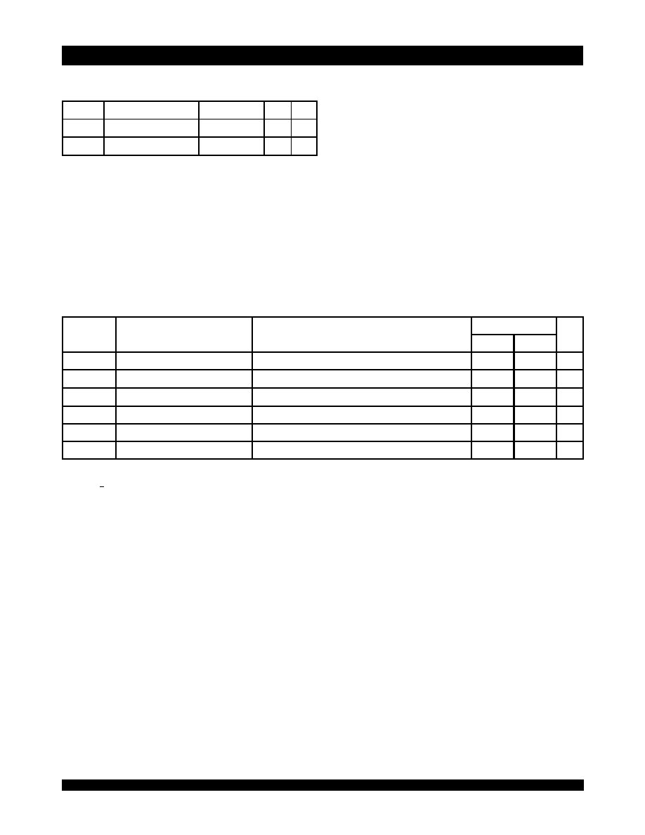
Pin Configuration
(1,2,3,4)
(con't.)
NOTES:
1. All V
DD
pins must be connected to 3.3V power supply.
2. All V
DDQ
pins must be connected to appropriate power supply: 3.3V if OPT pin for that port is set to V
IH
(3.3V), and 2.5V if OPT pin for that port is
set to V
IL
(0V).
3. All V
SS
pins must be connected to ground supply.
4. Package body is approximately 17mm x 17mm x 1.4mm, with 1.0mm ball-pitch.
5. This package code is used to reference the package diagram.
6. This text does not indicate orientation of the actual part-marking.
70V7519BC
BC-256
(5)
256-Pin BGA
Top View
(6)
E16
I/O
14R
D16
I/O
16R
C16
I/O
16L
B16
NC
A16
NC
A15
NC
B15
I/O
17L
C15
I/O
17R
D15
I/O
15L
E15
I/O
14L
E14
I/O
13L
D14
I/O
15R
D13
V
DD
C12
A
6L
C14
OPT
L
B14
V
DD
A14
A
0L
A12
A
5L
B12
A
4L
C11
ADS
L
D12
V
DDQR
D11
V
DDQR
C10
CLK
L
B11
REPEAT
L
A11
CNTEN
L
D8
V
DDQR
C8
BE
1L
A9
CE
1L
D9
V
DDQL
C9
BE
0L
B9
CE
0L
D10
V
DDQL
C7
A
7L
B8
BE
3L
A8
BE
2L
B13
A
1L
A13
A
2L
A10
OE
L
D7
V
DDQR
B7
A
9L
A7
A
8L
B6
BA
0L
C6
A
10L
D6
V
DDQL
A5
BA
2L
B5
BA
3L
C5
BA
1L
D5
V
DDQL
A4
BA
5L
B4
NC
C4
BA
4L
D4
PL/
FT
L
A3
NC
B3
TDO
C3
V
SS
D3
I/O
20L
D2
I/O
19R
C2
I/O
19L
B2
NC
A2
TDI
A1
NC
B1
I/O
18L
C1
I/O
18R
D1
I/O
20R
E1
I/O
21R
E2
I/O
21L
E3
I/O
22L
E4
V
DDQL
F1
I/O
23L
F2
I/O
22R
F3
I/O
23R
F4
V
DDQL
G1
I/O
24R
G2
I/O
24L
G3
I/O
25L
G4
V
DDQR
H1
I/O
26L
H2
I/O
25R
H3
I/O
26R
H4
V
DDQR
J1
I/O
27L
J2
I/O
28R
J3
I/O
27R
J4
V
DDQL
K1
I/O
29R
K2
I/O
29L
K3
I/O
28L
K4
V
DDQL
L1
I/O
30L
L2
I/O
31R
L3
I/O
30R
L4
V
DDQR
M1
I/O
32R
M2
I/O
32L
M3
I/O
31L
M4
V
DDQR
N1
I/O
33L
N2
I/O
34R
N3
I/O
33R
N4
PL/
FT
R
P1
I/O
35R
P2
I/O
34L
P3
TMS
P4
BA
4R
R1
I/O
35L
R2
NC
R3
TRST
R4
NC
T1
NC
T2
TCK
T3
NC
T4
BA
5R
P5
BA
1R
R5
BA
3R
P12
A
6R
P8
BE
1R
P9
BE
0R
R8
BE
3R
T8
BE
2R
P10
CLK
R
T11
CNTEN
R
P11
ADS
R
R12
A
4R
T12
A
5R
P13
A
3R
P7
A
7R
R13
A
1R
T13
A
2R
R6
BA
0R
T5
BA
2R
T14
A
0R
R14
OPT
R
P14
I/O
0L
P15
I/O
0R
R15
NC
T15
NC
T16
NC
R16
NC
P16
I/O
1L
N16
I/O
2R
N15
I/O
1R
N14
I/O
2L
M16
I/O
4L
M15
I/O
3L
M14
I/O
3R
L16
I/O
5R
L15
I/O
4R
L14
I/O
5L
K16
I/O
7L
K15
I/O
6L
K14
I/O
6R
J16
I/O
8L
J15
I/O
7R
J14
I/O
8R
H16
I/O
10R
H15
IO
9L
H14
I/O
9R
G16
I/O
11R
G15
I/O
11L
G14
I/O
10L
F16
I/O
12L
F14
I/O
12R
F15
I/O
13R
R9
CE
0R
R11
REPEAT
R
T6
A
11R
T9
CE
1R
A6
A
11L
B10
R/
W
L
C13
A
3L
P6
A
10R
R10
R/
W
R
R7
A
9R
T10
OE
R
T7
A
8R
,
E5
V
DD
E6
V
DD
E7
V
SS
E8
V
SS
E9
V
SS
E10
V
SS
E11
V
DD
E12
V
DD
E13
V
DDQR
F5
V
DD
F6
V
SS
F8
V
SS
F9
V
SS
F10
V
SS
F12
V
DD
F13
V
DDQR
G5
V
SS
G6
V
SS
G7
V
SS
G8
V
SS
G9
V
SS
G10
V
SS
G11
V
SS
G12
V
SS
G13
V
DDQL
H5
V
SS
H6
V
SS
H7
V
SS
H8
V
SS
H9
V
SS
H10
V
SS
H11
V
SS
H12
V
SS
H13
V
DDQL
J5
V
SS
J6
V
SS
J7
V
SS
J8
V
SS
J9
V
SS
J10
V
SS
J11
V
SS
J12
V
SS
J13
V
DDQR
K5
V
SS
K6
V
SS
K7
V
SS
K8
V
SS
L5
V
DD
L6
V
SS
L7
V
SS
L8
V
SS
M5
V
DD
M6
V
DD
M7
V
SS
M8
V
SS
N5
V
DDQR
N6
V
DDQR
N7
V
DDQL
N8
V
DDQL
K9
V
SS
K10
V
SS
K11
V
SS
K12
V
SS
L9
V
SS
L10
V
SS
L11
V
SS
L12
V
DD
M9
V
SS
M10
V
SS
M11
V
DD
M12
V
DD
N9
V
DDQR
N10
V
DDQR
N11
V
DDQL
N12
V
DDQL
K13
V
DDQR
L13
V
DDQL
M13
V
DDQL
N13
V
DD
F7
V
SS
F11
V
SS
5618 drw 02d
,
11/08/01

6.42
4
IDT70V7519S
High-Speed 256K x 36 Synchronous Bank-Switchable Dual-Port Static RAM Industrial and Commercial Temperature Ranges
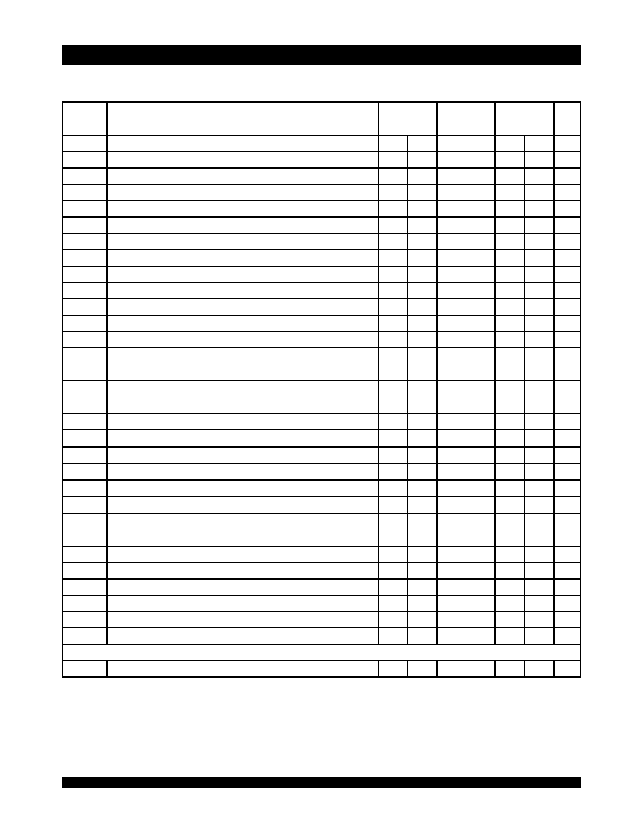
Pin Configuration
(1,2,3,4)
(con't.)
NOTES:
1. All V
DD
pins must be connected to 3.3V power supply.
2. All V
DDQ
pins must be connected to appropriate power supply: 3.3V if OPT pin for that port is set to V
IH
(3.3V), and 2.5V if OPT pin for that port is set to V
IL
(0V).
3. All V
SS
pins must be connected to ground supply.
4. Package body is approximately 28mm x 28mm x 3.5mm.
5. This package code is used to reference the package diagram.
6. This text does not indicate orientation of the actual part-marking.
1
2
3
4
5
6
7
8
9
10
11
12
13
14
15
16
17
18
19
20
21
22
23
24
25
26
27
28
29
30
31
32
33
34
35
36
37
38
39
40
41
42
43
44
45
46
47
48
49
50
51
52
53
54
55
56
57
58
59
60
61
62
63
64
65
66
67
68
69
70
71
72
73
74
75
76
77
78
79
80
81
82
83
84
85
86
87
88
89
90
91
92
93
94
95
96
97
98
99
100
101
102
103
104
156
155
154
153
152
151
150
149
148
147
146
145
144
143
142
141
140
139
138
137
136
135
134
133
132
131
130
129
128
127
126
125
124
123
122
121
120
119
118
117
116
115
114
113
112
111
110
109
108
107
106
105
20
8
20
7
20
6
20
5
20
4
20
3
20
2
20
1
20
0
19
9
19
8
19
7
19
6
19
5
19
4
19
3
19
2
19
1
19
0
18
9
18
8
18
7
18
6
18
5
18
4
18
3
18
2
18
1
18
0
17
9
17
8
17
7
17
6
17
5
17
4
17
3
17
2
17
1
17
0
16
9
16
8
16
7
16
6
16
5
16
4
16
3
16
2
16
1
16
0
15
9
15
8
15
7
70V7519DR
DR-208
(5)
208-Pin PQFP
Top View
(6)
I/O
19L
I/O
19R
I/O
20L
I/O
20R
V
DDQL
V
SS
I/O
21L
I/O
21R
I/O
22L
I/O
22R
V
DDQR
V
SS
I/O
23L
I/O
23R
I/O
24L
I/O
24R
V
DDQL
V
SS
I/O
25L
I/O
25R
I/O
26L
I/O
26R
V
DDQR
V
SS
V
DD
V
DD
V
SS
V
SS
V
DDQL
V
SS
I/O
27R
I/O
27L
I/O
28R
I/O
28L
V
DDQR
V
SS
I/O
29R
I/O
29L
I/O
30R
I/O
30L
V
DDQL
V
SS
I/O
31R
I/O
31L
I/O
32R
I/O
32L
V
DDQR
V
SS
I/O
33R
I/O
33L
I/O
34R
I/O
34L
V
S
S
V
D
D
Q
L
I/O
3
5R
I/O
35
L
P
L/
F
T
R
T
M
S
T
C
K
T
R
S
T
N
C
N
C
B
A
5R
B
A
4R
B
A
3R
B
A
2R
B
A
1R
B
A
0R
A
1
1R
A
1
0R
A
9R
A
8R
A
7R
B
E
3R
B
E
2R
B
E
1R
B
E
0R
C
E
1R
C
E
0R
V
D
D
V
D
D
V
S
S
V
S
S
C
LK
R
O
E
R
R
/
W
R
A
D
S
R
C
N
T
E
N
R
R
E
P
E
A
T
R
A
6R
A
5R
A
4R
A
3R
A
2R
A
1R
A
0R
V
D
D
V
S
S
V
S
S
O
P
T
R
I/O
0
L
I/O
0R
V
D
D
Q
L
V
S
S
I/O
16L
I/O
16R
I/O
15L
I/O
15R
V
SS
V
DDQL
I/O
14L
I/O
14R
I/O
13L
I/O
13R
V
SS
V
DDQR
I/O
12L
I/O
12R
I/O
11L
I/O
11R
V
SS
V
DDQL
I/O
10L
I/O
10R
I/O
9L
I/O
9R
V
SS
V
DDQR
V
DD
V
DD
V
SS
V
SS
V
SS
V
DDQL
I/O
8R
I/O
8L
I/O
7R
I/O
7L
V
SS
V
DDQR
I/O
6R
I/O
6L
I/O
5R
I/O
5L
V
SS
V
DDQL
I/O
4R
I/O
4L
I/O
3R
I/O
3L
V
SS
V
DDQR
I/O
2R
I/O
2L
I/O
1R
I/O
1L
V
S
S
V
D
D
Q
R
I/O
18
R
I/O
18
L
V
S
S
P
L/
F
T
L
T
D
I
T
D
O
N
C
N
C
B
A
5L
B
A
4L
B
A
3L
B
A
2L
B
A
1L
B
A
0L
A
11L
A
10L
A
9L
A
8L
A
7L
B
E
3L
B
E
2L
B
E
1L
B
E
0L
C
E
1
L
C
E
0
L
V
D
D
V
D
D
V
S
S
V
S
S
C
LK
L
O
E
L
R
/
W
L
A
D
S
L
C
N
T
E
N
L
R
E
P
E
A
T
L
A
6L
A
5L
A
4L
A
3L
A
2L
A
1L
A
0L
V
D
D
V
D
D
V
S
S
O
P
T
L
I/O
17
L
I/O
17
R
V
D
D
Q
R
V
S
S
5618 drw 02a
,
11/08/01

6.42
IDT70V7519S
High-Speed 256K x 36 Synchronous Bank-Switchable Dual-Port Static RAM Industrial and Commercial Temperature Ranges
5
Pin Names
Left Port
Right Port
Names
CE
0L
,
CE
1L
CE
0R
,
CE
1R
Chip Enables
R/
W
L
R/
W
R
Read/Write Enable
OE
L
OE
R
Output Enable
BA
0L
- BA
5L
BA
0R
- BA
5R
Bank Address
(4)
A
0L
- A
11L
A
0R
- A
11R
Address
I/O
0L
- I/O
35L
I/O
0R
- I/O
35R
Data Input/Output
CLK
L
CLK
R
Clock
PL/
FT
L
PL/
FT
R
Pipeline/Flow-Through
ADS
L
ADS
R
Address Strobe Enable
CNTEN
L
CNTEN
R
Counter Enable
REPEAT
L
REPEAT
R
Counter Repeat
(3)
BE
0L
-
BE
3L
BE
0R
-
BE
3R
Byte Enables (9-bit bytes)
V
DDQL
V
DDQR
Power (I/O Bus) (3.3V or 2.5V)
(1)
OPT
L
OPT
R
Option for selecting V
DDQX
(1,2)
V
DD
Power (3.3V)
(1)
V
SS
Ground (0V)
TDI
Test Data Input
TDO
Test Data Output
TCK
Test Logic Clock (10MHz)
TMS
Test Mode Select
TRST
Reset (Initialize TAP Controller)
5618 tbl 01
NOTES:
1. V
DD
, OPT
X
, and V
DDQX
must be set to appropriate operating levels prior to
applying inputs on the I/Os and controls for that port.
2. OPT
X
selects the operating voltage levels for the I/Os and controls on that port.
If OPT
X
is set to VIH (3.3V), then that port's I/Os and controls will operate at 3.3V
levels and V
DDQX
must be supplied at 3.3V. If OPT
X
is set to VIL (0V), then that
port's I/Os and address controls will operate at 2.5V levels and V
DDQX
must be
supplied at 2.5V. The OPT pins are independent of one another--both ports can
operate at 3.3V levels, both can operate at 2.5V levels, or either can operate
at 3.3V with the other at 2.5V.
3. When
REPEAT
X
is asserted, the counter will reset to the last valid address loaded
via
ADS
X
.
4. Accesses by the ports into specific banks are controlled by the bank address
pins under the user's direct control: each port can access any bank of memory
with the shared array that is not currently being accessed by the opposite port
(i.e., BA
0L
- BA
5L
BA
0R
- BA
5R
). In the event that both ports try to access the
same bank at the same time, neither access will be valid, and data at the two
specific addresses targeted by the ports within that bank may be corrupted (in
the case that either or both ports are writing) or may result in invalid output (in
the case that both ports are trying to read).
6.42
6
IDT70V7519S
High-Speed 256K x 36 Synchronous Bank-Switchable Dual-Port Static RAM Industrial and Commercial Temperature Ranges
NOTES:
1. "H" = V
IH,
"L" = V
IL,
"X" = Don't Care.
2.
ADS, CNTEN, REPEAT are set as appropriate for address access. Refer to Truth Table II for details.
3.
OE is an asynchronous input signal.
4. It is possible to read or write any combination of bytes during a given access. A few representative samples have been illustrated here.
Truth Table IRead/Write and Enable Control
(1,2,3,4)
OE
3
CLK
CE
0
CE
1
BE
3
BE
2
BE
1
BE
0
R/
W
Byte 3
I/O
27-35
Byte 2
I/O
18-26
Byte 1
I/O
9-17
Byte 0
I/O
0-8
MODE
X
H
X
X
X
X
X
X
High-Z
High-Z
High-Z
High-Z
Deselected≠Power Down
X
X
L
X
X
X
X
X
High-Z
High-Z
High-Z
High-Z
Deselected≠Power Down
X
L
H
H
H
H
H
X
High-Z
High-Z
High-Z
High-Z
All Bytes Deselected
X
L
H
H
H
H
L
L
High-Z
High-Z
High-Z
D
IN
Write to Byte 0 Only
X
L
H
H
H
L
H
L
High-Z
High-Z
D
IN
High-Z
Write to Byte 1 Only
X
L
H
H
L
H
H
L
High-Z
D
IN
High-Z
High-Z
Write to Byte 2 Only
X
L
H
L
H
H
H
L
D
IN
High-Z
High-Z
High-Z
Write to Byte 3 Only
X
L
H
H
H
L
L
L
High-Z
High-Z
D
IN
D
IN
Write to Lower 2 Bytes Only
X
L
H
L
L
H
H
L
D
IN
D
IN
High-Z
High-Z
Write to Upper 2 bytes Only
X
L
H
L
L
L
L
L
D
IN
D
IN
D
IN
D
IN
Write to All Bytes
L
L
H
H
H
H
L
H
High-Z
High-Z
High-Z
D
OUT
Read Byte 0 Only
L
L
H
H
H
L
H
H
High-Z
High-Z
D
OUT
High-Z
Read Byte 1 Only
L
L
H
H
L
H
H
H
High-Z
D
OUT
High-Z
High-Z
Read Byte 2 Only
L
L
H
L
H
H
H
H
D
OUT
High-Z
High-Z
High-Z
Read Byte 3 Only
L
L
H
H
H
L
L
H
High-Z
High-Z
D
OUT
D
OUT
Read Lower 2 Bytes Only
L
L
H
L
L
H
H
H
D
OUT
D
OUT
High-Z
High-Z
Read Upper 2 Bytes Only
L
L
H
L
L
L
L
H
D
OUT
D
OUT
D
OUT
D
OUT
Read All Bytes
H
X
X
X
X
X
X
X
X
High-Z
High-Z
High-Z
High-Z
Outputs Disabled
5618 tbl 02
Truth Table IIAddress and Address Counter Control
(1,2,7)
NOTES:
1. "H" = V
IH,
"L" = V
IL,
"X" = Don't Care.
2. Read and write operations are controlled by the appropriate setting of R/
W, CE
0
, CE
1
,
BEn and OE.
3. Outputs configured in flow-through output mode: if outputs are in pipelined mode the data out will be delayed by one cycle.
4.
ADS and REPEAT are independent of all other memory control signals including CE
0
, CE
1
and
BEn
5. The address counter advances if
CNTEN = V
IL
on the rising edge of CLK, regardless of all other memory control signals including
CE
0
, CE
1
,
BEn.
6. When
REPEAT is asserted, the counter will reset to the last valid address loaded via ADS. This value is not set at power-up: a known location should be loaded
via
ADS during initialization if desired. Any subsequent ADS access during operations will update the REPEAT address location.
7. The counter includes bank address and internal address. The counter will advance across bank boundaries. For example, if the counter is in Bank 0, at address
FFFh, and is advanced one location, it will move to address 0h in Bank 1. By the same token, the counter at FFFh in Bank 63 will advance to 0h in Bank 0. Refer
to Timing Waveform of Counter Repeat, page 18. Care should be taken during operation to avoid having both counters point to the same bank (i.e., ensure BA
0L
- BA
5L
BA
0R
- BA
5R
), as this condition will invalidate the access for both ports. Please refer to the functional description on page 19 for details.
Address
Previous
Address
Addr
Used
CLK
ADS
CNTEN REPEAT
(6)
I/O
(3)
MODE
An
X
An
L
(4)
X
H
D
I/O
(n)
External Address Used
X
An
An + 1
H
L
(5)
H
D
I/O
(n+1)
Counter Enabled--Internal Address generation
X
An + 1
An + 1
H
H
H
D
I/O
(n+1)
External Addre ss Blocked--Counter disab led (An + 1 reused)
X
X
An
X
X
L
(4)
D
I/O
(0)
Counter Set to last valid
ADS load
5618 tbl 03
6.42
IDT70V7519S
High-Speed 256K x 36 Synchronous Bank-Switchable Dual-Port Static RAM Industrial and Commercial Temperature Ranges
7
Recommended Operating
Temperature and Supply Voltage
(1)
Recommended DC Operating
Conditions with V
DDQ
at 2.5V
Absolute Maximum Ratings
(1)
NOTES:
1. Undershoot of V
IL >
-1.5V for pulse width less than 10ns is allowed.
2. V
TERM
must not exceed V
DDQ
+ 100mV.
3. To select operation at 2.5V levels on the I/Os and controls of a given port, the
OPT pin for that port must be set to V
IL
(0V), and V
DDQX
for that port must be supplied
as indicated above.
NOTES:
1. Stresses greater than those listed under ABSOLUTE MAXIMUM RATINGS may
cause permanent damage to the device. This is a stress rating only and functional
operation of the device at these or any other conditions above those indicated
in the operational sections of this specification is not implied. Exposure to absolute
maximum rating conditions for extended periods may affect reliability.
2. V
TERM
must not exceed V
DD
+ 150mV for more than 25% of the cycle time or
4ns maximum, and is limited to < 20mA for the period of V
TERM
> V
DD
+ 150mV.
NOTE:
1. This is the parameter T
A
. This is the "instant on" case temperature.
Grade
Ambient
Temperature
GND
V
DD
Commercial
0
O
C to +70
O
C
0V
3.3V
+
150mV
Industrial
-40
O
C to +85
O
C
0V
3.3V
+
150mV
5618 tbl 04
Symbol
Parameter
Min.
Typ.
Max.
Unit
V
DD
Core Supply Voltage
3.15
3.3
3.45
V
V
DDQ
I/O Supply Voltage
(3)
2.4
2.5
2.6
V
V
SS
Ground
0
0
0
V
V
IH
Input High Voltage
(Address & Control Inputs)
1.7
____
V
DDQ
+ 100mV
(2)
V
V
IH
Input High Voltage - I/O
(3)
1.7
____
V
DDQ
+ 100mV
(2)
V
V
IL
Input Low Voltage
-0.3
(1)
____
0.7
V
5618 tbl 05a
Symbol
Rating
Commercial
& Industrial
Unit
V
TERM
(2)
Terminal Voltage
with Respect to
GND
-0.5 to +4.6
V
T
BIAS
Temperature
Under Bias
-55 to +125
o
C
T
STG
Storage
Temperature
-65 to +150
o
C
I
OUT
DC Output Current
50
mA
5618 tbl 06
Recommended DC Operating
Conditions with V
DDQ
at 3.3V
NOTES:
1. Undershoot of V
IL >
-1.5V for pulse width less than 10ns is allowed.
2. V
TERM
must not exceed V
DDQ
+ 150mV.
3. To select operation at 3.3V levels on the I/Os and controls of a given port, the
OPT pin for that port must be set to V
IH
(3.3V), and V
DDQX
for that port must be
supplied as indicated above.
Symbol
Parameter
Min.
Typ.
Max.
Unit
V
DD
Core Supply Voltage
3.15
3.3
3.45
V
V
DDQ
I/O Supply Voltage
(3)
3.15
3.3
3.45
V
V
SS
Ground
0
0
0
V
V
IH
Input High Voltage
(Address & Control Inputs)
(3)
2.0
____
V
DDQ
+ 150mV
(2)
V
V
IH
Input High Voltage - I/O
(3)
2.0
____
V
DDQ
+ 150mV
(2)
V
V
IL
Input Low Voltage
-0.3
(1)
____
0.8
V
5618 tbl 05b
6.42
8
IDT70V7519S
High-Speed 256K x 36 Synchronous Bank-Switchable Dual-Port Static RAM Industrial and Commercial Temperature Ranges
DC Electrical Characteristics Over the Operating
Temperature and Supply Voltage Range
(V
DD
= 3.3V ± 150mV)
NOTES:
1. At V
DD
< 2.0V leakages are undefined.
2. V
DDQ
is selectable (3.3V/2.5V) via OPT pins. Refer to p.5 for details.
Symbol
Parameter
Test Conditions
70V7519S
Unit
Min.
Max.
|I
LI
|
Input Leakage Current
(1)
V
DDQ
= Max., V
IN
= 0V to V
DDQ
___
10
µ A
|I
LO
|
Output Leakage Current
(1)
CE
0
= V
IH
or CE
1
= V
IL
, V
OUT
= 0V to V
DDQ
___
10
µ A
V
OL
(3.3V)
Output Low Voltage
(2)
I
OL
= +4mA, V
DDQ
= Min.
___
0.4
V
V
OH
(3.3V)
Output High Voltage
(2)
I
OH
= -4mA, V
DDQ
= Min.
2.4
___
V
V
OL
(2.5V)
Output Low Voltage
(2)
I
OL
= +2mA, V
DDQ
= Min.
___
0.4
V
V
OH
(2.5V)
Output High Voltage
(2)
I
OH
= -2mA, V
DDQ
= Min.
2.0
___
V
5618 tbl 08
NOTES:
1. These parameters are determined by device characterization, but are not
production tested.
2. 3dV references the interpolated capacitance when the input and output switch
from 0V to 3V or from 3V to 0V.
3. C
OUT
also references C
I/O
.
Capacitance
(1)
(T
A
= +25∞C, F = 1.0MH
Z
) PQFP ONLY
Symbol
Parameter
Conditions
(2)
Max.
Unit
C
IN
Input Capacitance
V
IN
= 3dV
8
pF
C
OUT
(3)
Output Capacitance
V
OUT
= 3dV
10.5
pF
5618 tbl 07

6.42
IDT70V7519S
High-Speed 256K x 36 Synchronous Bank-Switchable Dual-Port Static RAM Industrial and Commercial Temperature Ranges
9
DC Electrical Characteristics Over the Operating
Temperature and Supply Voltage Range
(5)
(V
DD
= 3.3V ± 150mV)
NOTES:
1. At f = f
MAX
, address and control lines (except Output Enable) are cycling at the maximum frequency clock cycle of 1/t
CYC
, using "AC TEST CONDITIONS" at input
levels of GND to 3V.
2. f = 0 means no address, clock, or control lines change. Applies only to input at CMOS level standby.
3. Port "A" may be either left or right port. Port "B" is the opposite from port "A".
4. V
DD
= 3.3V, T
A
= 25∞C for Typ, and are not production tested. I
DD DC
(f=0)
= 120mA (Typ).
5.
CE
X
= V
IL
means
CE
0X
= V
IL
and CE
1X
= V
IH
CE
X
= V
IH
means
CE
0X
= V
IH
or CE
1X
= V
IL
CE
X
< 0.2V means
CE
0X
< 0.2V and CE
1X
> V
CC
- 0.2V
CE
X
> V
CC
- 0.2V means
CE
0X
> V
CC
- 0.2V or CE
1X
< 0.2V
"X" represents "L" for left port or "R" for right port.
70V 7519S200
(7)
Com 'l O nly
70V 7519S166
(6)
Com 'l
& Ind
70V 7519S133
Com 'l
& Ind
Sym bol
P aram eter
Test Condition
Version
Typ.
(4)
M ax.
Typ.
(4)
M ax.
Typ.
(4)
M ax.
Unit
I
DD
Dy nam ic O p e rating
C urre nt (B o th
P o rts A c tiv e )
CE
L
and
CE
R
= V
IL
,
O utp uts Dis ab le d ,
f = f
M A X
(1 )
C OM 'L
S
815
950
675
790
550
645
m A
IND
S
____
____
675
830
550
675
I
S B1
S tand b y C urre nt
(B o th P o rts - TTL
Le v e l Inp uts )
CE
L
=
CE
R
= V
IH
f = f
M A X
(1 )
C OM 'L
S
340
410
275
340
250
295
m A
IND
S
____
____
275
355
250
310
I
S B2
S tand b y C urre nt
(One P o rt - TTL
Le v e l Inp uts )
CE
"A "
= V
IL
and
CE
"B "
= V
IH
(3 )
A c tiv e P o rt Outp uts D isab le d ,
f= f
M A X
(1 )
C OM 'L
S
690
770
515
640
460
520
m A
IND
S
____
____
515
660
460
545
I
S B3
F ull S tand b y C urre nt
(B o th P o rts - C M O S
Le v e l Inp uts )
B o th P o rts
CE
L
and
CE
R
> V
DD
- 0.2V, V
IN
> V
DD
- 0.2V
o r V
IN
< 0.2 V, f = 0
(2 )
C OM 'L
S
10
30
10
30
10
30
m A
IND
S
____
____
10
40
10
40
I
S B4
F ull S tand b y C urre nt
(One P o rt - CM OS
Le v e l Inp uts )
CE
"A "
< 0.2V and
CE
"B "
> V
DD
- 0.2V
(3 )
V
IN
> V
DD
- 0.2V o r V
IN
< 0.2V
A c tiv e P o rt, O utp uts D isab le d , f = f
M A X
(1 )
C OM 'L
S
690
770
515
640
460
520
m A
IND
S
____
____
515
660
460
545
5618 tb l 0 9
6. 166MHz Industrial Temperature not available in BF-208 package.
7. This speed grade available when V
DDQ
= 3.3.V for a specific port (i.e., OPTx = V
IH
). This speed grade available in BC-256 package only.

6.42
10
IDT70V7519S
High-Speed 256K x 36 Synchronous Bank-Switchable Dual-Port Static RAM Industrial and Commercial Temperature Ranges
AC Test Conditions
(V
DDQ
- 3.3V/2.5V)
Figure 1. AC Output Test load.
Figure 2. Output Test Load
(For t
CKLZ
, t
CKHZ
, t
OLZ
, and t
OHZ
).
*Including scope and jig.
Figure 3. Typical Output Derating (Lumped Capacitive Load).
Input Pulse Levels (Address & Controls)
Input Pulse Levels (I/Os)
Input Rise/Fall Times
Input Timing Reference Levels
Output Reference Levels
Output Load
GND to 3
.
0V/GND to 2.4V
GND to 3.0V/GND to 2.4V
2ns
1.5V/1.25V
1.5V/1.25V
Figures 1 and 2
5618 tbl 10
1.5V/1.25
50
50
5618 drw 03
10pF
(Tester)
DATA
OUT
,
5618 drw 04
590
5pF*
435
3.3V
DATA
OUT
,
833
5pF*
770
2.5V
DATA
OUT
,
-1
1
2
3
4
5
6
7
20.5
30
50
80
100
200
10.5pF is the I/O capacitance of this
device, and 10pF is the AC Test Load
Capacitance.
Capacitance (pF)
tCD
(Typical, ns)
5618 drw 05
∑
∑
∑
∑
,
6.42
IDT70V7519S
High-Speed 256K x 36 Synchronous Bank-Switchable Dual-Port Static RAM Industrial and Commercial Temperature Ranges
11
AC Electrical Characteristics Over the Operating Temperature Range
(Read and Write Cycle Timing)
(2,3)
(V
DD
= 3.3V ± 150mV, T
A
= 0∞C to +70∞C)
NOTES:
1. The Pipelined output parameters (t
CYC2
, t
CD2
) apply to either or both left and right ports when
FT/PIPE
X
= V
IH
. Flow-through parameters (t
CYC1
, t
CD1
) apply when
FT/PIPE
X
= V
IL
for that port.
2. All input signals are synchronous with respect to the clock except for the asynchronous Output Enable (
OE) and FT/PIPE. FT/PIPE should be treated as a
DC signal, i.e. steady state during operation.
3. These values are valid for either level of V
DDQ
(3.3V/2.5V). See page 5 for details on selecting the desired operating voltage levels for each port.
70V7519S200
(5)
Com 'l Only
70V7519S166
(3,4)
Com 'l
& Ind
70V7519S133
(3)
Com 'l
& Ind
Sym bol
Param eter
Min.
Max.
Min.
Max.
Min.
Max.
Unit
t
C Y C 1
Clo ck Cycle Time (Flo w-Thro ug h)
(1)
15
____
20
____
25
____
ns
t
C Y C 2
Clo ck Cycle Time (P ip e line d)
(1)
5
____
6
____
7.5
____
ns
t
C H 1
Clo ck Hig h Time (Flo w-Thro ug h)
(1)
5
____
6
____
7
____
ns
t
CL 1
Clo ck Lo w Tim e (Flow-Thro ugh)
(1)
5
____
6
____
7
____
ns
t
C H 2
Clo ck Hig h Time (P ip e line d)
(2)
2.0
____
2.1
____
2.6
____
ns
t
CL 2
Clo ck Lo w Tim e (P ipe line d )
(1)
2.0
____
2.1
____
2.6
____
ns
t
R
Clo ck Rise Time
____
1.5
____
1.5
____
1.5
ns
t
F
Clo ck Fall Time
____
1.5
____
1.5
____
1.5
ns
t
S A
A d dre ss Se tup Tim e
1.5
____
1.7
____
1.8
____
ns
t
H A
A d dre ss Ho ld Tim e
0.5
____
0.5
____
0.5
____
ns
t
S C
Chip E nab le S e tup Time
1.5
____
1.7
____
1.8
____
ns
t
H C
Chip E nab le Ho ld Time
0.5
____
0.5
____
0.5
____
ns
t
S W
R/W S e tup Time
1.5
____
1.7
____
1.8
____
ns
t
H W
R/W Ho ld Time
0.5
____
0.5
____
0.5
____
ns
t
S D
Inp ut Data S e tup Time
1.5
____
1.7
____
1.8
____
ns
t
H D
Input Data Ho ld Tim e
0.5
____
0.5
____
0.5
____
ns
t
SA D
ADS Se tup Time
1.5
____
1.7
____
1.8
____
ns
t
HA D
ADS Ho ld Time
0.5
____
0.5
____
0.5
____
ns
t
SC N
CNTEN Se tup Time
1.5
____
1.7
____
1.8
____
ns
t
HC N
CNTEN Ho ld Time
0.5
____
0.5
____
0.5
____
ns
t
S R P T
REPEAT Se tup Time
1.5
____
1.7
____
1.8
____
ns
t
H R P T
REPEAT Ho ld Time
0.5
____
0.5
____
0.5
____
ns
t
OE
Outp ut Enab le to Data Valid
____
4.0
____
4.0
____
4.2
ns
t
OL Z
O utp ut Enab le to O utp ut Lo w-Z
0.5
____
0.5
____
0.5
____
ns
t
O H Z
Outp ut Enab le to O utp ut Hig h-Z
1
3.4
1
3.6
1
4.2
ns
t
C D 1
Clo ck to Data Valid (Flo w-Thro ug h)
(1)
____
10
____
12
____
15
ns
t
C D 2
Clo ck to Data Valid (Pip e lined )
(1)
____
3.4
____
3.6
____
4.2
ns
t
D C
Data Output Ho ld A fte r Clo ck Hig h
1
____
1
____
1
____
ns
t
C K H Z
Clo ck Hig h to O utp ut Hig h-Z
1
3.4
1
3.6
1
4.2
ns
t
C KL Z
Clo ck Hig h to O utp ut Lo w-Z
0.5
____
0.5
____
0.5
____
ns
Port-to-Port Delay
t
CO
Clo ck-to -Clo ck O ffse t
5.0
____
6.0
____
7.5
____
ns
5 618 tb l 11
4. 166MHz Industrial Temperature not available in BF-208 package.
5. This speed grade available when V
DDQ
= 3.3.V for a specific port (i.e., OPTx = V
IH
). This speed grade available in BC-256 package only.

6.42
12
IDT70V7519S
High-Speed 256K x 36 Synchronous Bank-Switchable Dual-Port Static RAM Industrial and Commercial Temperature Ranges
An
An + 1
An + 2
An + 3
t
CYC2
t
CH2
t
CL2
R/
W
ADDRESS
CE
0
CLK
CE
1
BE
n
(3)
DATA
OUT
OE
t
CD2
t
CKLZ
Qn
Qn + 1
Qn + 2
t
OHZ
t
OLZ
t
OE
5618 drw 06
(1)
(1)
t
SC
t
HC
t
SB
t
HB
t
SW
t
HW
t
SA
t
HA
t
DC
t
SC
t
HC
t
SB
t
HB
(4)
(1 Latency)
(5)
(5)
Timing Waveform of Read Cycle for Pipelined Operation
(ADS Operation) (FT/PIPE
'X'
= V
IH
)
(2)
NOTES:
1.
OE is asynchronously controlled; all other inputs are synchronous to the rising clock edge.
2.
ADS = V
IL
,
CNTEN and REPEAT = V
IH
.
3. The output is disabled (High-Impedance state) by
CE
0
= V
IH
, CE
1
= V
IL
,
BE
n
= V
IH
following the next rising edge of the clock. Refer to
Truth Table 1.
4. Addresses do not have to be accessed sequentially since
ADS = V
IL
constantly loads the address on the rising edge of the CLK; numbers
are for reference use only.
5. If
BE
n
was HIGH, then the appropriate Byte of DATA
OUT
for Qn + 2 would be disabled (High-Impedance state).
6. "x" denotes Left or Right port. The diagram is with respect to that port.
Timing Waveform of Read Cycle for Flow-through Output
(FT/PIPE
"X"
= V
IL
)
(2,6)
An
An + 1
An + 2
An + 3
t
CYC1
t
CH1
t
CL1
R/
W
ADDRESS
DATA
OUT
CE
0
CLK
OE
t
SC
t
HC
t
CD1
t
CKLZ
Qn
Qn + 1
Qn + 2
t
OHZ
t
OLZ
t
OE
t
CKHZ
5618 drw 07
(5)
(1)
CE
1
BE
n
(3)
t
SB
t
HB
t
SW
t
HW
t
SA
t
HA
t
DC
t
DC
(4)
t
SC
t
HC
t
SB
t
HB
(5)

6.42
IDT70V7519S
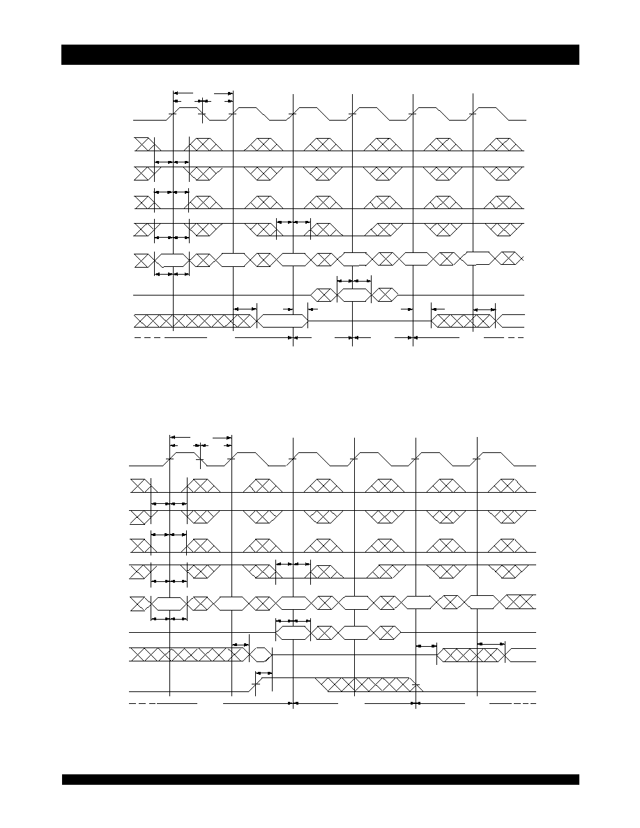
High-Speed 256K x 36 Synchronous Bank-Switchable Dual-Port Static RAM Industrial and Commercial Temperature Ranges
13
t
SC
t
HC
CE
0(B1)
ADDRESS
(B1)
A
0
A
1
A
2
A
3
A
4
A
5
t
SA
t
HA
CLK
Q
0
Q
1
Q
3
DATA
OUT(B1)
t
CH2
t
CL2
t
CYC2
ADDRESS
(B2)
A
0
A
1
A
2
A
3
A
4
A
5
t
SA
t
HA
CE
0(B2)
DATA
OUT(B2)
Q
2
Q
4
t
CD2
t
CD2
t
CKHZ
t
CD2
t
CKLZ
t
DC
t
CKHZ
t
CD2
t
CKLZ
t
SC
t
HC
t
CKHZ
t
CKLZ
t
CD2
A
6
A
6
t
DC
t
SC
t
HC
t
SC
t
HC
5618 drw 08
Timing Waveform of a Multi-Device Pipelined Read
(1,2)
NOTES:
1. B1 Represents Device #1; B2 Represents Device #2. Each Device consists of one IDT70V7519 for this waveform,
and are setup for depth expansion in this example. ADDRESS
(B1)
= ADDRESS
(B2)
in this situation.
2.
BE
n
,
OE, and ADS = V
IL
; CE
1(B1)
, CE
1(B2)
, R/
W, CNTEN, and REPEAT = V
IH
.
Timing Waveform of a Multi-Device Flow-Through Read
(1,2)
t
SC
t
HC
CE
0(B1)
ADDRESS
(B1)
A
0
A
1
A
2
A
3
A
4
A
5
t
SA
t
HA
CLK
5618 drw 09
D
0
D
3
t
CD1
t
CKLZ
t
CKHZ
(1)
(1)
D
1
DATA
OUT(B1)
t
CH1
t
CL1
t
CYC1
(1)
ADDRESS
(B2)
A
0
A
1
A
2
A
3
A
4
A
5
t
SA
t
HA
CE
0(B2)
DATA
OUT(B2)
D
2
D
4
t
CD1
t
CD1
t
CKHZ
t
DC
t
CD1
t
CKLZ
t
SC
t
HC
(1)
t
CKHZ
(1)
t
CKLZ
(1)
t
CD1
A
6
A
6
t
DC
t
SC
t
HC
t
SC
t
HC
D
5
t
CD1
t
CKLZ
(1)
t
CKHZ
(1)

6.42
14
IDT70V7519S
High-Speed 256K x 36 Synchronous Bank-Switchable Dual-Port Static RAM Industrial and Commercial Temperature Ranges
CLK
"A"
R/
W
"A"
BANK ADDRESS
AND ADDRESS
"A"
DATA
IN"A"
CLK
"B"
R/
W
"B"
BANK ADDRESS
AND ADDRESS
"B"
DATA
OUT"B"
t
SW
t
HW
t
SA
t
HA
t
SD
t
HD
t
SW
t
HW
t
SA
t
HA
t
CD2
Dn
An
An
Dn
5618 drw 10
t
DC
t
CO
(3)
Timing Waveform of Port A Write to Pipelined Port B Read
(1,2,4)
NOTES:
1.
CE
0
,
BE
n
, and
ADS = V
IL
; CE
1
,
CNTEN, and REPEAT = V
IH
.
2.
OE = V
IL
for Port "B", which is being read from.
OE = V
IH
for Port "A", which is being written to.
3. If t
CO
< minimum specified, then operations from both ports are INVALID. If t
CO
minimum, then data from Port "B" read is available on first Port "B" clock cycle
(ie, time from write to valid read on opposite port will be t
CO
+ t
CYC2
+ t
CD2
).
4. All timing is the same for Left and Right ports. Port "A" may be either Left or Right port. Port "B" is the opposite of Port "A"
Timing Waveform with Port-to-Port Flow-Through Read
(1,2,4)
DATA
IN "A"
CLK
"B"
R/
W
"B"
BANK ADDRESS
AND ADDRESS
"A"
R/
W
"A"
CLK
"A"
BANK ADDRESS
AND ADDRESS
"B"
An
An
Dn
t
DC
DATA
OUT "B"
5618 drw 11
Dn
t
SW
t
HW
t
SA
t
HA
t
SD
t
HD
t
HW
t
CD1
t
CO
(3)
t
DC
t
SA
t
SW
t
HA
NOTES:
1.
CE
0
,
BEn, and ADS = V
IL
; CE
1
,
CNTEN, and REPEAT = V
IH
.
2.
OE = V
IL
for the Right Port, which is being read from.
OE = V
IH
for the Left Port, which is being written to.
3. If t
CO
< minimum specified, then operations from both ports are INVALID. If t
CO
minimum, then data from Port "B" read is available on first Port "B" clock cycle
(i.e., time from write to valid read on opposite port will be t
CO
+ t
CD1
).
4. All timing is the same for both left and right ports. Port "A" may be either left or right port. Port "B" is the opposite of Port "A".
6.42
IDT70V7519S
High-Speed 256K x 36 Synchronous Bank-Switchable Dual-Port Static RAM Industrial and Commercial Temperature Ranges
15
R/
W
ADDRESS
An
An +1
An + 2
An + 2
An + 3
An + 4
DATA
IN
Dn + 2
CE
0
CLK
5618 drw 12
Qn
Qn + 3
DATA
OUT
CE
1
BE
n
t
CD2
t
CKHZ
t
CKLZ
t
CD2
t
SC
t
HC
t
SB
t
HB
t
SW
t
HW
t
SA
t
HA
t
CH2
t
CL2
t
CYC2
READ
NOP
READ
t
SD
t
HD
(3)
(1)
t
SW
t
HW
WRITE
(4)
Timing Waveform of Pipelined Read-to-Write-to-Read
(OE = V
IL
)
(2)
NOTES:
1. Output state (High, Low, or High-impedance) is determined by the previous cycle control signals.
2.
CE
0
,
BE
n
, and
ADS = V
IL
; CE
1
,
CNTEN, and REPEAT = V
IH
. "NOP" is "No Operation".
3. Addresses do not have to be accessed sequentially since
ADS = V
IL
constantly loads the address on the rising edge of the CLK; numbers
are for reference use only.
4. "NOP" is "No Operation." Data in memory at the selected address may be corrupted and should be re-written to guarantee data integrity.
R/
W
ADDRESS
An
An +1
An + 2
An + 3
An + 4
An + 5
DATA
IN
Dn + 3
Dn + 2
CE
0
CLK
5618 drw 13
DATA
OUT
Qn
Qn + 4
CE
1
BE
n
OE
t
CH2
t
CL2
t
CYC2
t
CKLZ
t
CD2
t
OHZ
t
CD2
t
SD
t
HD
READ
WRITE
READ
t
SC
t
HC
t
SB
t
HB
t
SW
t
HW
t
SA
t
HA
(3)
(1)
t
SW
t
HW
(4)
Timing Waveform of Pipelined Read-to-Write-to-Read (OE Controlled)
(2)
NOTES:
1. Output state (High, Low, or High-impedance) is determined by the previous cycle control signals.
2.
CE
0
,
BE
n
, and
ADS = V
IL
; CE
1
,
CNTEN, and REPEAT = V
IH
.
3. Addresses do not have to be accessed sequentially since
ADS = V
IL
constantly loads the address on the rising edge of the CLK; numbers are for reference
use only.
4. This timing does not meet requirements for fastest speed grade. This waveform indicates how logically it could be done if timing so allows.

6.42
16
IDT70V7519S
High-Speed 256K x 36 Synchronous Bank-Switchable Dual-Port Static RAM Industrial and Commercial Temperature Ranges
Timing Waveform of Flow-Through Read-to-Write-to-Read (OE = V
IL
)
(2)
Timing Waveform of Flow-Through Read-to-Write-to-Read (OE Controlled)
(2)
NOTES:
1. Output state (High, Low, or High-impedance) is determined by the previous cycle control signals.
2.
CE
0
,
BEn, and ADS = V
IL
; CE
1
,
CNTEN, and REPEAT = V
IH
.
3. Addresses do not have to be accessed sequentially since
ADS = V
IL
constantly loads the address on the rising edge of the CLK; numbers are for
reference use only.
4. "NOP" is "No Operation." Data in memory at the selected address may be corrupted and should be re-written to guarantee data integrity.
R/
W
ADDRESS
An
An +1
An + 2
An + 2
An + 3
An + 4
DATA
IN
Dn + 2
CE
0
CLK
5618 drw 14
Qn
DATA
OUT
CE
1
BE
n
t
CD1
Qn + 1
t
CH1
t
CL1
t
CYC1
t
SD
t
HD
t
CD1
t
CD1
t
DC
t
CKHZ
Qn + 3
t
CD1
t
DC
t
SC
t
HC
t
SB
t
HB
t
SW
t
HW
t
SA
t
HA
READ
NOP
READ
t
CKLZ
(3)
(1)
t
SW
t
HW
WRITE
(4)
R/
W
ADDRESS
An
An +1
An + 2
An + 3
An + 4
An + 5
(3)
DATA
IN
Dn + 2
CE
0
CLK
5618 drw 15
Qn
DATA
OUT
CE
1
BE
n
t
CD1
t
CH1
t
CL1
t
CYC1
t
SD
t
HD
t
CD1
t
DC
Qn + 4
t
CD1
t
DC
t
SC
t
HC
t
SB
t
HB
t
SW
t
HW
t
SA
t
HA
READ
WRITE
READ
t
CKLZ
(1)
Dn + 3
t
OHZ
t
SW
t
HW
OE
t
OE

6.42
IDT70V7519S
High-Speed 256K x 36 Synchronous Bank-Switchable Dual-Port Static RAM Industrial and Commercial Temperature Ranges
17
ADDRESS
An
CLK
DATA
OUT
Qx - 1
(2)
Qx
Qn
Qn + 2
(2)
Qn + 3
ADS
CNTEN
t
CYC2
t
CH2
t
CL2
5618 drw 16
t
SA
t
HA
t
SAD
t
HAD
t
CD2
t
DC
READ
EXTERNAL
ADDRESS
READ WITH COUNTER
COUNTER
HOLD
t
SAD
t
HAD
t
SCN
t
HCN
READ
WITH
COUNTER
Qn + 1
Timing Waveform of Pipelined Read with Address Counter Advance
(1)
NOTES:
1.
CE
0
,
OE, BEn = V
IL
; CE
1
, R/
W, and REPEAT = V
IH
.
2. If there is no address change via
ADS = V
IL
(loading a new address) or
CNTEN = V
IL
(advancing the address), i.e.
ADS = V
IH
and
CNTEN = V
IH
, then
the data output remains constant for subsequent clocks.
Timing Waveform of Flow-Through Read with Address Counter Advance
(1)
ADDRESS
An
CLK
DATA
OUT
Qx
(2)
Qn
Qn + 1
Qn + 2
Qn + 3
(2)
Qn + 4
ADS
CNTEN
t
CYC1
t
CH1
t
CL1
5618 drw 17
t
SA
t
HA
t
SAD
t
HAD
READ
EXTERNAL
ADDRESS
READ WITH COUNTER
COUNTER
HOLD
t
CD1
t
DC
t
SAD
t
HAD
t
SCN
t
HCN
READ
WITH
COUNTER

6.42
18
IDT70V7519S
High-Speed 256K x 36 Synchronous Bank-Switchable Dual-Port Static RAM Industrial and Commercial Temperature Ranges
Timing Waveform of Write with Address Counter Advance
(Flow-through or Pipelined Inputs)
(1,6)
NOTES:
1.
CE
0
,
BE
n
, and R/
W = V
IL
; CE
1
and
REPEAT = V
IH
.
2. CE
0
,
BE
n
= V
IL
; CE
1
= V
IH
.
3. The "Internal Address" is equal to the "External Address" when
ADS = V
IL
and equals the counter output when
ADS = V
IH
.
4. No dead cycle exists during
REPEAT operation. A READ or WRITE cycle may be coincidental with the counter REPEAT cycle: Address loaded by last valid
ADS load will be accessed. For more information on REPEAT function refer to Truth Table II.
5.
CNTEN = V
IL
advances Internal Address from `An' to `An +1'. The transition shown indicates the time required for the counter to advance. The `An +1'Address is
written to during this cycle.
6. The counter includes bank address and internal address. The counter will advance across bank boundaries. For example, if the counter is in Bank 0, at address
FFFh, and is advanced one location, it will move to address 0h in Bank 1. By the same token, the counter at FFFh in Bank 63 will advance to 0h in Bank 0.
7. For Pipelined Mode user should add 1 cycle latency for outputs as per timing waveform of read cycle for pipelined operations.
ADDRESS
An
CLK
DATA
IN
Dn
Dn + 1
Dn + 1
Dn + 2
ADS
CNTEN
t
CH2
t
CL2
t
CYC2
5618 drw 18
INTERNAL
(3)
ADDRESS
An
(5)
An + 1
An + 2
An + 3
An + 4
Dn + 3
Dn + 4
t
SA
t
HA
t
SAD
t
HAD
WRITE
COUNTER HOLD
WRITE WITH COUNTER
WRITE
EXTERNAL
ADDRESS
WRITE
WITH COUNTER
t
SD
t
HD
t
SCN
t
HCN
Timing Waveform of Counter Repeat for Flow Through Mode
(2,6,7)
ADDRESS
An
t
CYC2
CLK
DATA
IN
R/
W
REPEAT
5618 drw 19
INTERNAL
(3)
ADDRESS
ADS
CNTEN
WRITE TO
ADS
ADDRESS
An
ADVANCE
COUNTER
WRITE TO
An+1
ADVANCE
COUNTER
WRITE TO
An+2
HOLD
COUNTER
WRITE TO
An+2
REPEAT
READ LAST
ADS
ADDRESS
An
DATA
OUT
t
SA
t
HA
,
An
t
SAD
t
HAD
t
SW
t
HW
t
SCN
t
HCN
t
SRPT
t
HRPT
t
SD
t
HD
t
CD1
An+1
An+2
An+2
An
An+1
An+2
An+2
D
0
D
1
D
2
D
3
An
An+1
An+2
An+2
ADVANCE
COUNTER
READ
An+1
ADVANCE
COUNTER
READ
An+2
HOLD
COUNTER
READ
An+2
(4)

6.42
IDT70V7519S
High-Speed 256K x 36 Synchronous Bank-Switchable Dual-Port Static RAM Industrial and Commercial Temperature Ranges
19
Functional Description
The IDT70V7519 is a high-speed 256Kx36 (9 Mbit) synchronous
Bank-Switchable Dual-Ported SRAM organized into 64 independent
4Kx36 banks. Based on a standard SRAM core instead of a traditional true
dual-port memory core, this bank-switchable device offers the benefits of
increased density and lower cost-per-bit while retaining many of the
features of true dual-ports. These features include simultaneous, random
access to the shared array, separate clocks per port, 166 MHz operating
speed, full-boundary counters, and pinouts compatible with the IDT70V3599
(128Kx36) dual-port family.
The two ports are permitted independent, simultaneous access into
separate banks within the shared array. Access by the ports into specific
banks are controlled by the bank address pins under the user's direct
control: each port can access any bank of memory with the shared array
that is not currently being accessed by the opposite port (i.e., BA
0L
- BA
5L
BA
0R
- BA
5R
). In the event that both ports try to access the same bank
at the same time, neither access will be valid, and data at the two specific
addresses targeted by the ports within that bank may be corrupted (in the
case that either or both ports are writing) or may result in invalid output (in
the case that both ports are trying to read).
The IDT70V7519 provides a true synchronous Dual-Port Static RAM
5618 drw 20
IDT70V7519
CE
0
CE
1
CE
1
CE
0
CE
0
CE
1
BA
6
(1)
CE
1
CE
0
V
DD
V
DD
IDT70V7519
IDT70V7519
IDT70V7519
Control Inputs
Control Inputs
Control Inputs
Control Inputs
BE
,
R/
W
,
OE
,
CLK,
ADS
,
REPEAT
,
CNTEN
Figure 4. Depth and Width Expansion with IDT70V7519
interface. Registered inputs provide minimal setup and hold times on
address, data and all critical control inputs.
An asynchronous output enable is provided to ease asynchronous
bus interfacing. Counter enable inputs are also provided to stall the
operation of the address counters for fast interleaved memory applications.
A HIGH on
CE
0
or a LOW on CE
1
for one clock cycle will power down
the internal circuitry on each port (individually controlled) to reduce static
power consumption. Dual chip enables allow easier banking of multiple
IDT70V7519s for depth expansion configurations. Two cycles are
required with
CE
0
LOW and CE
1
HIGH to read valid data on the outputs.
Depth and Width Expansion
The IDT70V7519 features dual chip enables (refer to Truth
Table I) in order to facilitate rapid and simple depth expansion with no
requirements for external logic. Figure 4 illustrates how to control the
various chip enables in order to expand two devices in depth.
The IDT70V7519 can also be used in applications requiring expanded
width, as indicated in Figure 4. Through combining the control signals, the
devices can be grouped as necessary to accommodate applications
needing 72-bits or wider.
NOTE:
1. In the case of depth expansion, the additional address pin logically serves as an extension of the bank address. Accesses by the ports into specific banks are
controlled by the bank address pins under the user's direct control: each port can access any bank of memory within the shared array that is not currently
being accessed by the opposite port (i.e., BA
0L
- BA
6L
BA
0R
- BA
6R
). In the event that both ports try to access the same bank at the same time, neither
access will be valid, and data at the two specific addresses targeted by the parts within that bank may be corrupted (in the case that either or both parts are
writing) or may result in invalid output (in the case that both ports are trying to read).

6.42
20
IDT70V7519S
High-Speed 256K x 36 Synchronous Bank-Switchable Dual-Port Static RAM Industrial and Commercial Temperature Ranges
JTAG AC Electrical
Characteristics
(1,2,3,4)
70V7519
Symbol
Parameter
Min.
Max.
Units
t
JCYC
JTAG Clock Input Period
100
____
ns
t
JCH
JTAG Clock HIGH
40
____
ns
t
JCL
JTAG Clock Low
40
____
ns
t
JR
JTAG Clock Rise Time
____
3
(1)
ns
t
JF
JTAG Clock Fall Time
____
3
(1)
ns
t
JRST
JTAG Reset
50
____
ns
t
JRSR
JTAG Reset Recovery
50
____
ns
t
JCD
JTAG Data Output
____
25
ns
t
JDC
JTAG Data Output Hold
0
____
ns
t
JS
JTAG Setup
15
____
ns
t
JH
JTAG Hold
15
____
ns
5618 tbl 12
NOTES:
1. Guaranteed by design.
2. 30pF loading on external output signals.
3. Refer to AC Electrical Test Conditions stated earlier in this document.
4. JTAG operations occur at one speed (10MHz). The base device may run at
any speed specified in this datasheet.
JTAG Timing Specifications
TCK
Device Inputs
(1)
/
TDI/TMS
Device Outputs
(2)
/
TDO
TRST
t
JCD
t
JDC
t
JRST
t
JS
t
JH
t
JCYC
t
JRSR
t
JF
t
JCL
t
JR
t
JCH
5618 drw 21
,
Figure 5. Standard JTAG Timing
NOTES:
1. Device inputs = All device inputs except TDI, TMS, TRST, and TCK.
2. Device outputs = All device outputs except TDO.

6.42
IDT70V7519S
High-Speed 256K x 36 Synchronous Bank-Switchable Dual-Port Static RAM Industrial and Commercial Temperature Ranges
21
Identification Register Definitions
Instruction Field
Value
Description
Revision Number (31:28)
0x0
Reserved for version number
IDT Device ID (27:12)
0x300
Defines IDT part number
IDT JEDEC ID (11:1)
0x33
Allows unique identification of device vendor as IDT
ID Register Indicator Bit (Bit 0)
1
Indicates the presence of an ID register
5618 tbl 13
Scan Register Sizes
Register Name
Bit Size
Instruction (IR)
4
Bypass (BYR)
1
Identification (IDR)
32
Boundary Scan (BSR)
Note (3)
5618 tbl 14
System Interface Parameters
Instruction
Code
Description
EXTEST
0000
Forces contents of the bound ary scan cells onto the device outputs
(1)
.
Places the boundary scan registe r (BSR) between TDI and TDO.
BYPASS
1111
Places the bypass registe r (BYR) between TDI and TDO.
IDCODE
0010
Loads the ID register (IDR) with the vendor ID code and places the
register between TDI and TDO.
HIGHZ
0100
Places the bypass register (BYR) between TDI and TDO. Forces all
device output drivers to a High-Z state.
CLAMP
0011
Uses BYR. Forces contents of the bound ary scan cells onto the device
outputs. Places the bypass registe r (BYR) between TDI and TDO.
SAMPLE/PRELOAD
0001
Places the boundary scan registe r (BSR) between TDI and TDO.
SAMPLE allows data from device inputs
(2)
and outputs
(1)
to be captured
in the boundary scan cells and shifted serially through TDO. PRELOAD
allows data to be input serially into the b oundary scan cells via the TDI.
RESERVED
All other codes
Several combinations are reserved. Do not use codes other than those
identified above.
5618 tbl 15
NOTES:
1. Device outputs = All device outputs except TDO.
2. Device inputs = All device inputs except TDI, TMS, TRST, and TCK.
3. The Boundary Scan Descriptive Language (BSDL) file for this device is available on the IDT website (www.idt.com), or by contacting your local
IDT sales representative.

6.42
22
IDT70V7519S
High-Speed 256K x 36 Synchronous Bank-Switchable Dual-Port Static RAM Industrial and Commercial Temperature Ranges
Ordering Information
A
Power
999
Speed
A
Package
A
Process/
Temperature
Range
Blank
I
Commercial (0∞C to +70∞C)
Industrial (-40∞C to +85∞C)
BF
DR
BC
208-pin fpBGA (BF-208)
208-pin PQFP (DR-208)
256-pin BGA (BC-256)
200
166
133
XXXXX
Device
Type
IDT
Speed in Megahertz
5618 drw 22
S
Standard Power
70V7519 9Mbit (256K x 36-Bit) Synchronous Bank-Switchable Dual-Port RAM
Commercial Only
(1)
Commercial & Industrial
(2)
Commercial & Industrial
The IDT logo is a registered trademark of Integrated Device Technology, Inc.
CORPORATE HEADQUARTERS
for SALES:
for Tech Support:
2975 Stender Way
800-345-7015 or 408-727-5166
831-754-4613
Santa Clara, CA 95054
fax: 408-492-8674
DualPortHelp@idt.com
www.idt.com
Datasheet Document History:
1/5/00:
Initial Public Offering
10/19/01:
Page 2, 3 & 4 Added date revision for pin configurations
Page 9
Changed I
SB
3
values for commercial and industrial DC Electrical Characteristics
Page 11 Changed t
OE
value in AC Electrical Characteristics, please refer to Errata #SMEN-01-05
Page 20 Increased t
JCD
from 20ns to 25ns, please refer to Errata #SMEN-01-04
Page 1 & 22 Replaced
TM
logo with Æ logo
01/11/02:
Page 2
Corrected BF-208 pinout configuration fpBGA A15
03/18/02:
Page 1, 9, 11 & 22 Added 200MHz specification
Page 9 Tightened power numbers in DC Electrical Characteristics
Page 14 Changed waveforms to show INVALID operation from opposite ports if t
CO
<
minimum specified
Page 1 - 22 Removed "Preliminary" status
12/4/02:
Page 9, 11 & 22 Designated 200Mhz speed grade available in BC-256 package only.
NOTES:
1. Available in BC-256 package only.
2. Industrial Temperature at 166Mhz not available in BF-208 package.