 | –≠–ª–µ–∫—Ç—Ä–æ–Ω–Ω—ã–π –∫–æ–º–ø–æ–Ω–µ–Ω—Ç: 71256L | –°–∫–∞—á–∞—Ç—å:  PDF PDF  ZIP ZIP |
FEBRUARY 2001
DSC-2946/9
1
©2000 Integrated Device Technology, Inc.
Features
x
x
x
x
x
High-speed address/chip select time
≠ Military: 25/35/45/55/70/85/100ns (max.)
≠ Industrial: 25/35ns (max.)
≠ Commercial: 20/25/35ns (max.) low power only
x
x
x
x
x
Low-power operation
x
x
x
x
x
Battery Backup operation ≠ 2V data retention
x
x
x
x
x
Produced with advanced high-performance CMOS
technology
x
x
x
x
x
Input and output directly TTL-compatible
x
x
x
x
x
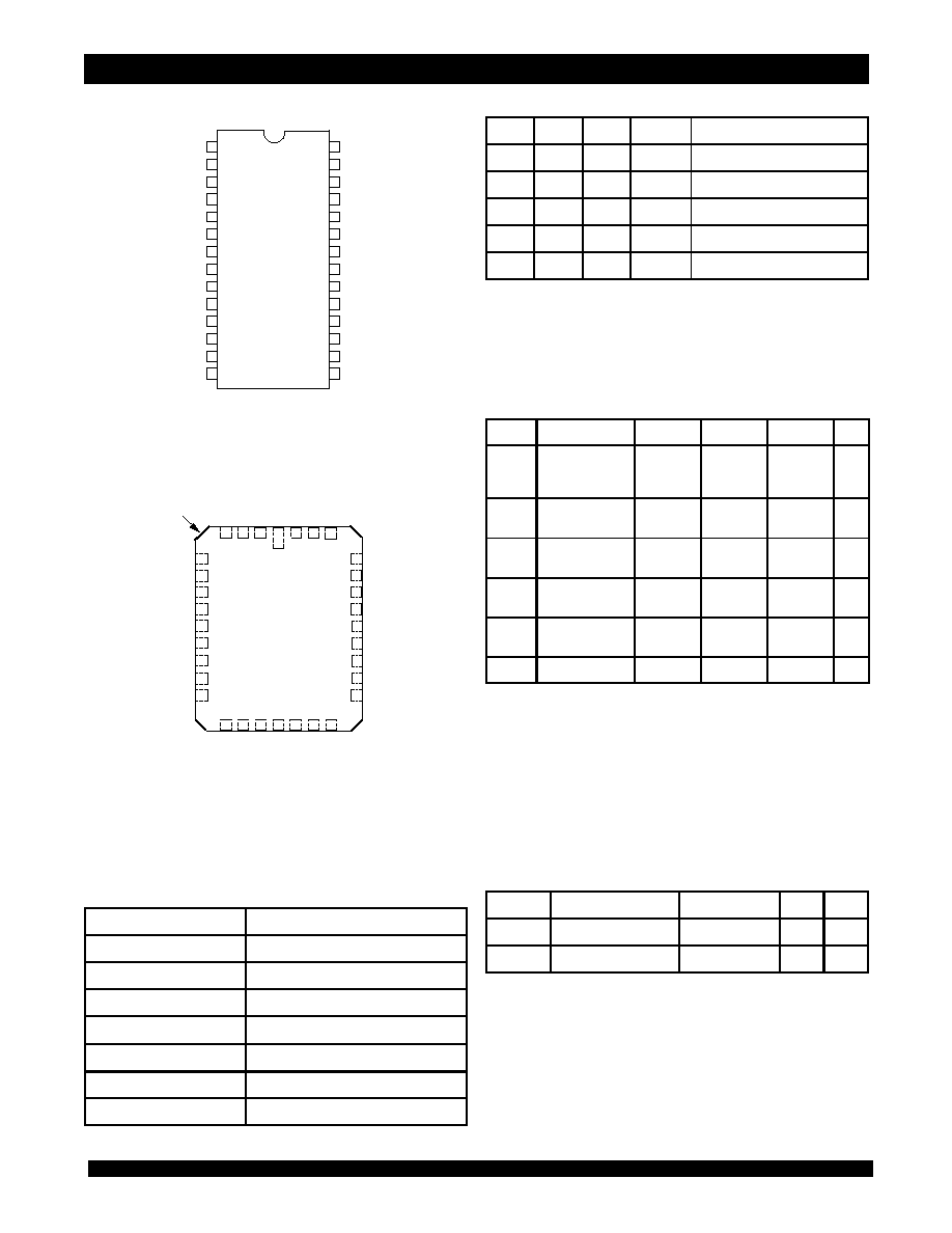
Available in standard 28-pin (300 or 600 mil) ceramic DIP,
28-pin (600 mil) plastic DIP, 28-pin (300 mil) SOJ and
32-pin LCC
x
x
x
x
x
Military product compliant to MIL-STD-883, Class B
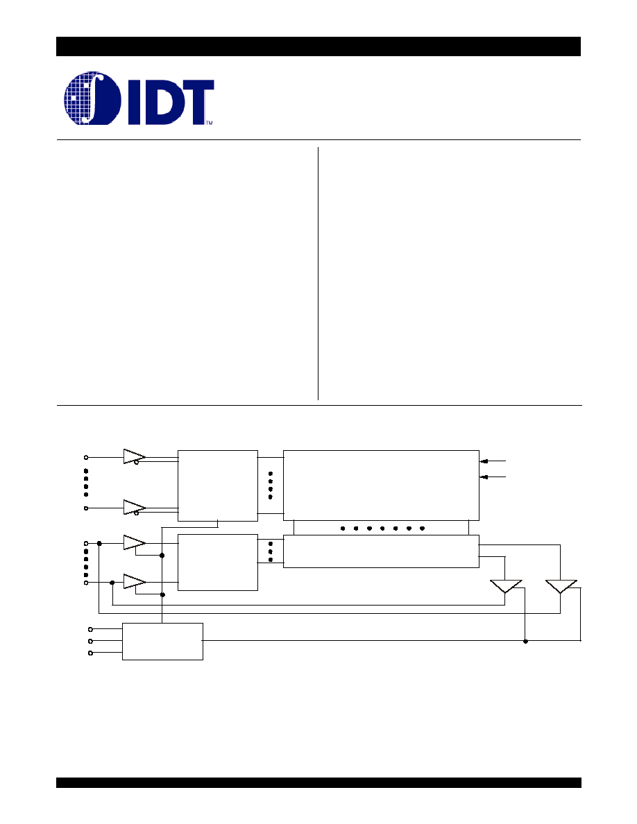
Functional Block Diagram
Description
The IDT 71256 is a 262,144-bit high-speed static RAM organized as
32K x 8. It is fabricated using IDT's high-performance, high-reliability
CMOS technology.
Address access times as fast as 20ns are available with power
consumption of only 350mW (typ.). The circuit also offers a reduced power
standby mode. When
CS goes HIGH, the circuit will automatically go to and
remain in, a low-power standby mode as long as
CS remains HIGH. In
the full standby mode, the low-power device consumes less than 15
µ
W,
typically. This capability provides significant system level power and
cooling savings. The low-power (L) version also offers a battery backup
data retention capability where the circuit typically consumes only 5
µ
W
when operating off a 2V battery.
The IDT71256 is packaged in a 28-pin (300 or 600 mil) ceramic DIP,
a 28-pin 300 mil SOJ, a 28-pin (600 mil) plastic DIP, and a 32-pin LCC
providing high board level packing densities.
The IDT71256 military RAM is manufactured in compliance with the
latest revision of MIL-STD-883, Class B, making it ideally suited to military
temperature applications demanding the highest level of performance and
reliability.
CMOS Static RAM
256K (32K x 8-Bit)
IDT71256S
IDT71256L
A
0
ADDRESS
DECODER
262,144 BIT
MEMORY ARRAY
I/O CONTROL
2946 drw 01
INPUT
DATA
CIRCUIT
WE
CS
V
CC
GND
A
14
I/O
0
I/O
7
CONTROL
CIRCUIT
OE
,
2
IDT71256S/L
CMOS Static RAM 256K (32K x 8-Bit) Military, Commercial, and Industrial Temperature Ranges
Absolute Maximum Ratings
(1)
Pin Configurations
DIP/SOJ
Top View
Truth Table
(1)
32-Pin LCC
Top View
2946 drw 02
5
6
7
8
9
10
11
12
GND
1
2
3
4
24
23
22
21
20
19
18
17
D28-3
P28-1
D28-1
SO28-5
13
14
28
27
26
25
A
7
A
6
A
5
A
4
A
3
A
2
A
1
A
0
I/O
0
I/O
1
I/O
2
V
CC
A
14
WE
A
13
A
8
A
10
A
11
OE
A
12
CS
I/O
7
I/O
6
I/O
5
I/O
4
I/O
3
A
9
16
15
5
6
7
8
9
L32-1
20
19
18
17
10
11
12
13
1
V
16
15
2946 drw 03
14
4
A
3
A
1
,
1
INDEX
2
21
22
23
24
25
26
27
28
29
32 31 30
A
6
A
5
A
4
A
3
A
2
A
1
A
0
NC
I/O
0
A
8
A
9
A
11
NC
OE
A
10
CS
I/O
7
I/O
8
A
7
A
12
A
14
N
C
V
C
C
W
E
A
13
I/
O
1
I/
O
2
G
N
D
N
C
I/
O
3
I/
O
4
I/
O
5
,
Pin Descriptions
Name
Description
A
0
- A
14
Address Inputs
I/O
0
- I/O
7
Data Input/Output
CS
Chip Select
WE
Write Enable
OE
Output Enable
GND
Ground
V
CC
Power
2946 tbl 01
Capacitance
(T
A
= +25∞C, f = 1.0MHz)
NOTE:
1. This parameter is determined by device characterization, but is not production
tested.
NOTE:
1. H = V
IH
, L = V
IL
, X = Don't care.
WE
CS
OE
I/O
Function
X
H
X
High-Z
Standby (I
SB
)
X
V
HC
X
High-Z
Standby (I
SB1
)
H
L
H
High-Z
Output Disabled
H
L
L
D
OUT
Read Data
L
L
X
D
IN
Write Data
2946 tbl 02
NOTE:
1. Stresses greater than those listed under ABSOLUTE MAXIMUM RATINGS
may cause permanent damage to the device. This is a stress rating only and
functional operation of the device at these or any other conditions above those
indicated in the operational sections of this specification is not implied. Exposure
to absolute maximum rating conditions for extended periods may affect
reliability.
Symbol
Rating
Com'l.
Ind.
Mil.
Unit
V
TERM
Terminal Voltage
with Respect
to GND
-0.5 to +7.0 -0.5 to +7.0 -0.5 to +7.0
V
T
A
Operating
Temperature
0 to +70
-40 to +85
-55 to +125
o
C
T
BIAS
Temperature
Under Bias
-55 to +125 -55 to +125 -65 to +135
o
C
T
STG
Storage
Temperature
-55 to +125 -55 to +125 -65 to +150
o
C
P
T
Power
Dissipation
1.0
1.0
1.0
W
I
OUT
DC Output Current
50
50
50
mA
2946 tbl 03
Symbol
Parameter
(1)
Conditions
Max.
Unit
C
IN
Input Capacitance
V
IN
= 0V
11
pF
C
I/O
I/O Capacitance
V
OUT
= 0V
11
pF
2946 tbl 04
6.42
IDT71256S/L
CMOS Static RAM 256K (32K x 8-Bit) Military, Commercial, and Industrial Temperature Ranges
3
Recommended Operating
Temperature and Supply Voltage
Recommended DC Operating
Conditions
NOTE:
1. V
IL
(min.) = ≠3.0V for pulse width less than 20ns, once per cycle.
Grade
Temperature
GND
Vcc
Military
-55
O
C to +125
O
C
0V
5V ± 10%
Industrial
-40
O
C to +85
O
C
0V
5V ± 10%
Commercial
0
O
C to +70
O
C
0V
5V ± 10%
2946 tbl 05
Symbol
Parameter
Min.
Typ.
Max.
Unit
V
CC
Supply Voltage
4.5
5.0
5.5
V
GND
Ground
0
0
0
V
V
IH
Input High Voltage
2.2
____
6.0
V
V
IL
Input Low Voltage
-0.5
(1)
____
0.8
V
2946 tbl 06
DC Electrical Characteristics
(1,2)
(V
CC
= 5.0V ± 10%, V
LC
= 0.2V, V
HC
= V
CC
- 0.2V)
71256S/L20
71256S/L25
71256S/L35
71256S/L45
Symbol
Parameter
Power
Com'l.
Mil.
Com'l
& Ind
Mil.
Com'l.
& Ind
Mil.
Com'l.
Mil.
Unit
I
CC
Dynamic Operating Current
CS < V
IL
, Outputs Open
V
CC
= Max., f
MAX
(2)
S
____
____
____
150
____
140
____
135
mA
L
135
____
115
130
105
120
____
115
I
SB
Standby Power Supply Current
(TTL Level),
CS > V
IH
, V
CC
= Max.,
Outputs Open, f = f
MAX
(2)
S
____
____
____
20
____
20
____
20
mA
L
3
____
3
3
3
3
____
3
I
SB1
Full Standby Power Supply Current
(CMOS Level),
CS > V
HC
,
V
CC
= Max., f = 0
S
____
____
____
20
____
20
____
20
mA
L
0.4
____
0.4
1.5
0.4
1.5
____
1.5
2946 tbl 07
71256S/L55
71256S/L70
71256S/L85
71256S/L100
Symbol
Parameter
Power
Mil.
Mil.
Mil.
Mil.
Unit
I
CC
Dynamic Operating Current
CS < V
IL
, Outputs Open
V
CC
= Max., f
MAX
(2)
S
135
135
135
135
mA
L
115
115
115
115
I
SB
Standby Power Supply Current
(TTL Level),
CS > V
IH
, V
CC
= Max.,
Outputs Open, f = f
MAX
(2)
S
20
20
20
20
mA
L
3
3
3
3
I
SB1
Full Standby Power Supply Current
(CMOS Level),
CS > V
HC
,
V
CC
= Max., f = 0
S
20
20
20
20
mA
L
1.5
1.5
1.5
1.5
2946 tbl 08
NOTES:
1. All values are maximum guaranteed values.
2. f
MAX
= 1/t
RC
, all address inputs are cycling at f
MAX
; f = 0 means no address pins are cycling.
4
IDT71256S/L
CMOS Static RAM 256K (32K x 8-Bit) Military, Commercial, and Industrial Temperature Ranges
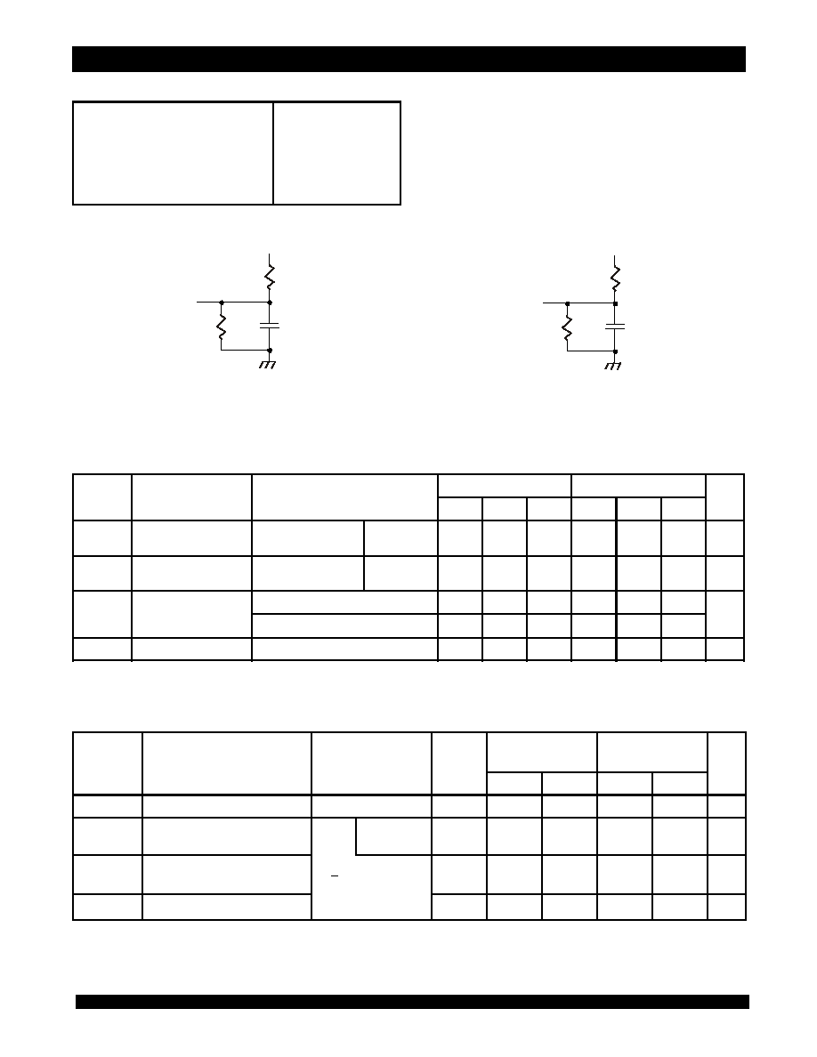
AC Test Conditions
*Includes scope and jig capacitances
Figure 2. AC Test Load
(for t
CLZ
, t
OLZ
, t
CHZ,
t
OHZ
, t
OW
, and t
WHZ
)
Figure 1. AC Test Load
Input Pulse Levels
Input Rise/Fall Times
Input Timing Reference Levels
Output Reference Levels
AC Test Load
GND to 3.0V
5ns
1.5V
1.5V
See Figures 1 and 2
2946 tbl 09
2946 drw 04
480
255
30pF*
DATA
OUT
5V
,
2946 drw 05
480
255
5pF*
DATA
OUT
5V
,
DC Electrical Characteristics
(V
CC
= 5.0V ± 10%)
Data Retention Characteristics Over All Temperature Ranges
(L Version Only) (V
LC
= 0.2V, V
HC
= V
CC
- 0.2V)
NOTES:
1. T
A
= +25∞C.
2. t
RC
= Read Cycle Time.
3. This parameter is guaranteed by device characterization, but is not production tested.
Symbol
Parameter
Test Conditions
IDT71256S
IDT71256L
Unit
Min.
Typ.
Max.
Min.
Typ.
Max.
|I
LI
|
Input Leakage Current
V
CC
= Max.,
V
IN
=
GND to V
CC
MIL.
COM"L & IND.
____
____
____
____
10
5
____
____
____
____
5
2
µ A
|I
LO
|
Output Leakage Current
V
CC
= Max.,
CS = V
IH
,
V
OUT
= GND to V
CC
MIL.
COM"L & IND.
____
____
____
____
10
5
____
____
____
____
5
2
µ A
V
OL
Output Low Voltage
I
OL
= 8mA, V
CC
= Min.
____
____
0.4
____
____
0.4
V
I
OL
= 10mA, V
CC
= Min.
____
____
0.5
____
____
0.5
V
OH
Output High Voltage
I
OH
= -4mA, V
CC
= Min.
2.4
____
____
2.4
____
____
V
2946 tbl 10
Typ.
(1)
V
CC
@
Max.
V
CC
@
Symbol
Parameter
Test Condition
Min.
2.0V
3.0V
2.0V
3.0V
Unit
V
DR
V
CC
for Data Retention
____
2.0
____
____
____
____
V
I
CCDR
Data Retention Current
MIL.
COM'L. & IND.
____
____
____
____
____
____
500
120
800
200
µ
A
t
CDR
Chip Deselect to Data
Retention Time
CS > V
HC
0
____
____
____
____
ns
t
R
(3)
Operation Recovery Time
t
RC
(2)
____
____
____
____
ns
2946 tbl 11
6.42
IDT71256S/L
CMOS Static RAM 256K (32K x 8-Bit) Military, Commercial, and Industrial Temperature Ranges
5
AC Electrical Characteristics
(V
CC
= 5.0V ± 10%, All Temperature Ranges)
Low V
CC
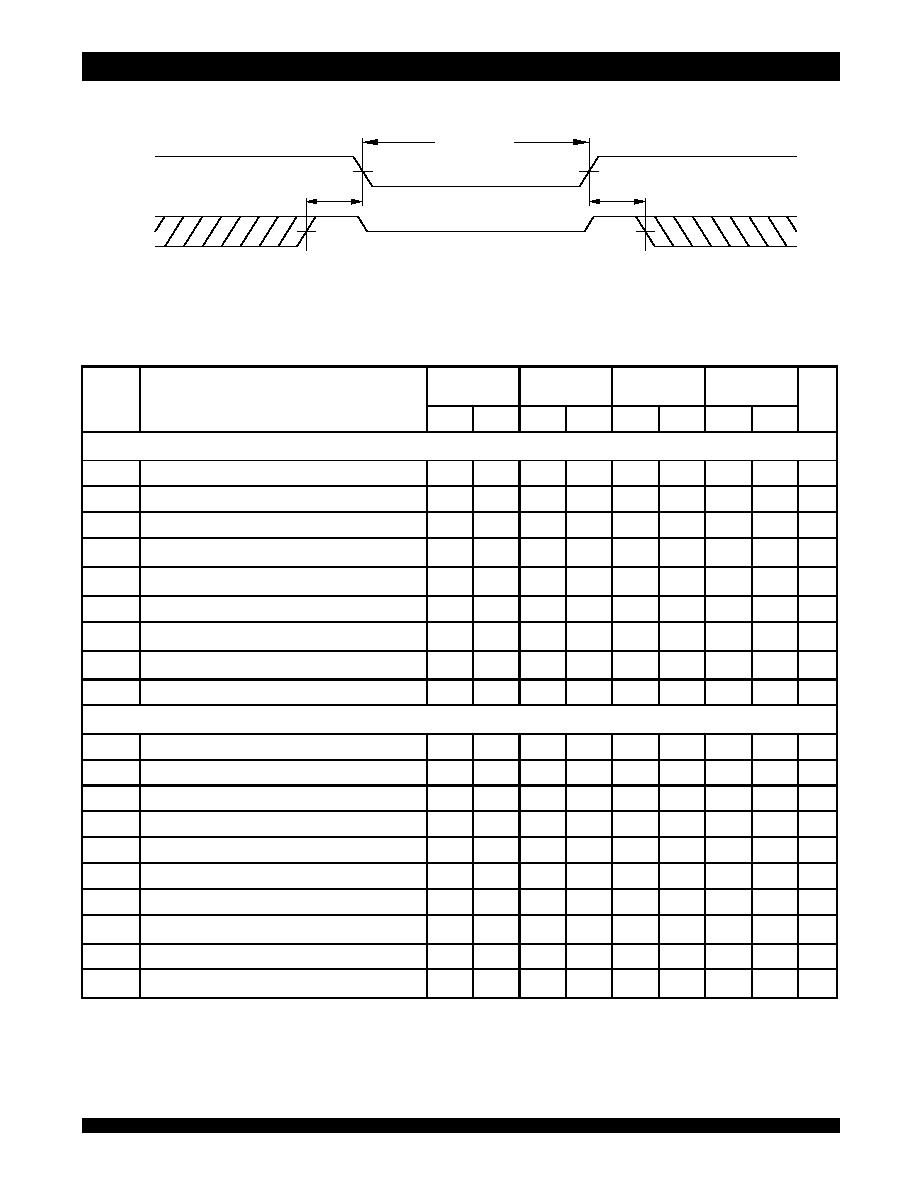
Data Retention Waveform
2946 drw 06
DATA
RETENTION
MODE
4.5V
4.5V
V
DR
2V
V
IH
V
IH
t
R
t
CDR
V
CC
CS
V
DR
NOTES:
1. 0∞ to +70∞C temperature range only.
2. This parameter is guaranteed by device characterization, but is not production tested.
3. ≠55∞C to +125∞C temperature range only.
Symbol
Parameter
71256L20
(1)
71256S25
71256L25
71256S35
71256L35
71256S45
(3)
71256L45
(3)
Unit
Min.
Max.
Min.
Max.
Min.
Max.
Min.
Max.
Read Cycle
t
RC
Read Cycle Time
20
____
25
____
35
____
45
____
ns
t
AA
Address Access Time
____
20
____
25
____
35
____
45
ns
t
ACS
Chip Select Access Time
____
20
____
25
____
35
____
45
ns
t
CLZ
(2)
Chip Select to Output in Low-Z
5
____
5
____
5
____
5
____
ns
t
CHZ
(2)
Chip Desele ct to Output in High-Z
____
10
____
11
____
15
____
20
ns
t
OE
Output Enable to Output Valid
____
10
____
11
____
15
____
20
ns
t
OLZ
(2)
Output Enab le to Output in Low-Z
2
____
2
____
2
____
0
____
ns
t
OHZ
(2)
Output Disab le to Output in High-Z
2
8
2
10
2
15
____
20
ns
t
OH
Output Hold from Address Change
5
____
5
____
5
____
5
____
ns
Write Cycle
t
WC
Write Cycle Time
20
____
25
____
35
____
45
____
ns
t
CW
Chip Select to End-of-Write
15
____
20
____
30
____
40
____
ns
t
AW
Address Valid to End-of-Write
15
____
20
____
30
____
40
____
ns
t
AS
Address Set-up Time
0
____
0
____
0
____
0
____
ns
t
WP
Write Pulse Width
15
____
20
____
30
____
35
____
ns
t
WR
Write Recovery Time
0
____
0
____
0
____
0
____
ns
t
DW
Data to Write Time Overlap
11
____
13
____
15
____
20
____
ns
t
WHZ
(2)
Write Enab le to Output in High-Z
____
10
____
11
____
15
____
20
ns
t
DH
Data Hold from Write Time
0
____
0
____
0
____
0
____
ns
t
OW
(2)
Output Active from End-of-Write
5
____
5
____
5
____
5
____
ns
2946 tbl 12