 | –≠–ª–µ–∫—Ç—Ä–æ–Ω–Ω—ã–π –∫–æ–º–ø–æ–Ω–µ–Ω—Ç: 7164L | –°–∫–∞—á–∞—Ç—å:  PDF PDF  ZIP ZIP |
DECEMBER 2001
DSC-2967/11
1
©2000 Integrated Device Technology, Inc.
Features
x
x
x
x
x
High-speed address/chip select access time
≠ Military: 20/25/35/45/55/70/85/100ns (max.)
≠ Industrial: 25/35ns (max.)
≠ Commercial: 15/20/25/35ns (max.)
x
x
x
x
x
Low power consumption
x
x
x
x
x
Battery backup operation ≠ 2V data retention voltage
(L Version only)
x
x
x
x
x
Produced with advanced CMOS high-performance
technology
x
x
x
x
x
Inputs and outputs directly TTL-compatible
x
x
x
x
x
Three-state outputs
x
x
x
x
x
Available in 28-pin DIP, CERDIP and SOJ
x
x
x
x
x
Military product compliant to MIL-STD-883, Class B
Description
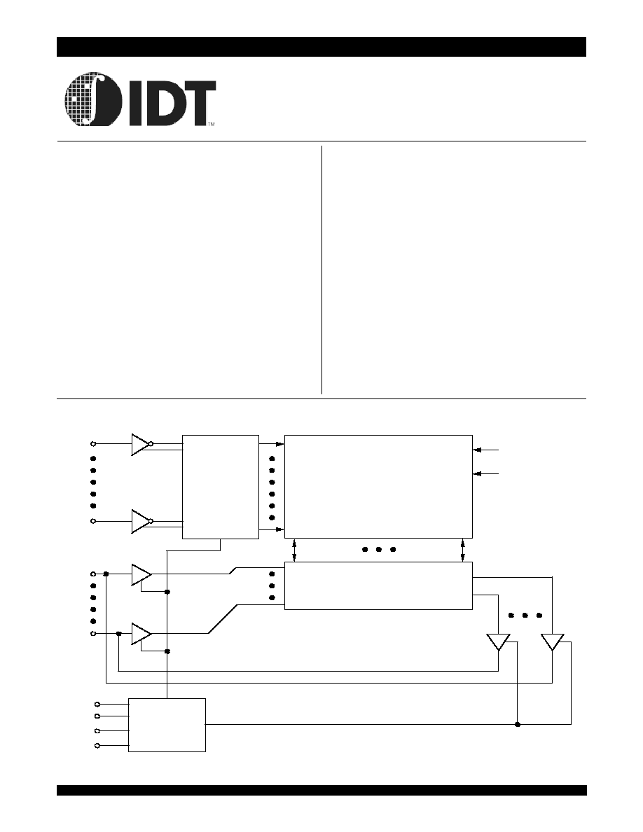
The IDT7164 is a 65,536 bit high-speed static RAM organized as 8K
x 8. It is fabricated using IDT's high-performance, high-reliability CMOS
technology.
Address access times as fast as 15ns are available and the circuit
offers a reduced power standby mode. When
CS
1
goes HIGH or CS
2
goes LOW, the circuit will automatically go to, and remain in, a low-
power stand by mode. The low-power (L) version also offers a battery
backup data retention capability at power supply levels as low as 2V.
All inputs and outputs of the IDT7164 are TTL-compatible and
operation is from a single 5V supply, simplifying system designs. Fully
static asynchronous circuitry is used, requiring no clocks or refreshing
for operation.
The IDT7164 is packaged in a 28-pin 300 mil DIP and SOJ and a 28-
pin 600 mil CERDIP.
Military grade product is manufactured in compliance with the latest
revision of MIL-STD-883, Class B, making it ideally suited to military
temperature applications demanding the highest level of performance
and reliability.
Functional Block Diagram
ADDRESS
DECODER
65,536 BIT
MEMORY ARRAY
I/O CONTROL
2967 drw 01
WE
CS
V
CC
GND
I/O
0
I/O
7
CONTROL
LOGIC
OE
2
CS
1
A
0
A
12
0
7
IDT7164S
IDT7164L
CMOS Static RAM
64K (8K x 8-Bit)
2
IDT7164S/L
CMOS Static RAM 64K (8K x 8-Bit) Military, Commercial, and Industrial Temperature Ranges
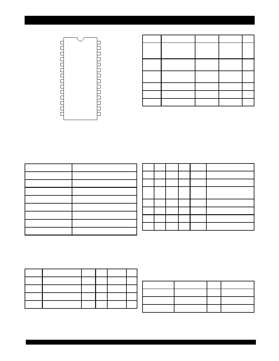
Pin Configurations
Pin Descriptions
Absolute Maximum Ratings
(1)
DIP/SOJ
Top View
Truth Table
(1,2,3)
Recommended Operating
Temperature and Supply Voltage
Recommended DC Operating
Conditions
2967 drw 02
5
6
7
8
9
10
11
12
A
12
1
2
3
4
24
23
22
21
20
19
18
17
D28-1
D28-3
P28-1
P28-2
SO28-5
13
14
28
27
26
25
A
7
A
6
A
5
A
4
A
3
A
2
A
1
A
0
I/O
0
I/O
1
V
CC
WE
A
8
A
9
A
11
OE
A
10
CS
1
I/O
7
16
15
I/O
2
GND
I/O
6
I/O
5
I/O
4
I/O
3
NC
CS
2
,
Name
Description
A
0
- A
12
Address
I/O
0
- I/O
7
Data Input/Output
CS
1
Chip Select
CS
2
Chip Select
WE
Write Enable
OE
Output Enable
GND
Ground
V
CC
Power
2967 tbl 01
NOTES:
1. Stresses greater than those listed under ABSOLUTE MAXIMUM RATINGS may
cause permanent damage to the device. This is a stress rating only and functional
operation of the device at these or any other conditions above those indicated in the
operational sections of this specification is not implied. Exposure to absolute
maximum rating conditions for extended periods may affect reliability.
2. V
TERM
must not exceed V
CC
+ 0.5V.
Symbol
Rating
Com'l.
Mil.
Unit
V
TERM
(2)
Terminal Voltage
with Respect
to GND
-0.5 to +7.0
-0.5 to +7.0
V
T
A
Operating
Temperature
0 to +70
-55 to +125
o
C
T
BIAS
Temperature
Under Bias
-55 to +125
-65 to +135
o
C
T
STG
Storage Temperature
-55 to +125
-65 to +150
o
C
P
T
Power Dissipation
1.0
1.0
W
I
OUT
DC Output Current
50
50
mA
2967 tbl 02
NOTES:
1. CS
2
will power-down
CS
1
, but
CS
1
will not power-down CS
2
.
2. H = V
IH
, L = V
IL
, X = don't care.
3. V
LC
= 0.2V, V
HC
= V
CC
- 0.2V
WE
CS
1
CS
2
OE
I/O
Function
X
H
X
X
High-Z
Deselected - Standby (I
SB
)
X
X
L
X
High-Z
Deselected - Standby (I
SB
)
X
V
HC
V
HC
or
V
LC
X
High-Z
Deselected - Standby (I
SB1
)
X
X
V
LC
X
High-Z
Deselected - Standby (I
SB1
)
H
L
H
H
High-Z
Output Disabled
H
L
H
L
DATA
OUT
Read Data
L
L
H
X
DATA
IN
Write Data
2967 tbl 03
Grade
Temperature
GND
Vcc
Military
-55
O
C to +125
O
C
0V
5V ± 10%
Industrial
-40
O
C to +85
O
C
0V
5V ± 10%
Commercial
0
O
C to +70
O
C
0V
5V ± 10%
2967 tbl 04
NOTE:
1. V
IL
(min.) = ≠1.5V for pulse width less than 10ns, once per cycle.
Symbol
Parameter
Min.
Typ.
Max.
Unit
V
CC
Supply Voltage
4.5
5.0
5.5
V
GND
Ground
0
0
0
V
V
IH
Input HIGH Voltage
2.2
____
V
CC
+ 0.5
V
V
IL
Input LOW Voltage
-0.5
(1)
____
0.8
V
2967 tbl 05

6.42
IDT7164S/L
CMOS Static RAM 64K (8K x 8-Bit) Military, Commercial, and Industrial Temperature Ranges
3
DC Electrical Characteristics
(1)
(V
CC
= 5.0V ± 10%, V
LC
= 0.2V, V
HC
= V
CC
- 0.2V)
Capacitance
(T
A
= +25∞C, f = 1.0MHz)
NOTE:
1. This parameter is determined by device characterization, but is not production
tested.
Symbol
Parameter
(1)
Conditions
Max.
Unit
C
IN
Input Capacitance
V
IN
= 0V
8
pF
C
I/O
I/O Capacitance
V
OUT
= 0V
8
pF
2967 tbl 06
Symbol
Parameter
Power
7164S15
7164L15
7164S20
7164L20
7164S25
7164L25
Unit
Com'l.
Com'l.
Mil.
Com'l.
Ind.
Mil.
I
CC1
Operating Power Supply Current
CS
1
= V
IL
, CS
2
= V
IH
, Outputs Open
V
CC
= Max., f
=
0
(2)
S
110
100
110
90
90
110
mA
L
100
90
100
80
80
100
I
CC2
Dynamic Operating Current
CS
1
= V
IL
, CS
2
= V
IH
, Outputs Open
V
CC
= Max., f = f
MAX
(2)
S
180
170
180
170
170
180
mA
L
150
150
160
150
150
160
I
SB
Standby Power Supply Current
(TTL Level),
CS
1
> V
IH
, CS
2
< V
IL
,
Outputs Open, V
CC
= Max., f = f
MAX
(2)
S
20
20
20
20
20
20
mA
L
3
3
5
3
3
5
I
SB1
Full Standby Power Supply Current
(CMOS Level), f = 0
(2)
, V
CC
= Max.
1.
CS
1
> V
HC
and CS
2
> V
HC
, or
2. CS
2
< V
LC
S
15
15
20
15
15
20
mA
L
0.2
0.2
1
0.2
0.2
1
2967 tbl 07
NOTES:
1. All values are maximum guaranteed values.
2. f
MAX
= 1/t
RC
(all address inputs are cycling at f
MAX
); f = 0 means no address input lines are changing.
Symbol
Parameter
Power
7164S35
7164L35
7164S45
7164L45
7164S55
7164L55
7164S70
7164L70
7164S85/100
7164L85/100
Unit
Com'l.
Ind.
Mil.
Mil.
Mil.
Mil.
Mil.
I
CC1
Operating Power Supply Current
CS
1
= V
IL
, CS
2
= V
IH
, Outputs Open
V
CC
= Max., f
=
0
(2)
S
90
90
100
100
100
100
100
mA
L
80
80
90
90
90
90
90
I
CC2
Dynamic Operating Current
CS
1
= V
IL
, CS
2
= V
IH
, Outputs Open
V
CC
= Max., f = f
MAX
(2)
S
150
150
160
160
160
160
160
mA
L
130
130
140
130
125
120
120
I
SB
Standby Power Supply Current
(TTL Level),
CS
1
> V
IH
, CS
2
< V
IL
,
Outputs Open, V
CC
= Max., f = f
MAX
(2)
S
20
20
20
20
20
20
20
mA
L
3
3
5
5
5
5
5
I
SB1
Full Standby Power Supply Current
(CMOS Level), f = 0
(2)
, V
CC
= Max.
1.
CS
1
> V
HC
and CS
2
> V
HC
, or
2. CS
2
< V
LC
S
15
15
20
20
20
20
20
mA
L
0.2
0.2
1
1
1
1
1
2967 tbl 08
4
IDT7164S/L
CMOS Static RAM 64K (8K x 8-Bit) Military, Commercial, and Industrial Temperature Ranges
DC Electrical Characteristics
(V
CC
= 5.0V ± 10%)
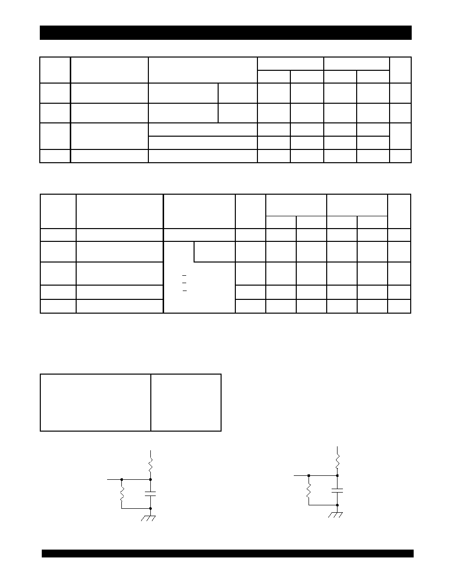
AC Test Conditions
*Includes scope and jig capacitances
Figure 2. AC Test Load
(for t
CLZ1,
t
CLZ2
, t
OLZ
, t
CHZ1,
t
CHZ2
, t
OHZ
, t
OW
, and t
WHZ
)
Figure 1. AC Test Load
Data Retention Characteristics Over All Temperature Ranges
(L Version Only) (V
LC
= 0.2V, V
HC
= V
CC
- 0.2V)
2967 drw 03
480
30pF*
255
DATA
OUT
5V
,
2967 drw 04
480
5pF*
255
DATA
OUT
5V
,
Symbol
Parameter
Test Conditions
IDT7164S
IDT7164L
Unit
Min.
Max.
Min.
Max.
|I
LI
|
Input Leakage Current
V
CC
= Max.,
V
IN
=
GND to V
CC
MIL.
COM'L. & IND
____
____
10
5
____
____
5
2
µA
|I
LO
|
Output Leakage Current
V
CC
= Max.,
CS
1
= V
IH
,
V
OUT
= GND to V
CC
MIL.
COM'L. & IND
____
____
10
5
____
____
5
2
µA
V
OL
Output Low Voltage
I
OL
= 8mA, V
CC
= Min.
____
0.4
____
0.4
V
I
OL
= 10mA, V
CC
= Min.
____
0.5
____
0.5
V
OH
Output High Voltage
I
OH
= -4mA, V
CC
= Min.
2.4
____
2.4
____
V
2967 tbl 09
NOTES:
1. T
A
= +25∞C.
2. t
RC
= Read Cycle Time.
3. This parameter is guaranteed by device characterization, but is not production tested.
Typ.
(1)
V
CC
@
Max.
V
CC
@
Symbol
Parameter
Test Condition
Min.
2.0V
3.0V
2.0V
3.0V
Unit
V
DR
V
CC
for Data Retention
____
2.0
____
____
____
____
V
I
CCDR
Data Retention Current
MIL.
COM'L. & IND
____
____
10
10
15
15
200
60
300
90
µ
A
t
CDR
(3)
Chip Deselect to Data
Retention Time
1.
CS
1
> V
HC
CS
2
> V
HC
, or
2. CS
2
< V
LC
0
____
____
____
____
ns
t
R
(3)
Operation Recovery Time
t
RC
(2)
____
____
____
____
ns
I
I
LI
I
(3)
Input Leakage Current
____
____
____
2
2
µ
A
2967 tbl 10
Input Pulse Levels
Input Rise/Fall Times
Input Timing Reference Levels
Output Reference Levels
AC Test Load
GND to 3.0V
5ns
1.5V
1.5V
See Figures 1 and 2
2967 tbl 11

6.42
IDT7164S/L
CMOS Static RAM 64K (8K x 8-Bit) Military, Commercial, and Industrial Temperature Ranges
5
AC Electrical Characteristics
(V
CC
= 5.0V ± 10%, All Temperature Ranges)
NOTES:
1. 0∞ to +70∞C temperature range only.
2. 0∞ to +70∞C and ≠55∞C to +125∞C temperature ranges only.
3. Both chip selects must be active for the device to be selected.
4. This parameter is guaranteed by device characterization, but is not production tested.
Symbol
Parameter
7164S15
(1)
7164L15
(1)
7164S20
(2)
7164L20
(2)
7164S25
7164L25
7164S35
7164L35
Unit
Min.
Max.
Min.
Max.
Min.
Max.
Min.
Max.
Read Cycle
t
RC
Read Cycle Time
15
____
20
____
25
____
35
____
ns
t
AA
Address Access Time
____
15
____
19
____
25
____
35
ns
t
ACS1
(3)
Chip Select-1 Access Time
____
15
____
20
____
25
____
35
ns
t
ACS2
(3)
Chip Select-2 Access Time
____
20
____
25
____
30
____
40
ns
t
CLZ1,2
(4)
Chip Select-1, 2 to Output in Low-Z
5
____
5
____
5
____
5
____
ns
t
OE
Output Enable to Output Valid
____
7
____
8
____
12
____
18
ns
t
OLZ
(4)
Output Enab le to Output in Low-Z
0
____
0
____
0
____
0
____
ns
t
CHZ1,2
(4)
Chip Select-1,2 to Output in High-Z
____
8
____
9
____
13
____
15
ns
t
OHZ
(4)
Output Disab le to Output in High-Z
____
7
____
8
____
10
____
15
ns
t
OH
Output Hold from Address Change
5
____
5
____
5
____
5
____
ns
t
PU
(4)
Chip Sele ct to Power Up Time
0
____
0
____
0
____
0
____
ns
t
PD
(4)
Chip Deselect to Power Down Time
____
15
____
20
____
25
____
35
ns
Write Cycle
t
WC
Write Cycle Time
15
____
20
____
25
____
35
____
ns
t
CW1,2
Chip Select to End-of-Write
14
____
15
____
18
____
25
____
ns
t
AW
Address Valid to End-of-Write
14
____
15
____
18
____
25
____
ns
t
AS
Address Set-up Time
0
____
0
____
0
____
0
____
ns
t
WP
Write Pulse Width
14
____
15
____
21
____
25
____
ns
t
WR1
Write Recovery Time (
CS
1
,
WE)
0
____
0
____
0
____
0
____
ns
t
WR2
Write Recovery Time (CS
2
)
5
____
5
____
5
____
5
____
ns
t
WHZ
(4)
Write Enab le to Output in High-Z
____
6
____
8
____
10
____
14
ns
t
DW
Data to Write Time Overlap
8
____
10
____
13
____
15
____
ns
t
DH1
Data Hold from Write Time (
CS
1
,
WE)
0
____
0
____
0
____
0
____
ns
t
DH2
Data Hold from Write Time (CS
2
)
5
____
5
____
5
____
5
____
ns
t
OW
(4)
Output Active from End-of-Write
4
____
4
____
4
____
4
____
ns
2967 tbl 12