1
©2000 Integrated Device Technology, Inc.
AUGUST 2001
DSC-3729/04
Pin Description
Features
x
x
x
x
x
32K x 32 memory configuration
x
x
x
x
x
Supports high performance system speed:
Commercial and Industrial:
-- 11 11ns Clock-to-Data Access (50MHz)
-- 12 12ns Clock-to-Data Access (50MHz)
x
x
x
x
x
LBO input selects interleaved or linear burst mode
x
x
x
x
x
Self-timed write cycle with global write control (
GW), byte
write enable (
BWE), and byte writes (BWx)
x
x
x
x
x
Power down controlled by ZZ input
x
x
x
x
x
Single 3.3V power supply (+10/-5%)
x
x
x
x
x
Packaged in a JEDEC Standard 100-pin rectangular plastic
thin quad flatpack (TQFP).
Description
The IDT71V433 is a 3.3V high-speed 1,048,576-bit SRAM orga-
nized as 32K x 32 with full support of various processor interfaces
including the PentiumTM and PowerPCTM. The flow-through burst archi-
tecture provides cost-effective 2-1-1-1 performance for processors up to
50 MHz.
32K x 32
3.3V Synchronous SRAM
Flow-Through Outputs
IDT71V433
A
0
≠A
14
Address Inputs
Input
Synchronous
CE
Chip Enable
Input
Synchronous
CS
0
,
CS
1
Chips Selects
Input
Synchronous
OE
Output Enable
Input
Asynchronous
GW
Global Write Enable
Input
Synchronous
BWE
Byte Write Enable
Input
Synchronous
BW
1
≠
BW
4
Individual Byte Write Selects
Input
Synchronous
CLK
Clock Input
Input
N/A
ADV
Burst Address Advance
Input
Synchronous
ADSC
Address Status (Cache Controller)
Input
Synchronous
ADSP
Address Status (Processor)
Input
Synchronous
LBO
Linear / Interleaved Burst Order
Input
DC
ZZ
Sleep Mode
Input
Asynchronous
I/O
0
≠I/O
31
Data Input/Output
I/O
Synchronous
V
DD
, V
DDQ
Co re and I/O Power Supply (3.3V)
Power
N/A
V
SS
, V
SSQ
Array Ground, I/O Ground
Power
N/A
3729 tbl 01
Pentium is a trademark of Intel Corp.
PowerPC is a trademark of International Business Machines, Inc.
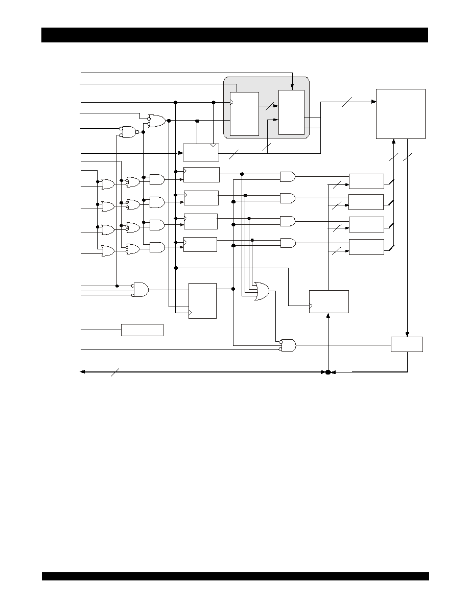
The IDT71V433 SRAM contains write, data-input, address and
control registers. There are no registers in the data output path (flow-
through architecture). Internal logic allows the SRAM to generate a
self-timed write based upon a decision which can be left until the
extreme end of the write cycle.
The burst mode feature offers the highest level of performance to
the system designer, as the IDT71V433 can provide four cycles of data
for a single address presented to the SRAM. An internal burst address
counter accepts the first cycle address from the processor, initiating the
access sequence. The first cycle of output data will flow-through from
the array after a clock-to-data access time delay from the rising clock
edge of the same cycle. If burst mode operation is selected (
ADV=LOW),
the subsequent three cycles of output data will be available to the
user on the next three rising clock edges. The order of these three
addresses will be defined by the internal burst counter and the
LBO
input pin.
The IDT71V433 SRAM utilizes IDT's high-performance 3.3V
CMOS process, and is packaged in a JEDEC Standard 14mm x 20mm
100-pin thin plastic quad flatpack (TQFP).
2
IDT71V433
32K x 32, 3.3V Synchronous SRAM with Flow-Through Outputs Commercial and Industrial Temperature Ranges
Pin Definitions
(1)
Symbol
Pin Function
I/O
Active
Description
A
0
≠A
14
Address Inputs
I
N/A
Synchronous Address inputs. The address register is triggered by a combination
of the rising edge of CLK and
ADSC Low or ADSP Low and CE Low.
ADSC
Address Status
(Cache Controller)
I
LOW
Synchronous Address Status from Cache Controller.
ADSC is an active LOW input
that is used to load the address registers with new addresses.
ADSC is NOT gated
by
CE.
ADSP
Address Status (Processor)
I
LOW
Synchronous Address Status from Processor.
ADSP is an active LOW input that
is used to load the address registers with new addresses.
ADSP is gated by CE.
ADV
Burst Address Advance
I
LOW
Sync hrono us Ad dress Adv ance.
ADV is an active LOW input that is used to
advance the internal burst counter, controlling burst access after the initial address
is loaded. When this input is HIGH the burst counter is not incremented; that is,
there is no address advance.
BWE
Byte Write Enable
I
LOW
Synchronous b yte write enable gates the byte write inputs
BW
1
≠
BW
4
. If
BWE is
LOW at the rising edge of CLK then
BW
X
inputs are passed to the next stage in
the circuit. A byte write can still be blocked if
ADSP is LOW at the rising edge of
CLK. If
ADSP is HIGH and BW
X
is LOW at the rising edge of CLK then data will
be written to the SRAM. If
BWE is HIGH then the byte write inputs are blocked
and only
GW can initiate a write cycle.
BW
1
≠
BW
4
Individual Byte Write
Enables
I
LOW
Synchronous byte write enables.
BW
1
controls I/O(7:0),
BW
2
controls I/O(15:8),
etc. Any active byte write causes all outputs to be disabled.
ADSP LOW disables
all byte writes.
BW
1
≠
BW
4
must meet specified setup and hold times with respect
to CLK.
CE
Chip Enable
I
LOW
Synchronous chip enable.
CE is used with CS
0
and
CS
1
to enable the IDT71V433.
CE also gates ADSP.
CLK
Clock
I
N/A
This is the clock input. All timing references for the device are made with respect
to this input.
CS
0
Chip Select 0
I
HIGH
Synchronous active HIGH chip select. CS
0
is used with
CE and CS
1
to enable the
chip.
CS
1
Chip Select 1
I
LOW
Synchro nous active LOW chip select.
CS
1
is used with
CE and CS
0
to enable the
chip.
GW
Global Write Enable
I
LOW
Synchronous global write enable. This input will write all four 8-bit data bytes when
LOW on the rising edge of CLK.
GW supercedes individual byte write enables.
I/O
0
≠I/O
31
Data Input/Output
I/O
N/A
Synchronous data input/output (I/O) pins. Only the data input path is registered
and triggered by the rising edge of CLK. Outputs are Flow-Through.
LBO
Linear Burst
I
LOW
When
LBO is HIGH the Interleaved Order (Intel) burst sequence is selected. When
LBO is LOW the Linear (PowerPC) burst sequence is selected. LBO has an internal
pull-up resistor.
OE
Output Enable
I
LOW
Asynchronous output e nable. Whe n
OE is HIGH the I/O pins are in a high-
impedence state. When
OE is LOW the data output drivers are enabled if the chip
is also selected.
V
DD
Power Supply
N/A
N/A
3.3V core power supply inputs.
V
DDQ
Power Supply
N/A
N/A
3.3V I/O power supply inputs.
V
SS
Ground
N/A
N/A
Core ground pins.
V
SSQ
Ground
N/A
N/A
I/O ground pins.
NC
No Connect
N/A
N/A
NC pins are not electrically connected to the chip.
ZZ
Sleep Mode
I
HIGH
Asynchronous sleep mode input. ZZ HIGH will gate the CLK internally and power
down the IDT71V433 to its lowe st power consumption level. Data retention is
guaranteed in Sleep Mode. ZZ has an internal pull-down resistor.
3729 tbl 02
NOTE:
1. All synchronous inputs must meet specified setup and hold times with respect to CLK.
6.42
IDT71V433
32K x 32, 3.3V Synchronous SRAM with Flow-Through Outputs Commercial and Industrial Temperature Ranges
3
Functional Block Diagram
A
0
≠A
14
ADDRESS
REGISTER
CLR
A
1
*
A
0
*
15
2
15
A
2
≠A
14
32K x 32
BIT
MEMORY
ARRAY
INTERNAL
ADDRESS
A
0
, A
1
BW
4
BW
3
BW
2
BW
1
Byte 1
Write Register
32
32
ADSP
ADV
CLK
ADSC
CS
0
CS
1
Byte 1
Write Driver
Byte 2
Write Driver
Byte 3
Write Driver
Byte 4
Write Driver
Byte 2
Write Register
Byte 3
Write Register
Byte 4
Write Register
8
8
8
8
GW
CE
BWE
LBO
I/O
0
≠I/O
31
OE
DATA INPUT
REGISTER
32
OUTPUT
BUFFER
Powerdown
ZZ
D
Q
Enable
Register
OE
Burst
Sequence
CE
CLK EN
CLK EN
Q1
Q0
2
Burst
Logic
Binary
Counter
3729 drw 01
.
4
IDT71V433
32K x 32, 3.3V Synchronous SRAM with Flow-Through Outputs Commercial and Industrial Temperature Ranges
Absolute Maximum DC Ratings
(1)
Capacitance
(T
A
= +25∞C, f = 1.0MHz, TQFP package)
NOTES:
1. Stresses greater than those listed under ABSOLUTE MAXIMUM RATINGS may
cause permanent damage to the device. This is a stress rating only and functional
operation of the device at these or any other conditions above those indicated
in the operational sections of this specification is not implied. Exposure to absolute
maximum rating conditions for extended periods may affect reliability.
2. V
DD
, V
DDQ
and input terminals only.
3. I/O terminals.
Symbol
Rating
Value
Unit
V
TERM
(2)
Terminal Voltage with
Respect to GND
≠0.5 to +4.6
V
V
TERM
(3)
Terminal Voltage with
Respect to GND
≠0.5 to V
DD
+0.5
V
T
A
Operating Temperature
0 to +70
o
C
T
BIAS
Temperature Under Bias
≠55 to +125
o
C
T
STG
Storage Temperature
≠55 to +125
o
C
P
T
Power Dissipation
1.2
W
I
OUT
DC Output Current
50
mA
3729 tbl 05
NOTE:
1. This parameter is guaranteed by device characterization, but not production
tested.
Symbol
Parameter
(1)
Conditions
Max.
Unit
C
IN
Input Capacitance
V
IN
= 3dV
4
pF
C
I/O
I/O Capacitance
V
OUT
= 3dV
8
pF
3729 tbl 06
Recommended DC Operating
Conditions
NOTES:
1. V
IH
and V
IL
as indicated is for both input and I/O pins.
2. V
IH
(max) = 6.0V for pulse width less than t
CYC
/2, once per cycle.
3. V
IL
(min) = ≠1.0V for pulse width less than t
CYC
/2, once per cycle.
Symbol
Parameter
Min.
Typ.
Max.
Unit
V
DD
Core Supply Voltage
3.135
3.3
3.63
V
V
DDQ
I/O Supply Voltage
3.135
3.3
3.63
V
V
SS,
V
SSQ
Ground
0
0
0
V
V
IH
Input High Voltage
2.0
(1)
____
V
DDQ
+0.3
(2)
V
V
IL
Input Low Voltage
≠0.5
(3)
____
0.8
V
3729 tbl 04
Grade
Temperature
V
SS
V
DD
V
DDQ
Commercial
0∞C to +70∞C
0V
3.3V+10/-5% 3.3V+10/-5%
Industrial
≠40∞C to +85∞C
0V
3.3V+10/-5% 3.3V+10/-5%
3729 tbl 03
Recommended Operating
Temperature and Supply Voltage
6.42
IDT71V433
32K x 32, 3.3V Synchronous SRAM with Flow-Through Outputs Commercial and Industrial Temperature Ranges
5
100 99 98 97 96 95 94 93 92 91 90
87 86 85 84 83 82 81
89 88
1
2
3
4
5
6
7
8
9
10
11
12
13
14
15
16
17
18
19
20
21
22
23
24
25
26
27
28
29
30
A
6
A
7
C
E
C
S
0
B
W
4
B
W
3
B
W
2
B
W
1
C
S
1
V
D
D
V
S
S
C
L
K
G
W
B
W
E
O
E
A
D
S
C
A
D
S
P
A
D
V
A
8
A
9
NC
31 32 33 34 35 36 37 38 39 40 41 42 43 44 45 46 47 48 49 50
N
C
N
C
N
C
N
C
N
C
LB
O
A
14
A
13
A
12
A
11
A
10
V
D
D
V
S
S
A
0
A
1
A
2
A
3
A
4
A
5
I/O
31
I/O
30
V
DDQ
V
SSQ
I/O
29
I/O
28
I/O
27
I/O
26
V
SSQ
V
DDQ
I/O
25
I/O
24
V
SS
V
DD
I/O
23
I/O
22
V
DDQ
V
SSQ
I/O
21
I/O
20
I/O
19
I/O
18
V
SSQ
V
DDQ
I/O
17
I/O
16
80
79
78
77
76
75
74
73
72
71
70
69
68
67
66
65
64
63
62
61
60
59
58
57
56
55
54
53
52
51
I/O
14
V
DDQ
V
SSQ
I/O
13
I/O
12
I/O
11
I/O
10
V
SSQ
V
DDQ
I/O
9
I/O
8
V
SS
NC
V
DD
ZZ
(2)
I/O
7
I/O
6
V
DDQ
V
SSQ
I/O
5
I/O
4
I/O
3
I/O
2
V
SSQ
V
DDQ
I/O
1
I/O
0
PK100-1
3729 drw 02
V
SS
(1)
I/O
15
NC
NC
NC
NC
N
C
.
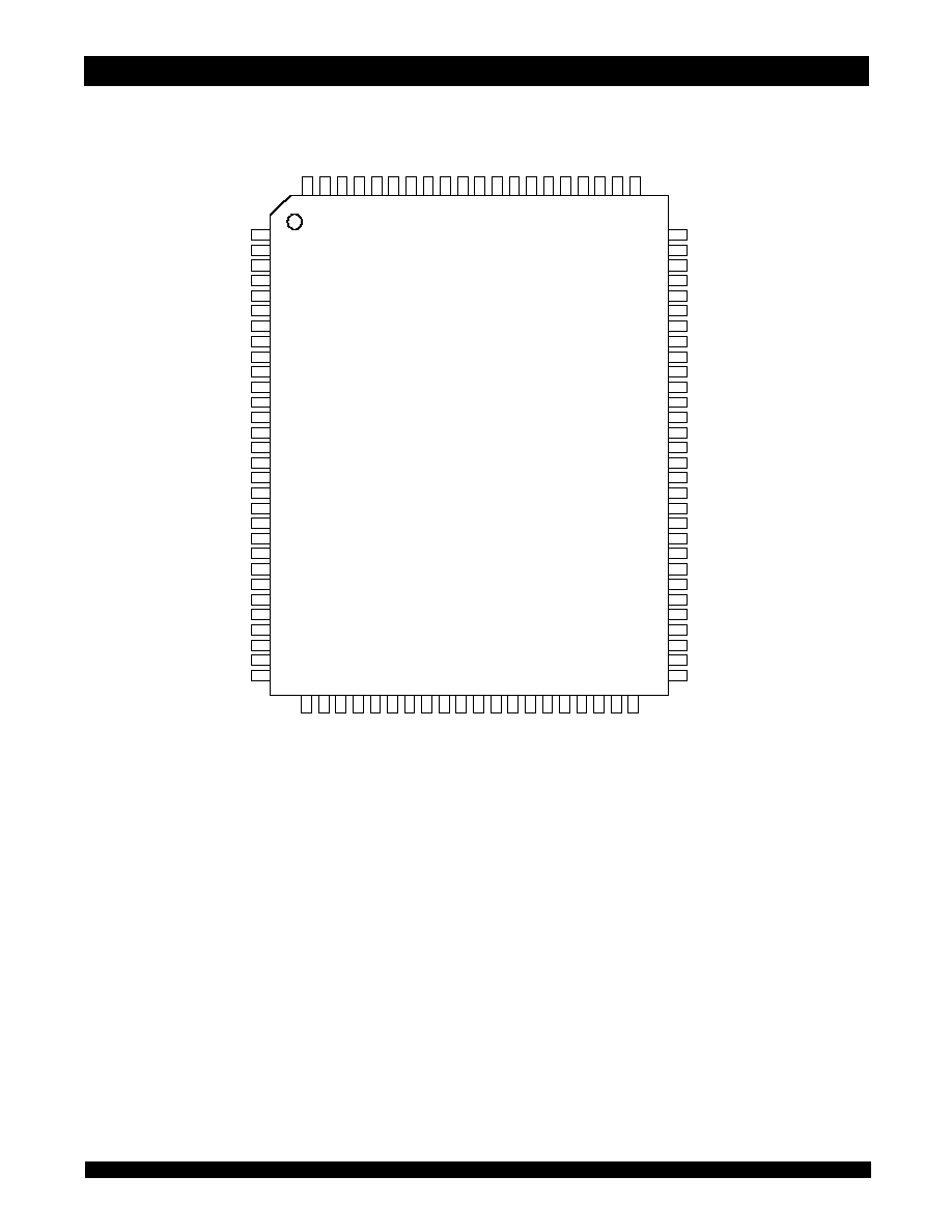
Pin Configuration
Top View TQFP
NOTES
1. Pin 14 does not have to be directly connected to V
SS
as long as the input voltage is
V
IL
.
2. Pin 64 can be left unconnected and the device will always remain in active mode.
6
IDT71V433
32K x 32, 3.3V Synchronous SRAM with Flow-Through Outputs Commercial and Industrial Temperature Ranges
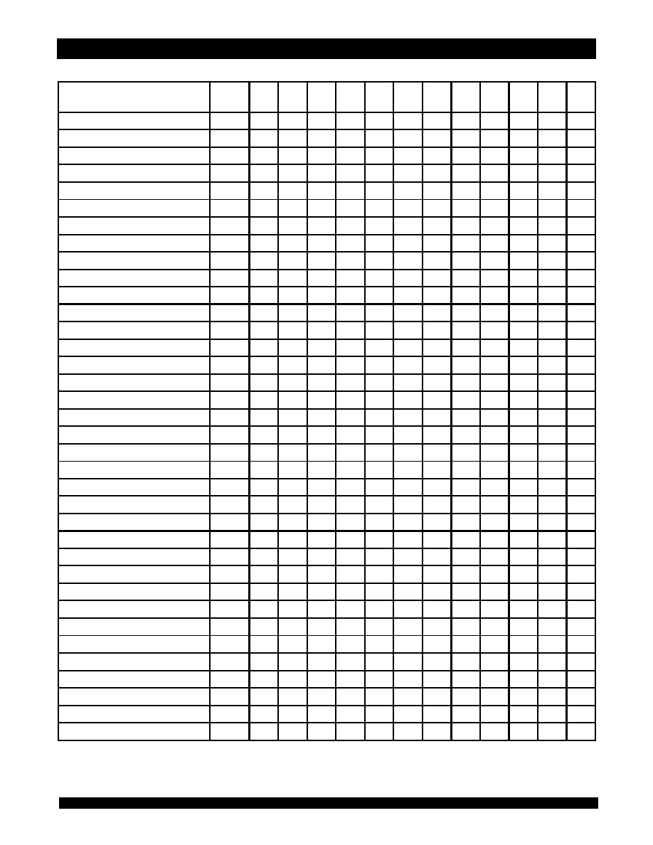
Synchronous Truth Table
(1, 2)
NOTES:
1. L = V
IL
, H = V
IH
, X = Don't Care.
2. ZZ = LOW for this table.
3.
OE is an asynchronous input.
Operation
Address
Used
CE
CS
0
CS
1
ADSP ADSC
ADV
GW
BWE
BW
X
OE
(3)
CLK
I/O
Deselected Cycle, Power Down
None
H
X
X
X
L
X
X
X
X
X
Hi-Z
Deselected Cycle, Power Down
None
L
X
H
L
X
X
X
X
X
X
Hi-Z
Deselected Cycle, Power Down
None
L
L
X
L
X
X
X
X
X
X
Hi-Z
Deselected Cycle, Power Down
None
L
X
H
X
L
X
X
X
X
X
Hi-Z
Deselected Cycle, Power Down
None
L
L
X
X
L
X
X
X
X
X
Hi-Z
Read Cycle, Begin Burst
External
L
H
L
L
X
X
X
X
X
L
D
OUT
Read Cycle, Begin Burst
External
L
H
L
L
X
X
X
X
X
H
Hi-Z
Read Cycle, Begin Burst
External
L
H
L
H
L
X
H
H
X
L
D
OUT
Read Cycle, Begin Burst
External
L
H
L
H
L
X
H
L
H
L
D
OUT
Read Cycle, Begin Burst
External
L
H
L
H
L
X
H
L
H
H
Hi-Z
Write Cycle, Begin Burst
External
L
H
L
H
L
X
H
L
L
X
D
IN
Write Cycle, Begin Burst
External
L
H
L
H
L
X
L
X
X
X
D
IN
Read Cycle, Continue Burst
Next
X
X
X
H
H
L
H
H
X
L
D
OUT
Read Cycle, Continue Burst
Next
X
X
X
H
H
L
H
H
X
H
Hi-Z
Read Cycle, Continue Burst
Next
X
X
X
H
H
L
H
X
H
L
D
OUT
Read Cycle, Continue Burst
Next
X
X
X
H
H
L
H
X
H
H
Hi-Z
Read Cycle, Continue Burst
Next
H
X
X
X
H
L
H
H
X
L
D
OUT
Read Cycle, Continue Burst
Next
H
X
X
X
H
L
H
H
X
H
Hi-Z
Read Cycle, Continue Burst
Next
H
X
X
X
H
L
H
X
H
L
D
OUT
Read Cycle, Continue Burst
Next
H
X
X
X
H
L
H
X
H
H
Hi-Z
Write Cycle, Continue Burst
Next
X
X
X
H
H
L
H
L
L
X
D
IN
Write Cycle, Continue Burst
Next
X
X
X
H
H
L
L
X
X
X
D
IN
Write Cycle, Continue Burst
Next
H
X
X
X
H
L
H
L
L
X
D
IN
Write Cycle, Continue Burst
Next
H
X
X
X
H
L
L
X
X
X
D
IN
Read Cycle, Suspend Burst
Current
X
X
X
H
H
H
H
H
X
L
D
OUT
Read Cycle, Suspend Burst
Current
X
X
X
H
H
H
H
H
X
H
Hi-Z
Read Cycle, Suspend Burst
Current
X
X
X
H
H
H
H
X
H
L
D
OUT
Read Cycle, Suspend Burst
Current
X
X
X
H
H
H
H
X
H
H
Hi-Z
Read Cycle, Suspend Burst
Current
H
X
X
X
H
H
H
H
X
L
D
OUT
Read Cycle, Suspend Burst
Current
H
X
X
X
H
H
H
H
X
H
Hi-Z
Read Cycle, Suspend Burst
Current
H
X
X
X
H
H
H
X
H
L
D
OUT
Read Cycle, Suspend Burst
Current
H
X
X
X
H
H
H
X
H
H
Hi-Z
Write Cycle, Suspend Burst
Current
X
X
X
H
H
H
H
L
L
X
D
IN
Write Cycle, Suspend Burst
Current
X
X
X
H
H
H
L
X
X
X
D
IN
Write Cycle, Suspend Burst
Current
H
X
X
X
H
H
H
L
L
X
D
IN
Write Cycle, Suspend Burst
Current
H
X
X
X
H
H
L
X
X
X
D
IN
3729 tbl 07
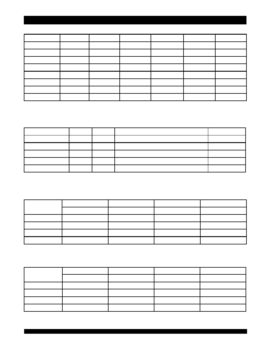
6.42
IDT71V433
32K x 32, 3.3V Synchronous SRAM with Flow-Through Outputs Commercial and Industrial Temperature Ranges
7
Linear Burst Sequence Table (LBO=V
SS
)
Interleaved Burst Sequence Table (LBO=V
DD
)
Asynchronous Truth Table
(1)
Synchronous Write Function Truth Table
(1)
NOTES:
1. L = V
IL
, H = V
IH
, X = Don't Care.
2. Multiple bytes may be selected during the same cycle.
Operation
GW
BWE
BW
1
BW
2
BW
3
BW
4
Read
H
H
X
X
X
X
Read
H
L
H
H
H
H
Write all Bytes
L
X
X
X
X
X
Write all Bytes
H
L
L
L
L
L
Write Byte 1
(2)
H
L
L
H
H
H
Write Byte 2
(2)
H
L
H
L
H
H
Write Byte 3
(2)
H
L
H
H
L
H
Write Byte 4
(2)
H
L
H
H
H
L
3729 tbl 08
NOTES:
1. L = V
IL
, H = V
IH
, X = Don't Care.
2. Synchronous function pins must be biased appropriately to satisfy operation requirements.
Operation
OE
ZZ
I/O Status
Power
Read
L
L
Data Out (I/O
0
≠I/O
31
)
Active
Read
H
L
High-Z
Active
Write
X
L
High-Z -- Data In (I/O
0
≠I/O
31
)
Active
Deselected
X
L
High-Z
Standby
Sleep Mode
X
H
High-Z
Sleep
3729 tbl 09
NOTE:
1. Upon completion of the Burst sequence the counter wraps around to its initial state.
Sequence 1
Sequence 2
Sequence 3
Sequence 4
A1
A0
A1
A0
A1
A0
A1
A0
First Address
0
0
0
1
1
0
1
1
Second Address
0
1
0
0
1
1
1
0
Third Address
1
0
1
1
0
0
0
1
Fourth Address
(1)
1
1
1
0
0
1
0
0
3729 tbl 10
NOTE:
1. Upon completion of the Burst sequence the counter wraps around to its initial state.
Sequence 1
Sequence 2
Sequence 3
Sequence 4
A1
A0
A1
A0
A1
A0
A1
A0
First Address
0
0
0
1
1
0
1
1
Second Address
0
1
1
0
1
1
0
0
Third Address
1
0
1
1
0
0
0
1
Fourth Address
(1)
1
1
0
0
0
1
1
0
3729 tbl 11
8
IDT71V433
32K x 32, 3.3V Synchronous SRAM with Flow-Through Outputs Commercial and Industrial Temperature Ranges
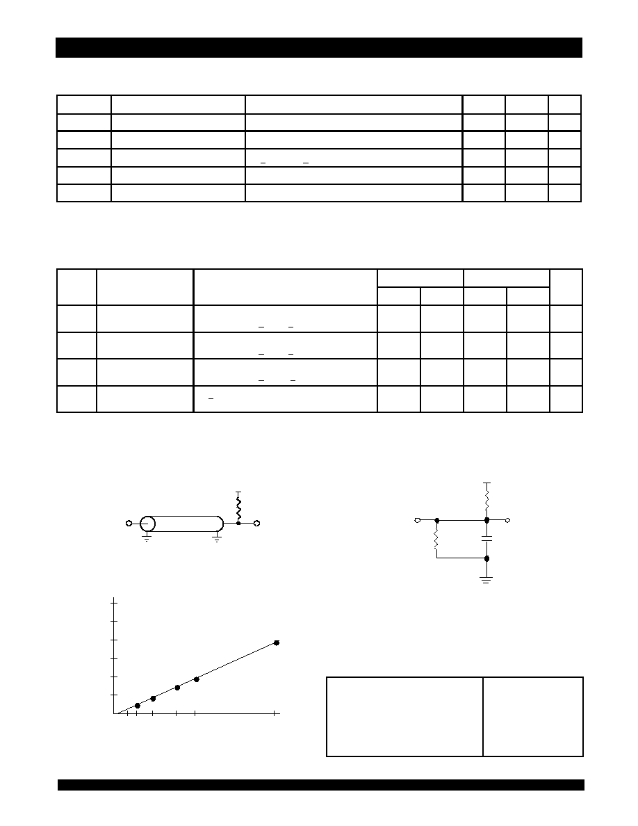
DC Electrical Characteristics Over the Operating Temperature and
Supply Voltage Range
(V
DD
= 3.3V +10/-5%, Commercial and Industrial Temperature Ranges)
Figure 3. Lumped Capacitive Load, Typical Derating
Figure 2. High-Impedence Test Load
(for t
OHZ
, t
CHZ
, t
OLZ
, and t
DC1)
DC Electrical Characteristics Over the Operating Temperature and
Supply Voltage Range
(1)
(V
HD
= V
DDQ
0.2V
,
V
LD
= 0.2V)
351
+3.3V
317
5pF*
3729 drw 04
DATA OUT
1
2
3
4
20 30 50
100
200
t
CD
(Typical, ns)
Capacitance (pF)
80
5
6
3729 drw 05
NOTE:
1. The
LBO pin will be internally pulled to V
DD
if it is not actively driven in the application and the ZZ pin will be internally pulled to V
SS
if not actively driven.
Symbol
Parameter
Test Conditions
Min.
Max.
Unit
|I
LI
|
Input Leakage Current
V
DD
= Max., V
IN
=
0V to V
DD
___
5
µ A
|I
LI
|
ZZ &
LBO Input Leakage Current
(1)
V
DD
= Max., V
IN
=
0V to V
DD
___
30
µ A
|I
LO
|
Output Leakage Current
CE > V
IH
or
OE > V
IH
, V
OUT
= 0V to V
DD
, V
DD
= Max.
___
5
µ A
V
OL
Output Low Voltage
I
OL
= 5mA, V
DD
= Min.
___
0.4
V
V
OH
Output High Voltage
I
OH
= ≠5mA, V
DD
= Min.
2.4
___
V
3729 tbl 12
NOTES:
1. All values are maximum guaranteed values.
2. At f = f
MAX,
inputs are cycling at the maximum frequency of read cycles of 1/t
CYC
while
ADSC = LOW; f=0 means no input lines are changing.
IDT71V433S11
IDT71V433S12
Symbol
Parameter
Test Conditions
Com'l.
Ind.
Com'l.
Ind.
Unit
I
DD
Operating Core Power
Supply Current
Device Selected, Outputs Open, V
DD
= Max.,
V
DDQ
= Max., V
IN
> V
IH
or < V
IL
, f = f
MAX
(2)
220
220
210
210
mA
I
SB
Standby Core Power
Supply Current
Device Deselected, Outputs Open, V
DD
= Max.,
V
DDQ
= Max., V
IN
> V
IH
or < V
IL
, f = f
MAX
(2)
45
45
40
40
mA
I
SB1
Full Standby Core Power
Supply Current
Device Deselected, Outputs Open, V
DD
= Max.,
V
DDQ
= Max., V
IN
> V
HD
or < V
LD
, f = 0
(2)
15
15
15
15
mA
I
ZZ
Full Sleep Mode Core
Power Supply Current
ZZ > V
HD
, V
DD
= Max.
15
15
15
15
mA
3729 tbl 13
* Including scope and jig capacitance.
AC Test Conditions
AC Test Loads
Figure 1. AC Test Load
50
DATA
OUT
Z
0
= 50
3729 drw 03
V
DDQ
/2
Input Pulse Levels
Input Rise/Fall Times
Input Timing Reference Levels
Output Timing Reference Levels
AC Test Load
0 to 3.0V
2ns
1.5V
1.5V
See Figures 1 and 2
3729 tbl 14
6.42
IDT71V433
32K x 32, 3.3V Synchronous SRAM with Flow-Through Outputs Commercial and Industrial Temperature Ranges
9
Symbol
Parameter
71V433S11
71V433S12
Unit
Min.
Max.
Min.
Max.
Clock Parameters
t
CYC
Clock Cycle Time
20
____
20
____
ns
t
CH
(1)
Clock High Pulse Width
6
____
6
____
ns
t
CL
(1)
Clock Low Pulse Width
6
____
6
____
ns
Output Parameters
t
CD
Clock High to Valid Data
____
11
____
12
ns
t
CDC
Clock High to Data Change
3
____
3
____
ns
t
CLZ
(2)
Clock High to Output Active
0
____
0
____
ns
t
CHZ
(2)
Clock High to Data High-Z
3
6
3
6
ns
t
OE
Output Enable Access Time
____
4
____
4
ns
t
OLZ
(2)
Output Enable Low to Data Active
0
____
0
____
ns
t
OHZ
(2)
Output Enable High to Data High-Z
____
6
____
6
ns
Setup Times
t
SA
Address Setup Time
2.5
____
2.5
____
ns
t
SS
Address Status Setup Time
2.5
____
2.5
____
ns
t
SD
Data in Setup Time
2.5
____
2.5
____
ns
t
SW
Write Setup Time
2.5
____
2.5
____
ns
t
SAV
Address Advance Setup Time
2.5
____
2.5
____
ns
t
SC
Chip Enable/Select Setup Time
2.5
____
2.5
____
ns
Hold Times
t
HA
Address Hold Time
0.5
____
0.5
____
ns
t
HS
Address Status Hold Time
0.5
____
0.5
____
ns
t
HD
Data In Hold Time
0.5
____
0.5
____
ns
t
HW
Write Hold Time
0.5
____
0.5
____
ns
t
HAV
Address Advance Hold Time
0.5
____
0.5
____
ns
t
HC
Chip Enable/Select Hold Time
0.5
____
0.5
____
ns
Sleep Mode and Configuration Parameters
t
ZZPW
ZZ Pulse Width
100
____
100
____
ns
t
ZZR
(3)
ZZ Recovery Time
100
____
100
____
ns
t
CFG
(4)
Configuration Set-up Time
80
____
80
____
ns
3729 tbl 15
AC Electrical Characteristics
(V
DD
= 3.3V +10/-5%, Commercial and Industrial Temperature Ranges)
NOTES:
1. Measured as HIGH above 2.0V and LOW below 0.8V.
2. Transition is measured ±200mV from steady-state.
3. Device must be deselected when powered-up from sleep mode.
4. t
CFG
is the minimum time required to configure the device based on the
LBO input. LBO is a static input and must not change during normal operation.
10
IDT71V433
32K x 32, 3.3V Synchronous SRAM with Flow-Through Outputs Commercial and Industrial Temperature Ranges
NOTES:
1
.
O1 (Ax) represents the first output from the external address Ax. O1 (Ay) represents the first output from the external addre
ss Ay; O2 (Ay) represents the next output data in the burst sequence of the base
address Ay, etc., where A
0
and A
1
are advancing for the four word burst in the sequence defined by the state of the
LBO
input.
2
.
ZZ input is LOW and
LBO
is Don't Care for this cycle.
3.
C
S
0
timing transitions are identical but inverted to the
CE
and
CS
1
signals. For example, when
CE
and
CS
1
are LOW on this waveform, CS
0
is HIGH.
Timing Waveform of Read Cycle
(1,2)
t
C
H
Z
t
S
A
t
S
C
t
H
S
G
W
,
B
W
E
,
B
W
x
t
S
W
t
C
L
t
S
A
V
t
H
W
t
H
A
V
C
LK
A
D
S
P
A
D
S
C
(1
)
A
D
D
R
E
S
S
t
C
Y
C
t
C
H
t
H
A
t
H
C
t
O
E
t
O
H
Z
O
E
t
C
D
t
O
L
Z
O
1(
A
x)
D
A
T
A
O
U
T
t
C
D
C
O
1(
A
y)
O
2
(A
y)
O
2(
A
y)
A
D
V
A
D
V
in
s
e
r
t
s
a
w
ai
t
-
s
t
at
e
C
E
,
C
S
1
(N
ot
e
3
)
372
9
dr
w
06
F
lo
w
-
t
hr
ou
g
h
R
ea
d
B
ur
st
F
lo
w
-
t
h
r
ou
gh
R
ea
d
O
ut
pu
t
D
is
a
b
l
e
d
A
x
A
y
t
S
S
O
1(
A
y)
O
4(
A
y)
O
3(
A
y)
(B
ur
s
t
w
raps
arou
nd
to
it
s
in
it
ia
l
s
t
a
t
e
)
.
6.42
IDT71V433
32K x 32, 3.3V Synchronous SRAM with Flow-Through Outputs Commercial and Industrial Temperature Ranges
11
Timing Waveform of Combined Read and Write Cycles
(1,2,3)
NOTES:
1
.
Device is selected through entire cycle;
CE
and
CS
1
are LOW, CS
0
is HIGH.
2
.
ZZ input is LOW and
LBO
is Don't Care for this cycle.
3
.
O1 (Ax) represents the first output from the external address Ax. I1 (Ay) represents the first input from the external addres
s Ay. O1 (Az) represents the first output from the external address Az; O2 (Az) represents
the next output data in the burst sequence of the base address Az, etc., where A
0
and A
1
are advancing for the four word burst in the sequence defined by the state of the
LBO
input.
O
1(A
z)
C
LK
A
D
S
P
A
D
D
R
E
S
S
G
W
A
D
V
O
E
D
A
T
A
O
U
T
t
C
Y
C
t
C
H
t
C
L
t
H
A
t
S
W
t
H
W
t
C
LZ
A
x
A
y
A
z
I1
(
A
y)
t
S
D
t
H
D
t
O
LZ
t
C
D
t
C
D
C
D
A
T
A
IN
(2
)
t
O
E
O
1(A
z)
3
729
dr
w
07
S
i
ngl
e
R
ead
F
lo
w
-t
hrough
B
urs
t
R
ead
W
ri
t
e
t
O
H
Z
t
S
S
t
S
A
O
3(A
z)
O
2(A
z)
O
4(A
z)
O
1(A
x)
.
t
H
S
12
IDT71V433
32K x 32, 3.3V Synchronous SRAM with Flow-Through Outputs Commercial and Industrial Temperature Ranges
Timing Waveform of Write Cycle No. 1 GW Controlled
(1,2,3)
NOTES:
1
.
ZZ input is LOW,
BWE
is HIGH, and
LBO
is Don't Care for this cycle.
2
.
O4 (Aw) represents the final output data in the burst sequence of the base address Aw. I1 (Ax) represents the first input fro
m the external address Ax. I1 (Ay) represents the first input from the external address
Ay; I2 (Ay) represents the next input data in the burst sequence of the base address Ay, etc., where A
0
and A
1
are advancing for the four word burst in the sequence defined by the state of the
LBO
input. In
the case of input I2(Ay) this data is valid for two cycles because
ADV
is high and has suspended the burst.
3.
C
S
0
timing transitions are identical but inverted to the
CE
and
CS
1
signals. For example, when
CE
and
CS
1
are LOW on this waveform, CS
0
is HIGH.
37
29
dr
w
08
A
D
D
R
E
S
S
C
LK
A
D
S
P
A
D
S
C
t
C
Y
C
t
S
S
t
H
S
t
C
H
t
C
L
t
H
A
t
S
A
A
x
A
y
A
z
A
D
V
D
A
TA
O
U
T
O
E
t
H
C
t
S
D
I1
(
A
x)
I1
(
A
z)
I2
(
A
y)
tH
D
t
O
H
Z
D
A
TA
IN
t
H
A
V
O
4(
A
w
)
C
E
,
C
S
1
G
W
t
S
W
(N
ot
e
3)
I2
(A
z)
I3
(A
z)
I4
(A
y)
I3
(
A
y)
I2
(A
y)
t
S
A
V
(
A
D
V
s
u
s
pen
ds
bu
rs
t
)
I1
(
A
y)
B
W
E
is
ign
or
ed
w
he
n
A
D
S
P
in
it
iat
es
bu
rs
t
t
S
C
(1
)
(3
)
O
3(
A
w
)
.
t
H
W
6.42
IDT71V433
32K x 32, 3.3V Synchronous SRAM with Flow-Through Outputs Commercial and Industrial Temperature Ranges
13
Timing Waveform of Write Cycle No. 2 Byte Controlled
(1,2,3)
NOTES:
1
.
ZZ input is LOW,
GW
is HIGH, and
LBO
is Don't Care for this cycle.
2
.
O4 (Aw) represents the final output data in the burst sequence of the base address Aw. I1 (Ax) represents the first input fro
m the external address Ax. I1 (Ay) represents the first input from the external address
Ay; I2 (Ay) represents the next input data in the burst sequence of the base address Ay, etc., where A
0
and A
1
are advancing for the four word burst in the sequence defined by the state of the
LBO
input.
In the case of input I2(Ay) this data is valid for two cycles because
ADV
is high and has suspended the burst.
3.
C
S
0
timing transitions are identical but inverted to the
CE
and
CS
1
signals. For example, when
CE
and
CS
1
are LOW on this waveform, CS
0
is HIGH.
A
D
D
R
E
S
S
C
LK
A
D
S
P
A
D
S
C
t
C
Y
C
t
S
S
t
H
S
t
C
H
t
C
L
t
H
A
t
S
A
A
x
A
y
B
W
x
A
D
V
D
A
T
A
O
U
T
O
E
t
H
C
t
S
D
S
i
ngl
e
W
ri
t
e
B
ur
s
t
W
ri
te
I1
(
A
x)
I2
(
A
y)
I2
(A
y)
(
A
D
V
su
s
pend
s
b
ur
s
t
)
I2
(
A
z)
tH
D
R
ea
d
B
ur
s
t
E
xt
en
de
d
B
ur
st
W
ri
te
t
O
H
Z
D
A
T
A
IN
t
S
A
V
t
S
W
O
4(
A
w
)
C
E
,
C
S
1
B
W
E
t
S
W
(N
o
te
3)
I1
(A
z)
A
z
I4
(A
y)
I1
(A
y)
37
29
dr
w
09
I4
(A
y)
I3
(A
y)
t
S
C
B
W
E
is
ig
nor
e
d
w
hen
A
D
S
P
in
it
ia
te
s
bur
s
t
B
W
x
is
i
gno
re
d
w
h
en
A
D
S
P
in
it
ia
t
e
s
bu
rs
t
I3
(A
z)
O
3(
A
w
)
.
t
H
W
t
H
W
14
IDT71V433
32K x 32, 3.3V Synchronous SRAM with Flow-Through Outputs Commercial and Industrial Temperature Ranges
Timing Waveform of Sleep (ZZ) and Power-Down Modes
(1,2,3)
NOTES:
1
.
Device must power up in deselected mode.
2.
LBO
input is Don't Care for this cycle.
3
.
It is not necessary to retain the state of the input registers throughout the Power-down cycle.
4.
C
S
0
timing transitions are identical but inverted to the
CE
and
CS
1
signals. For example, when
CE
and
CS
1
are LOW on this waveform, CS
0
is HIGH.
t
C
Y
C
t
S
S
t
C
L
t
C
H
t
H
A
t
S
A
t
S
C
t
H
C
t
O
E
t
O
LZ
t
H
S
C
LK
A
D
S
P
A
D
S
C
A
D
D
R
E
S
S
G
W
C
E
,
C
S
1
A
D
V
D
A
T
A
O
U
T
O
E
Z
Z
S
in
g
l
e
R
ea
d
S
noo
ze
M
od
e
t
Z
Z
P
W
37
29
d
rw
10
O
1(
A
x)
A
x
(N
ot
e
4)
t
Z
Z
R
A
z
.
6.42
IDT71V433
32K x 32, 3.3V Synchronous SRAM with Flow-Through Outputs Commercial and Industrial Temperature Ranges
15
Non-Burst Read Cycle Timing Waveform
NOTES:
1
ZZ input is LOW,
ADV is HIGH, and LBO is Don't Care for this cycle.
2. (Ax) represents the data for address Ax, etc.
3. For read cycles,
ADSP and ADSC
function identically and are therefore interchangeable.
CLK
ADSP
GW
,
BWE
,
BW
x
CE
,
CS
1
CS
0
ADDRESS
ADSC
DATA
OUT
OE
Av
Aw
Ax
Ay
Az
3729 drw 11
(Av)
(Aw)
(Ax)
(Ay)
.
16
IDT71V433
32K x 32, 3.3V Synchronous SRAM with Flow-Through Outputs Commercial and Industrial Temperature Ranges
Non-Burst Write Cycle Timing Waveform
NOTES:
1. ZZ input is LOW,
ADV and OE are HIGH, and LBO is Don't Care for this cycle.
2. (Ax) represents the data for address Ax, etc.
3. Although only
GW writes are shown, the functionality of BWE and BWx together is the same as GW.
4. For write cycles,
ADSP and ADSC
have different limitations.
CLK
ADSP
GW
CE
,
CS
1
CS
0
ADDRESS
ADSC
DATA
IN
Av
Aw
Ax
Az
Ay
(Av)
(Aw)
(Ax)
(Az)
(Ay)
3729 drw 12
.
6.42
IDT71V433
32K x 32, 3.3V Synchronous SRAM with Flow-Through Outputs Commercial and Industrial Temperature Ranges
17
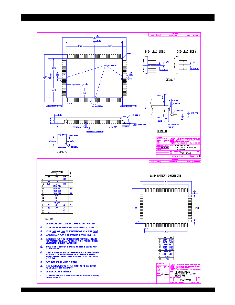
100-Pin Thin Quad Flatpack (TQFP) Package Diagram Outline
18
IDT71V433
32K x 32, 3.3V Synchronous SRAM with Flow-Through Outputs Commercial and Industrial Temperature Ranges
Ordering Information
Plastic Thin Quad Flatpack, 100 pin (PK100-1)
S
Power
X
Speed
PF
Package
PF
IDT
71V433
11
12
t
CD
in nanoseconds
3729 drw 13
Device
Type
PART NUMBER
SPEED IN MEGAHERTZ
t
CD
PARAMETER
CLOCK CYCLE TIME
50 MHz
50 MHz
11 ns
12 ns
20 ns
20 ns
.
X
Process/
Temperature
Range
Blank
I
Commercial (0
∞
C to +70
∞
C)
Industrial (≠40
∞
C to +85
∞
C)
71V433S11PF
71V433S12PF

6.42
IDT71V433
32K x 32, 3.3V Synchronous SRAM with Flow-Through Outputs Commercial and Industrial Temperature Ranges
19
CORPORATE HEADQUARTERS
for SALES:
for TECH SUPPORT:
2975 Stender Way
800 345-7015 or 408 727-6116
sramhelp@idt.com
Santa Clara, CA 95054
fax: 408 492-8674
800 544-7726, x4033
www.idt.com
The IDT logo is a registered trademark of Integrated Device Technology, Inc.
Datasheet Document History
09/10/99
Updated to new format
Pg. 1, 8, 9, 17
Revised speed offerings to 11 and 12 ns at 50 MHz
Pg. 3≠5
Adjusted page layout, added extra page
Pg. 5
Added notes to pin configuration
`
Pg. 11≠14
Updated notes
Pg. 18
Added Datasheet Document History
10/08/99
Pg. 1, 4, 8, 9, 17
Added Industrial temperature range offerings
04/04/00
Pg. 17
Added 100pinTQFP Package Diagram Outline
08/09/00
Not recommended for new designs
08/17/01
Removed "Not recommended for new designs" from the background on the datasheet